IEEE Transactions on VLSI 2024
Following Novelty based Research Projects not yet Published in Any Journal
Customization Available for Journal Publications
A High Speed CRC-32 Implementation on FPGA
Base Paper Abstract:
Cyclic Redundancy Check (CRC) is widely used for transmission error detection in various communication interfaces. As the transmission rate increases, accelerating CRC with lower resource consumption for high-speed interfaces becomes significant. This paper analyzes and implements a typical CRC algorithm (Stride-x) and designs a padding-zero strategy to support the input data length with multiples of byte. Besides, experiments are conducted to validate the proposed algorithm on Xilinx FPGA platforms. When stride is 1, the proposed algorithm outperforms a typical parallel CRC algorithm in throughput and resource consumption with various input bus widths (32/128/256 bits).
List of the following materials will be included with the Downloaded Backup: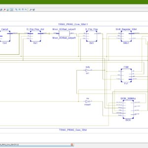
A Hybrid TRNG-PRNG Architecture for High-Performance and Resource-Efficient Random Number Generation on FPGA
Base Paper Abstract:
True random number generators (TRNGs) are fundamentals in many important security applications. Though they exploit randomness sources that are typical of the analog domain, digital-based solutions are strongly required especially when they have to be implemented on Field Programmable Gate Array (FPGA)-based digital systems. This paper describes a novel methodology to easily design a TRNG on FPGA devices. It exploits the runtime capability of the Digital Clock Manager (DCM) hardware primitives to tune the phase shift between two clock signals. The presented auto-tuning strategy automatically sets the phase difference of two clock signals in order to force on one or more flip-flops (FFs) to enter the metastability region, used as a randomness source. Moreover, a novel use of the fast carry-chain hardware primitive is proposed to further increase the randomness of the generated bits. Finally, an effective on-chip post-processing scheme that does not reduce the TRNG throughput is described. The proposed TRNG architecture has been implemented on the Xilinx Zynq XC7Z020 System on Chip (SoC). It passed all the National Institute of Standards and Technology (NIST) SP 800-22 statistical tests with a maximum throughput of 300×106 bit per second. The latter is considerably higher than the throughput of other previously published DCM based TRNGs.
List of the following materials will be included with the Downloaded Backup: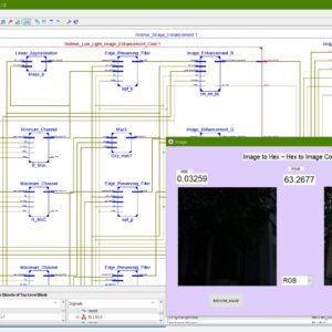
A Low Cost FPGA Implementation of Retinex Based Low-Light Image Enhancement Algorithm
Base Paper Abstract:
Real-time low-light image enhancement has several potential applications, such as advanced driver assistance systems (ADAS), remote sensing, object tracking, etc. The Retinex-based algorithms are mostly used to restore the visibility of low-light images. However, they perform complex mathematical operations over a large spatial window. Consequently, their hardware realization is tedious, and few researchers have attempted to address this problem. In this brief, we propose a Retinex-based algorithm that employs a low-cost edge-preserving filter for illumination estimation. Although certain approximations are used to curtail the hardware logic resource requirement, the quality of the enhanced image is not compromised. The proposed architecture requires only 10868 LUTs and 7409 registers when implemented on ZynQ 7 FPGA. Moreover, it can process HD images (1920×1080) at the rate of 60 frames per second (fps).
List of the following materials will be included with the Downloaded Backup: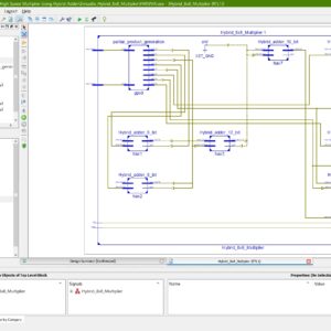
A Novel Design of High Speed Multiplier Using Hybrid Adder Technique
Base Paper Abstract:
Electronic devices are necessary in small spaces in order to provide fast speed and low power consumption. Arithmetic operations determine how quickly electronics operate. In many applications involving VLSI signal processing, multiplication is a necessary arithmetic operation. Thus, to create any kind of signal processing module, a high-speed multiplier is a prerequisite. Every individual has different needs and goals, which has led to the development of different multipliers according to the need of application. In this paper, a Hybrid multiplier is proposed and designed using hybrid adders which is a mixture of Brent Kung adder and Kogge Stone adder which results in less delay i.e. 4.062ns compared to other multipliers existed.
List of the following materials will be included with the Downloaded Backup:
An Aadhaar-Authenticated FPGA-Based Electronic Voting Machine with EPIC Key Derived
Base paper Abstract:
Electronic voting machines are widely used to improve election transparency, reduce manual effort, and provide faster result declaration when compared to traditional paper-based voting systems. The integration of digital platforms further enables ease of access, efficient data handling, and automated vote counting. However, existing electronic voting solutions still face critical challenges such as voter impersonation, data tampering, weak software-based security, and lack of strong hardware-level protection, especially when sensitive voter identity information is involved. Most current systems rely on microcontroller-based architectures, centralized databases, or conventional cryptographic algorithms, which introduce vulnerabilities related to key management, higher computational cost, and limited resistance to physical and logical attacks. To address these issues, this work proposes an Aadhaar-authenticated FPGA-based electronic voting machine with EPIC key–derived lightweight cryptographic vote protection. In the proposed system, Aadhaar number and Voter ID (EPIC) information are captured through a MATLAB-based graphical user interface and securely stored as voter records. The EPIC number is used to derive an 80-bit cryptographic key, while the complete voter information is formatted into a 256-bit data frame and processed within FPGA block memory. Lightweight PRESENT cipher encryption, along with cipher and key shuffling techniques, is employed to protect voter data at the hardware level, ensuring confidentiality and integrity. Decryption is performed using a reverse process to enable authenticated vote verification and result checking without exposing encrypted data. The novelty of this work lies in EPIC key–based dynamic key generation combined with FPGA-based lightweight cryptography, eliminating external key storage and reducing attack surfaces. The system ensures secure authentication, tamper resistance, low resource utilization, and reliable vote verification. Performance and functionality are validated using MATLAB for GUI and data handling, and Verilog HDL for FPGA implementation, demonstrating a secure, efficient, and hardware-trusted electronic voting solution.
List of the following materials will be included with the Downloaded Backup: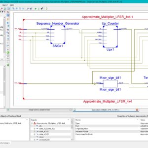
Approximate Multiplier Design with LFSR-Based Stochastic Sequence Generators for Edge AI
Base Paper Abstract:
This letter introduces an innovative approximate multiplier (AM) architecture that leverages stochastically generated bit streams through the Linear Feedback Shift Register (LFSR). The AM is applied to matrix-vector multiplication (MVM) in Neural Networks (NNs). The hardware implementations in 90 nm CMOS technology demonstrate superior power and area efficiency compared to state-of-the-art designs. Additionally, the study explores applying stochastic computing to LSTM NNs, showcasing improved energy efficiency and speed.
List of the following materials will be included with the Downloaded Backup:
Design and Implementation of 32-bit CSPRNG using the PRESENT cipher with Dual Polynomial PRNG for Enhanced Randomness and Precision
Base Paper Abstract:
Random Number Generators (RNGs) are substantially used in many security domains, providing a fundamental source of unpredictability essential for tasks such as cryptography, simulations, and statistical analyses. The efficiency and quality of an RNG directly impact the reliability and security of diverse applications, making advancements in RNG design, as explored in this study, of significant importance for enhancing computational processes. This paper presents an innovative Pseudo-Random Number Generator (PRNG) that leverages the efficiency of two carefully selected Linear Feedback Shift Registers (LFSRs) and a connecting XOR gate. The investigation of five polynomials identified an optimal pair, resulting in a notable improvement of over 200X in the length of random bit sequences compared to a single LFSR-based PRNG. The Basys3 FPGA board with the xc7a35tcpg236-1 FPGA chip was used to implement and synthesize the proposed design. Two significant findings emerge from this research. Firstly, using variable polynomials demonstrates a huge enhancement in the duration of randomness, outperforming the impact of variable seeds. A noteworthy observation is that employing the same polynomials in different branches does not result in optimal results. Secondly, managing more seeds is associated with an increased area cost, underscoring the efficiency of handling two polynomials.
List of the following materials will be included with the Downloaded Backup: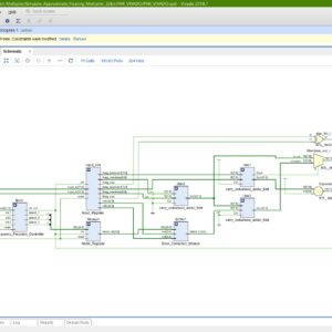
Efficient Approximate Floating-Point Multiplier with Runtime Reconfigurable Frequency and Precision
Base Paper Abstract:
Deep Neural Networks (DNNs) perform intensive matrix multiplications but can tolerate inaccurate intermediate results to some degree. This makes them a perfect target for energy reduction by approximate computing. However, current research in this direction requires DNNs redesign and does not provide the flexibility for users to trade accuracy for energy saving. In this brief, we propose a runtime reconfigurable approximate floating-point multiplier and present details of its hardware implementation. The flexible computation precision is provided by our error correction module, which is controlled by reconfigurable clock signals. The circuit design solves the glitch and metastability problems. The proposed approximate multiplier with three precision levels is evaluated on Synopsys design compiler and Xilinx FPGA platforms. Experimental results demonstrate the advantages of our approach in terms of speed, hardware overhead, and power consumption, while ensuring a controllable accuracy loss for DNNs inferences.
List of the following materials will be included with the Downloaded Backup: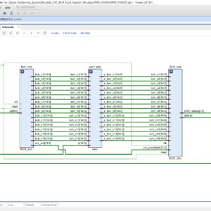
Efficient CRC-BCH Unified Encoder for Global Positioning System
Base Paper Abstract:
GPS uses ECCs to see if an error occurs when the data sent from the satellite reaches the user. Each message structure uses ECCs such as Hamming Code, CRC, BCH Code, and LDPC Code. If the satellite contains all of the encoders, it has a negative impact to the area and power consumption. Therefore, in this paper, we propose a CRC-BCH unified encoder for GPS, which is efficient in terms of space and power consumption. Since both the CRC and BCH encoders use shift registers, the design was made using this part. To replace the existing encoder, the CRC-BCH encoder must have the same output. To validate this, we used individual CRC and BCH encoders and confirmed that the generated output was identical to the output of the proposed encoder. The proposed CRC-BCH unified encoder was synthesized at an operating frequency of 400 MHz using the CMOS 28nm process. The synthesis results showed that it used 16.67% less area and consumed 19.68% less power than the existing encoder. Therefore, the proposed CRC-BCH unified encoder offers advantages in terms of satellite weight and energy efficiency.
List of the following materials will be included with the Downloaded Backup: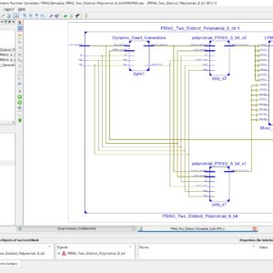
Efficient Pseudo Random Number Generator (PRNG) Design on FPGA
Proposed Abstract:
Random Number Generators (RNGs) are substantially used in many security domains, providing a fundamental source of unpredictability essential for tasks such as cryptography, simulations, and statistical analyses. The efficiency and quality of an RNG directly impact the reliability and security of diverse applications, making advancements in RNG design, as explored in this study, of significant importance for enhancing computational processes. This paper presents an innovative Pseudo-Random Number Generator (PRNG) that leverages the efficiency of two carefully selected Linear Feedback Shift Registers (LFSRs) and a connecting XOR gate. The investigation of five polynomials identified an optimal pair, resulting in a notable improvement of over 200X in the length of random bit sequences compared to a single LFSR-based PRNG. The Basys3 FPGA board with the xc7a35tcpg236-1 FPGA chip was used to implement and synthesize the proposed design. Two significant findings emerge from this research. Firstly, using variable polynomials demonstrates a huge enhancement in the duration of randomness, outperforming the impact of variable seeds. A noteworthy observation is that employing the same polynomials in different branches does not result in optimal results. Secondly, managing more seeds is associated with an increased area cost, underscoring the efficiency of handling two polynomials.
List of the following materials will be included with the Downloaded Backup:
Energy Efficient Compact Approximate Multiplier for Error-Resilient Applications
Base Paper Abstract:
The primary goal of approximate computing is enhancing system performance, such as energy efficiency, speed, and form factor. Despite the growing use of approximate multipliers, the design of efficient approximate compressors — a fundamental multiplier block — remains a significant challenge. In this brief, 8-transistor and 14-transistor 4:2 compressors are proposed. Both compressors exploit CMOS technology and a constant and conditional approximation of selected inputs, exhibiting fewer negative errors. As a result, a resource-expensive error recovery module is eliminated, yielding superior performance as compared with prior art. The 14-transistor architecture yields a lower error rate compared to the 8-transistor architecture, trading off lower area for higher accuracy. The compressor tailored circuit architecture is also proposed and evaluated using image multiplication. The proposed multiplier exhibits 50% area savings and 93% lower power-delay-product compared to the exact multiplier, as well as higher accuracy, and 38% PDP enhancement compared with the state-of-the-art.
List of the following materials will be included with the Downloaded Backup: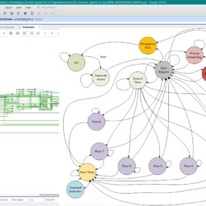
FPGA Implementation of Intelligent Elevator System for AI Applications
Proposed Abstract:
Intelligent elevator systems are used in many smart buildings, offices, hospitals, and tall apartments to move people quickly, reduce waiting time, and save energy. They have many advantages, like faster operation, better safety, and the ability to handle requests from many floors at the same time. But there are also some disadvantages, such as slow response when many people use them, fixed movement patterns that cannot adjust to real-time needs, weak security for restricted floors, and no use of advanced AI features for learning and prediction. Most existing elevator systems are built using microcontrollers with fixed scheduling methods, which cannot easily change their operation or add smart features. The problem in this work is to create an elevator system that works faster, is more secure, can adjust to different situations, and is ready for AI use, while also keeping passengers safe. In this project, we design an elevator controller on FPGA using a finite state machine. The system includes floor request handling, priority scheduling, emergency stop, overload detection, automatic door timing, floor number display, passcode access for special floors, and a fire alarm mode. The new idea in this work is to use the speed and flexibility of FPGA hardware along with an FSM design that can later connect to AI for learning passenger habits and predicting movement needs. This makes the system quick, safe, and adaptable. The design is written in Verilog HDL, tested in ModelSim, and implemented on a Xilinx FPGA board. We measure performance by checking response time, scheduling efficiency, and safety accuracy, and the results show it is suitable for future smart building use.
List of the following materials will be included with the Downloaded Backup:
FPGA IP Core for DC Motor Control with Adaptive Neural Network PID Tuning
Base paper Abstract:
Traditional proportional integral derivative (PID) falls short for precise control of DC motor speed under changing conditions. This paper presents a novel FPGA based IP (intellectual property) core for real-time PID parameter adjustment utilizing a multilayer neural network and the back propagation neural network algorithm. The design is implemented entirely in verilog HDL (hardware description language) using the Vivado 2023.1 tool in the Zynq 7z020 SoC (system on chip), with highly efficient resource utilization of 7.37% look-up table (LUT), 1.92% flip-flops, and 3.57% memory. The co-simulation results show a fast rise time of 0.00496s, a settling time of 0.0083s, a lower integral absolute error (IAE) of 0.045, and a minimum overshoot of 0.45%, validating the effectiveness of the proposed controller for comprehensive motion control systems. This dynamic approach outperforms traditional PID controllers by adapting to changing conditions, significantly improving rise time and settling time, which are critical factors in healthcare applications. Other key features of this work include precise duty cycle generation at a 10 kHz switching frequency for accurate motor speed control and an incremental encoder interface for high-resolution position feedback.
List of the following materials will be included with the Downloaded Backup: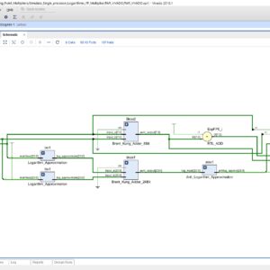
Hardware-Efficient Logarithmic Floating-Point Multipliers for Error-Tolerant Applications
Base Paper Abstract:
The increasing computational intensity of important new applications poses a challenge for their use in resource restricted devices. Approximate computing using power-efficient arithmetic circuits is one of the emerging strategies to reach this objective. In this article, five hardware-efficient logarithmic floating-point (FP) multipliers are proposed, which all use simple operators, such as adders and multiplexers, to replace complex and costlier conventional FP multipliers. Radix-4 logarithms are used to further reduce the hardware complexity. These designs produce double-sided error distributions to mitigate error accumulation in complex computations. The proposed multipliers provide superior trade-offs between accuracy and hardware, with up to 30.8% higher accuracy than a recent logarithmic FP design or up to 68× less energy than the conventional FP multiplier. Using the proposed FP logarithmic multipliers in JPEG image compression achieves higher image quality than a recent logarithmic multiplier design with up to 4.7 dB larger peak signal-to-noise ratio. For training in benchmark NN applications, the proposed FP multipliers can slightly improve the classification accuracy while achieving 4.2× less energy and 2.2× smaller area than the state-of-the-art design.
List of the following materials will be included with the Downloaded Backup: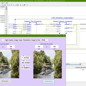
Hardware-Optimized High-Quality Super-Resolution Accelerator for Real-Time Edge Computing
Base Paper Abstract:
Super-resolution (SR) techniques have been employed to construct high-definition images from low-quality images. Various neural networks have demonstrated excellent image-reconstruction quality in SR accelerators. However, deploying SR networks on edge devices is limited by resources and power consumption induced by significant algorithm parameters, computation complexity, and external memory accesses. This work explores the hardware algorithm co-design techniques to provide an end-to-end platform with a lightweight super-resolution network (LSR) and an efficient, high-quality SR accelerator HDSuper. For algorithm design, the improved depth-wise separable convolution and pixel shuffle layers are developed to reduce network size and computation complexity by considering the hardware constraints. Also, the improved channel attention (CA) blocks enhance the image reconstruction quality. For hardware accelerator design, we design a unified computing core (UCC) combined with an efficient flattening-and allocation (F-A) mapping strategy to support various operators with high computational utilization. In addition, we design the patch computing scheme to reduce the external memory access of the hardware architecture. Based on the evaluation, the proposed algorithm achieves high-quality image reconstruction with 37.44d B PSNR. Finally, the FPGA demonstration and ASIC layout under UMC 55nm are achieved with low power consumption (2.08 W and 152mW) under the lowest hardware resources compared to the state-of-the-art works.
List of the following materials will be included with the Downloaded Backup: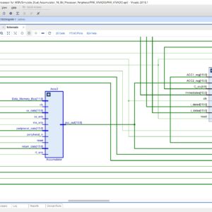
Optimized Dual Accumulator based RISC Architecture with Advanced Memory and Peripheral Operations
Proposed Abstract:
This paper presents an optimized Reduced Instruction Set Computer (RISC) architecture that leverages a dual accumulator design to enhance computational efficiency and performance. The architecture is scheduled to support advanced memory management and peripheral operations, addressing the growing need for high-speed data processing in embedded systems. The dual accumulator approach allows for parallel execution of arithmetic operations, reducing the number of instruction cycles and improving overall throughput. The architecture is designed with a focus on optimizing area, delay, and power consumption, making it suitable for resource-constrained environments. The proposed design is implemented using Verilog HDL and synthesized on the Xilinx Vivado platform targeting the Zynq FPGA. The architecture’s performance is verified through extensive simulation in Modelsim, and a comparative analysis is conducted to evaluate the improvements in key parameters such as area utilization, processing delay, and power efficiency. The results demonstrate that the optimized dual accumulator-based RISC architecture significantly outperforms traditional single accumulator designs, making it an ideal solution for modern embedded applications that require both high performance and low power consumption.
List of the following materials will be included with the Downloaded Backup: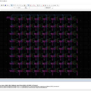
Soft-Error-Aware SRAM with Multinode Upset Tolerance for Aerospace Applications
Base Paper Abstract:
As technology scales down, the critical charge (QC) of vulnerable nodes decreases, making SRAM cells more susceptible to soft errors in the aerospace industry. This article proposes a Soft-Error-Aware 16T (S8P8N) SRAM cell for aerospace applications to address this issue. The properties of S8P8N are evaluated and compared with 6T, DICE, QUCCE12T, WEQUATRO, RHBD10T, RHBD12T, S4P8N, SEA14T, and SRRD12T. Simulation results indicate that all vulnerable nodes and key node pairs of the proposed cell can recover to their original states when affected by a soft error. Additionally, it can recover from key multinode upsets. The write speed of the proposed cell is found to be reduced by 20.3%, 50.1%, 74.1%, 63.7%, and 50.41% compared to 6T, DICE, QUCCE12T, WEQUATRO, and RHBD10T, respectively. The read speed of the proposed cell is found to be reduced by 56.6%, 52.2%, 62.5%, and 35.2% compared to 6T, SRRD12T, RHBD12T, and S4P8N, respectively. It also shows that the hold power of the proposed cell is found to be reduced by 14.1%, 13.8%, 17.7%, and 23.4% compared to DICE, WEQUATRO, RHBD10T, and RHBD12T. Furthermore, the read static noise margin (RSNM) of the proposed cell is found to be enhanced by 157%, 67%, and 32% compared to RHBD12T, SEA14T, and SRRD12T. All these improvements are achieved with a slight area penalty.
List of the following materials will be included with the Downloaded Backup:EEE Transactions on VLSI 2024, VLSI 2024 IEEE Project, VLSI Low Power 2024 Project, VLSI High Speed 2024 Project, VLSI Area Efficient 2024 Project, Low Cost VLSI 2024 Projects, High Speed VLSI Design 2024 projects ( CDMA, RTOS, DSP, RF, IF, etc), Low Power VLSI Design 2024 projects, Area Efficient VLSI Design 2024 projects , Audio processing VLSI Design 2024 projects, Signal Processing VLSI Design 2024 projects, Image Processing VLSI Design 2024 projects, Backend VLSI Design 2024 projects ( CMOS, TFET, BisFET, FeFET, etc), Timing & Delay Reduction VLSI 2024 Projects, Internet of Things VLSI 2024 Projects, Testing, Reliability and Fault Tolerance VLSI Projects, VLSI Applications ( Communicational, Video, Security, Sensor Networks, etc), SOC VLSI Projects, Network on Chip VLSI Projects, Wireless Communication VLSI Projects, VLSI Verifications Projects ( UVM, OVM, VVM, System Verilog).
Provide Wordlwide Online Support
We can provide Online Support Wordlwide, with proper execution, explanation and additionally provide explanation video file for execution and explanations.
24/7 Support Center
NXFEE, will Provide on 24x7 Online Support, You can call or text at +91 9789443203, or email us nxfee.innovation@gmail.com
Terms & Conditions:
Customer are advice to watch the project video file output, and before the payment to test the requirement, correction will be applicable.
After payment, if any correction in the Project is accepted, but requirement changes is applicable with updated charges based upon the requirement.
After payment the student having doubts, correction, software error, hardware errors, coding doubts are accepted.
Online support will not be given more than 3 times.
On first time explanation we can provide completely with video file support, other 2 we can provide doubt clarifications only.
If any Issue on Software license / System Error we can support and rectify that within end of day.
Extra Charges For duplicate bill copy. Bill must be paid in full, No part payment will be accepted.
After payment, to must send the payment receipt to our email id.
Powered by NXFEE INNOVATION, Pondicherry.
Call us today at : +91 9789443203 or Email us at nxfee.innovation@gmail.com
NXFEE Development & Services

Product Categories
- 2014 (11)
- 2015 (39)
- 2016 (30)
- 2017 (16)
- 2018 (17)
- 2019 (42)
- 2020 (29)
- 2021 (17)
- 2022 (23)
- Accessories (40)
- Area Efficient (115)
- High speed VLSI Design (56)
- IEEE (15)
- Image Processing (40)
- Low power VLSI Design (94)
- NOC VLSI Design (2)
- VLSI (245)
- VLSI 2023 (21)
- VLSI 2024 (17)
- VLSI 2025 (28)
- VLSI 2026 (2)
- VLSI Application / Interface and Mini Projects (31)
- VLSI_2023 (15)
Filter by price
Product Status
Sort by producents

Copyright © 2026 Nxfee Innovation.