No products in the cart.
Return To ShopHDFC BANK ACCOUNT:
- NXFEE INNOVATION,
HDFC BANK, MAIN BRANCH, PONDICHERRY-605004.
INDIA,
ACC NO. 50200090465140,
IFSC CODE: HDFC0000407.

₹10,000.00 Original price was: ₹10,000.00.₹6,000.00Current price is: ₹6,000.00.
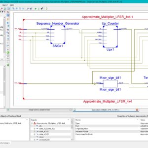
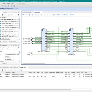
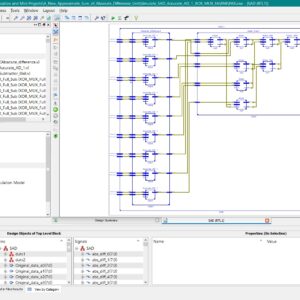
Source : Tanner EDA
Base paper abstract:
Implementation techniques and results for a recently proposed real-time reconfigurable low-pass equalizer (RLPE) consisting of a variable bandwidth (VBW) filter and a variable equalizer (VE) are presented. Both components utilize fixed finite-length impulse response (FIR) filters combined with a few general multipliers, resulting in lower area and power consumption compared to a general FIR filter, despite requiring more multiplications. This is because the constant multipliers in the fixed FIR filters of the RLPE can be optimized for implementation. An additional advantage is that the proposed RLPE does not require online design. Various implementation alternatives for fixed FIR filters, including ways to increase the frequency, are evaluated to optimize the implementation of the RLPE. Several versions of the proposed RLPE and a general FIR filter for comparison are implemented using a 28-nm fully depleted silicon on insulator (FD-SOI) standard cell library. The results demonstrate that the RLPE baseline design requires less power and area than the general equalizer, and although the frequency of the baseline implementation is lower, the design can reach the same frequency while still having significantly less power and area. Furthermore, an approach is introduced to break the chain in the polynomial section of the VBW filter by using fewer additional registers compared to standard pipelining. Instead, this method reformulates the constant multiplication problem to produce correct results. For the considered case, the power consumption is reduced between 49% and 70% for different frequencies, with an area decrease in the range of 64% to 67%, by using the proposed RLPE compared to a general FIR filter. Index Terms: Constant multiplications, real-time reconfiguration, variable bandwidth (VBW) low-pass filter, variable equalizer (VE).
List of the following materials will be included with the Downloaded Backup:
Ultra-low-power analog circuits play a vital role in applications such as Internet of Things devices, wearable electronics, biomedical monitoring systems, and sensor interfaces, where low energy consumption, compact area, and reliable operation at reduced supply voltages are essential advantages. However, these systems also face challenges such as limited voltage headroom, reduced speed, and performance degradation when operating in deep-submicron technologies. Conventional gate-driven OTAs struggle to operate efficiently below 0.5 V, while existing bulk-driven OTAs, although suitable for low-voltage operation, often suffer from low gain, higher delay, and poor robustness. Most reported solutions improve gain or stability at the cost of increased power consumption, larger silicon area, or additional biasing complexity, and comparative studies across advanced CMOS nodes are limited. To address these limitations, this work presents the design of a two-stage operational transconductance amplifier using a bulk-driven technique combined with self-cascode composite transistors and intrinsic current-buffer Miller compensation, implemented in both 45 nm and 22 nm CMOS technologies. The proposed architecture achieves high voltage gain without additional bias voltages, while the intrinsic current-buffer compensation ensures stable frequency response with minimal area overhead. The novelty of this work lies in the systematic comparison of the proposed OTA across 45 nm and 22 nm technologies, highlighting improvements in power consumption, silicon area, and delay achieved through technology scaling while preserving stable operation. The design performance is evaluated using circuit level simulations on Tanner EDA platforms, with key parameters such as gain, power consumption, area, and delay carefully analysed. The results demonstrate that the proposed OTA achieves ultra-low-power operation with improved efficiency and scalability, making it well suited for next-generation low-power analog front-end applications.
” Thanks for Visit this project Pages – Buy It Soon “
Payment Method :
HDFC BANK ACCOUNT:
₹20,000.00 Original price was: ₹20,000.00.₹12,000.00Current price is: ₹12,000.00.


₹16,000.00 Original price was: ₹16,000.00.₹10,000.00Current price is: ₹10,000.00.
Copyright © 2026 Nxfee Innovation.
0.4-V nW-Power High-Gain Bulk-...
₹10,000.00 Original price was: ₹10,000.00.₹6,000.00Current price is: ₹6,000.00.