HDFC BANK ACCOUNT:
- NXFEE INNOVATION,
HDFC BANK, MAIN BRANCH, PONDICHERRY-605004.
INDIA,
ACC NO. 50200090465140,
IFSC CODE: HDFC0000407.

₹10,000.00 Original price was: ₹10,000.00.₹6,000.00Current price is: ₹6,000.00.
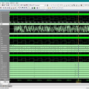
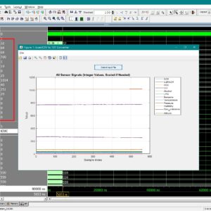
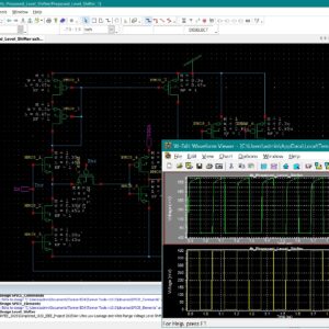
Source : Tanner EDA
Base paper abstract:
This brief presents a 55-nm level shifter (LS) that enables wide voltage range conversion from 80 mV to 1.2 V with high energy efficiency and fast transition speed. The proposed design incorporates a complementary output buffer and an assist discharge path to suppress the short-circuit current and enhance the transition speed. A multi threshold transistor strategy is adopted to expand the input range and reduce static power. Measurement results across 15 samples demonstrate robust subthreshold performance with 4.4-ns transition delay and 49.1-fJ/transition energy during 0.3–1.2-V conversion at 1 MHz. The measured average minimum convertible input voltages are 80 and 139 mV at input frequencies of 50 kHz and 1 MHz, respectively. The compact layout occupies only 7.96 µm 2. Compared to the best benchmarked prior work, the proposed LS achieves 33.8% improvement in energy-delay metrics, making it a highly efficient and scalable solution for energy constrained systems and the Internet of Things (IoT). Index Terms: Current mirror (CM), dual supply, level shifter (LS), low power, subthreshold.
List of the following materials will be included with the Downloaded Backup:
A compact and energy-efficient level shifter is essential in voltage-scaled systems such as low-power processors, sensor nodes, and memory-centric architectures where wide voltage interfacing and fast signal translation are required. Existing level shifters provide good conversion range and moderate delay, but they often suffer from large transistor counts, increased area, higher leakage, and reduced efficiency when operated in deeply scaled technologies. These limitations become more significant in memory-dominated systems, where level shifting directly affects the stability and read performance of SRAM cells. This paper level shifter-based and buffer-assisted structures use 7 to 13 transistors and introduce additional parasitic loading that limits speed and increases dynamic power. To address these issues, this work proposes an optimized and ultra-compact level shifter using only 5 transistors in 45-nm CMOS technology. The design restructures the current mirror and feedback path to reduce short-circuit current, minimize leakage, and preserve a voltage gain of about 6.02 dB while cutting device count by more than half compared to earlier designs. A key novelty of this work is the integration of the proposed level shifter into a 6T SRAM read-assist path, where the amplified output enhances bit line differential swing, improves read stability, and reduces latency without adding substantial area or energy overhead. The proposed circuit is evaluated through schematic-level simulations using Tanner EDA, measuring delay, power, minimum operating voltage, gain, and stability under typical and corner conditions. Results confirm that the five-transistor architecture achieves lower power consumption, reduced delay, and smaller silicon area while improving memory read performance, demonstrating its suitability for compact and energy-constrained system-on-chip applications.
” Thanks for Visit this project Pages – Buy It Soon “
Payment Method :
HDFC BANK ACCOUNT:

₹10,000.00 Original price was: ₹10,000.00.₹8,000.00Current price is: ₹8,000.00.


₹18,000.00 Original price was: ₹18,000.00.₹10,000.00Current price is: ₹10,000.00.
Copyright © 2026 Nxfee Innovation.
A Fast and Energy-Efficient Le...
₹10,000.00 Original price was: ₹10,000.00.₹6,000.00Current price is: ₹6,000.00.