No products in the cart.
Return To ShopHDFC BANK ACCOUNT:
- NXFEE INNOVATION,
HDFC BANK, MAIN BRANCH, PONDICHERRY-605004.
INDIA,
ACC NO. 50200090465140,
IFSC CODE: HDFC0000407.

₹12,000.00 Original price was: ₹12,000.00.₹6,000.00Current price is: ₹6,000.00.
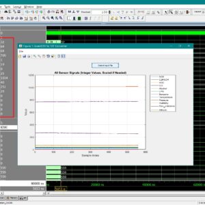
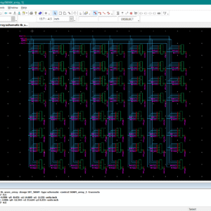
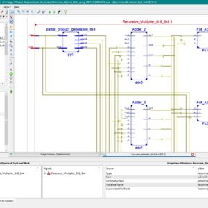
Source : Tanner EDA
From : IEEE Transaction on VLSI System, VOL. 73, NO. 1, JANUARY 2026.
Base paper abstract:
This brief presents a fractional output divider (FOD) with a foreground digital-to-time converter (DTC) INL calibration scheme. This calibration scheme adjusts the delay control words of two main DTCs (mDTCs) to enable mutual comparison between them. By using a sign-least-mean-squares (sign-LMS) algorithm, the INL error codes are obtained and subsequently applied to a calibration DTC (cDTC) to compensate for the mDTC INL. The prototype occupies a compact core area of 0.01mm2 and operates at a 0.9V supply with a power consumption of 3.6mW at 500MHz. Measurements demonstrate an integrated jitter of 512fs (10kHz to 20MHz) and spur level of -70dBc at 123.46MHz. Index Terms—Fractional output divider (FOD), frequency synthesis, digital-to-time converter (DTC), integral nonlinearity (INL), foreground calibration, bang-bang phase detector (BBPD).
List of the following materials will be included with the Downloaded Backup:
Objective:
Proposed abstract:
Fractional output dividers are widely used in system-on-chip applications such as processors, communication systems, data converters, and low-power embedded devices for generating multiple clock frequencies from a single reference source. Compared to conventional multi-PLL clocking systems, fractional output divider based architectures offer advantages such as reduced silicon area, lower power consumption, fast frequency switching, and simpler integration. However, these architectures also suffer from challenges including timing jitter, fractional spurs, and sensitivity to digital-to-time converter nonlinearity, especially when operating at low supply voltages. With the increasing demand for ultra-low-power SoCs, reliable clock generation at reduced voltages has become a critical problem. Existing solutions often rely on auxiliary PLLs, replica DTCs, or complex analog calibration circuits, which increase design complexity, power, and area, and are not well suited for low-voltage operation. In this work, a fractional output divider architecture is proposed and implemented in 45-nm and 65-nm CMOS technology using the Tanner EDA tool, targeting reliable operation at a reduced supply voltage. The proposed design adopts a largely digital, open-loop clocking approach and incorporates DTC gain calibration, offset calibration, and foreground INL calibration to mitigate timing errors under low-voltage conditions. The novelty of this work lies in achieving effective DTC calibration without additional analog loops or auxiliary PLLs, making the design compact and power efficient. The system performance is evaluated through Tanner-based schematic design and T-Spice simulations, focusing on parameters such as power consumption, delay linearity, and jitter behaviour. Simulation results demonstrate acceptable clock quality suitable for SoC applications while achieving reduced power and area, validating the effectiveness of the proposed approach.
” Thanks for Visit this project Pages – Buy It Soon “
Payment Method :
HDFC BANK ACCOUNT:
₹25,000.00 Original price was: ₹25,000.00.₹12,000.00Current price is: ₹12,000.00.


₹20,000.00 Original price was: ₹20,000.00.₹10,000.00Current price is: ₹10,000.00.
Copyright © 2026 Nxfee Innovation.
An Area-Efficient Fractional O...
₹12,000.00 Original price was: ₹12,000.00.₹6,000.00Current price is: ₹6,000.00.