Improvements:
To design and implement a camouflaged logic gate using a threshold voltage defined memory cell in 45 nm CMOS technology in order to reducing power consumption, propagation delay, and area.
To design and analyse data flip-flop and a shift register, using the proposed camouflaged logic gate.
Proposed abstract:
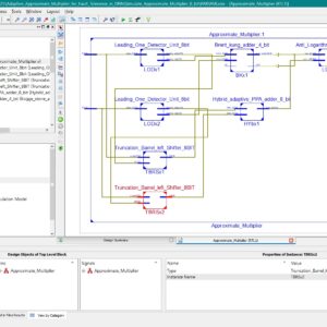
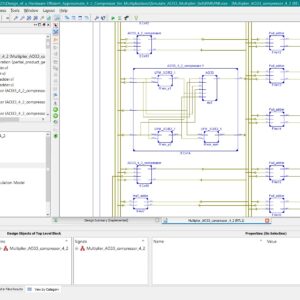
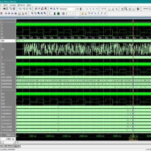
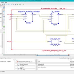
Camouflaged logic circuits are widely used in secure VLSI applications such as defence electronics, cryptographic processors, and intellectual property protection, where resistance to reverse engineering is critical. Threshold-voltage-based camouflaging techniques offer strong security without altering layout patterns, providing advantages such as invisibility to optical inspection and compatibility with standard CMOS processes; however, existing approaches often suffer from increased power consumption, large delay, complex dynamic circuitry, and area overhead. In current research, camouflaged gates based on dynamic threshold-voltage logic and threshold-defined switch designs have been demonstrated, but these methods introduce dynamic power overhead, leakage issues, or degraded performance due to weakly turned-on transistors. To address these limitations, this work proposes the development of a camouflage logic gate using a threshold-voltage-defined memory cell implemented in 45 nm CMOS technology, focusing on reducing power consumption, propagation delay, and silicon area while maintaining strong security against reverse engineering. The proposed design uses static CMOS logic combined with threshold-voltage-defined memory cells to select the intended logic function, eliminating dynamic pre charge operations and minimizing leakage current. In addition, the proposed camouflaged logic gate is extended to design key sequential circuits, including a data flip-flop and a shift register, demonstrating its suitability for practical digital system applications. The novelty of this work lies in integrating low-overhead camouflaged logic into both combinational and sequential circuits using a scalable 45 nm CMOS implementation. Performance evaluation is carried out through schematic design, layout implementation, and post-layout simulations using Tanner EDA tools, where parameters such as power consumption, delay, area, and leakage current are analysed and compared with conventional designs to validate the effectiveness of the proposed approach.
Software Implementation:
- Tanner EDA
” Thanks for Visit this project Pages – Buy It Soon “
Design of Low Power Threshold Voltage Based Camouflaging Technique for Secure Combinational and Sequential VLSI Circuits
Terms & Conditions:
- Customer are advice to watch the project video file output, before the payment to test the requirement, correction will be applicable.
- After payment, if any correction in the Project is accepted, but requirement changes is applicable with updated charges based upon the requirement.
- After payment the student having doubts, correction, software error, hardware errors, coding doubts are accepted.
- Online support will not be given more than 3 times.
- On first time explanations we can provide completely with video file support, other 2 we can provide doubt clarifications only.
- If any Issue on Software license / System Error we can support and rectify that within end of the day.
- Extra Charges For duplicate bill copy. Bill must be paid in full, No part payment will be accepted.
- After payment, to must send the payment receipt to our email id.
- Powered by NXFEE INNOVATION, Pondicherry.
Payment Method :
- Pay Add to Cart Method on this Page
- Deposit Cash/Cheque on our a/c.
- Pay Google Pay/Phone Pay : +91 9789443203
- Send Cheque through courier
- Visit our office directly
- Pay using Paypal : Click here to get NXFEE-PayPal link
Bank Accounts
HDFC BANK ACCOUNT:
- NXFEE INNOVATION,
HDFC BANK, MAIN BRANCH, PONDICHERRY-605004.
INDIA,
ACC NO. 50200090465140,
IFSC CODE: HDFC0000407.