HDFC BANK ACCOUNT:
- NXFEE INNOVATION,
HDFC BANK, MAIN BRANCH, PONDICHERRY-605004.
INDIA,
ACC NO. 50200090465140,
IFSC CODE: HDFC0000407.

₹25,000.00 Original price was: ₹25,000.00.₹16,000.00Current price is: ₹16,000.00.
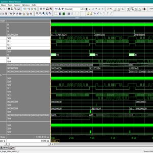
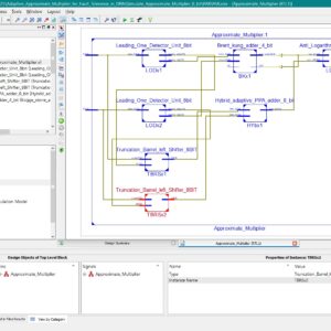
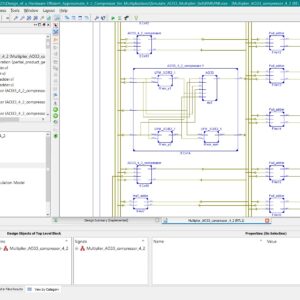
Source : Verilog HDL
Base paper abstract:
Fail-safe computing refers to computing systems that revert to a non-operational safe state when a fault occurs. In this paper, we investigate a circuit level technique as mitigation for single event upsets (SEUs) and fault injection attacks on field programmable gate arrays (FPGAs), and analyze the effectiveness of the technique as a fail-safe monitor for an encryption algorithm. The propagation of fault effects through FPGA primitives including lookup tables (LUTs) and programmable interconnect points (PIPs) is assessed within an FPGA architecture created using an open source tool, and validated using fault injection experiments on an FPGA. The analysis reveals additional vulnerabilities exist within reconfigurable architectures over those in equivalent fail-safe application specific integrated circuit (ASIC), thus requiring a more elaborate network of redundant circuits and checking logic. The configuration memory bits (CMBs), which configure routing and designate logic functions within the LUTs of the FPGA, add complexity to fail-safe design strategies by introducing additional fault conditions and fault propagation paths. A resource efficient fail-safe circuit design technique called Design for Fail-safe in reconfigurable systems (DEFCON) is proposed. The benefits and limitations associated with DEFCON are described in the context of fault injection experiments carried out as simulations and in FPGA hardware.
List of the following materials will be included with the Downloaded Backup:
Objectives of the Proposed Work
Proposed abstract:
Fail-safe architectures are increasingly required in safety-critical and security-critical FPGA applications such as cryptographic accelerators, automotive controllers, and industrial control systems, where any fault must be detected and the system must transition into a known safe state rather than continue operation. These architectures offer strong protection against configuration memory upsets, routing faults, and malicious fault injection attacks, but they typically suffer from increased area overhead, complex monitoring logic, and limited support for runtime recovery. Existing FPGA-based solutions mainly rely on triple modular redundancy or basic duplication-with-comparison techniques, which either incur high resource costs or lack self-checking capability within the monitoring circuitry itself. Moreover, many prior works validate fail-safe concepts using abstract FPGA models or SoC-based platforms, with limited evidence of full Verilog-based dynamic partial reconfiguration implementation on low-cost standalone FPGAs. To address these limitations, this work proposes a complete DEFCON-inspired fail-safe architecture implemented entirely in synthesizable Verilog HDL using a dynamic partial reconfiguration region on an Artix-7 FPGA. Two redundant instances of an AES-128 cryptographic core operate synchronously within the DPR region, while compact self-checking monitors detect mismatches in internal datapath registers and output interfaces. The proposed solution exploits the dual-output structure of FPGA LUTs to realize resource-efficient redundant XOR and OR comparison logic, ensuring that faults within the monitoring circuitry itself do not mask functional faults. A hierarchical alarm generation and compression network guarantees reliable fault detection under single-fault and selected dual-fault conditions, and a fail-safe output blocking mechanism enforces a predefined safe output state. The novelty of this work lies in the practical realization of a reusable, Verilog-only fail-safe DPR framework on a standalone FPGA with quantified timing, area, and power results. The design is synthesized and implemented using Xilinx Vivado, achieving timing closure with positive slack, low resource utilization, and modest power consumption, thereby demonstrating the feasibility and effectiveness of the proposed architecture for real-world fail-safe FPGA systems.
” Thanks for Visit this project Pages – Buy It Soon “
Payment Method :
HDFC BANK ACCOUNT:
₹16,000.00 Original price was: ₹16,000.00.₹10,000.00Current price is: ₹10,000.00.


₹16,000.00 Original price was: ₹16,000.00.₹10,000.00Current price is: ₹10,000.00.
Copyright © 2026 Nxfee Innovation.
Fail Safe Logic Design Strateg...
₹25,000.00 Original price was: ₹25,000.00.₹16,000.00Current price is: ₹16,000.00.