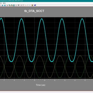
0.4-V nW-Power High-Gain Bulk-Driven Two-Stage OTA With Self-Cascode Composite Transistors
Implementation techniques and results for a recently proposed real-time reconfigurable low-pass equalizer (RLPE) consisting of a variable bandwidth (VBW) filter and a variable equalizer (VE) are presented. Both components utilize fixed finite-length impulse response (FIR) filters combined with a few general multipliers, resulting in lower area and power consumption compared to a general FIR filter, despite requiring more multiplications. This is because the constant multipliers in the fixed FIR filters of the RLPE can be optimized for implementation. An additional advantage is that the proposed RLPE does not require online design. Various implementation alternatives for fixed FIR filters, including ways to increase the frequency, are evaluated to optimize the implementation of the RLPE. Several versions of the proposed RLPE and a general FIR filter for comparison are implemented using a 28-nm fully depleted silicon on insulator (FD-SOI) standard cell library. The results demonstrate that the RLPE baseline design requires less power and area than the general equalizer, and although the frequency of the baseline implementation is lower, the design can reach the same frequency while still having significantly less power and area. Furthermore, an approach is introduced to break the chain in the polynomial section of the VBW filter by using fewer additional registers compared to standard pipelining. Instead, this method reformulates the constant multiplication problem to produce correct results. For the considered case, the power consumption is reduced between 49% and 70% for different frequencies, with an area decrease in the range of 64% to 67%, by using the proposed RLPE compared to a general FIR filter. Index Terms: Constant multiplications, real-time reconfiguration, variable bandwidth (VBW) low-pass filter, variable equalizer (VE).
List of the following materials will be included with the Downloaded Backup: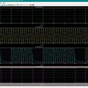
A 25-Mb/s 4-ASK Receiver Front-End in 65-nm CMOS for Biomedical Data Telemetry via a Capacitive Link
This brief presents a 25-Mbps 4-amplitude-shiftkeying (4-ASK) receiver front-end (RFE) for biomedical data telemetry via a series-resonant capacitive link. The RFE incorporates low-power clock and data recovery (CDR) circuitry for synchronization in which a novel highly linear trans conductance (Gm) cell is employed in the phase detector (PD) to mitigate any possible error decisions while comparing the phase difference between the input and feedback signals. The proposed RFE is fabricated in 65 nm 1P8M standard CMOS, the core circuit occupies 0.11 mm2, and consumes 2.9 mA from 1 V. While conducting ex vivo measurements using beef tissue and a series-resonant capacitive link, the proposed RFE is capable of processing 4-ASK data patterns up to 25 Mbps with bit error rate (BER) less than 10−3 and total jitter of ∼42 ns. Index Terms Amplitude-shift-keying (ASK), capacitive wireless data transfer (C–WDT), clock and data recovery (CDR), receiver front-end (RFE), series-resonant capacitive link.
List of the following materials will be included with the Downloaded Backup: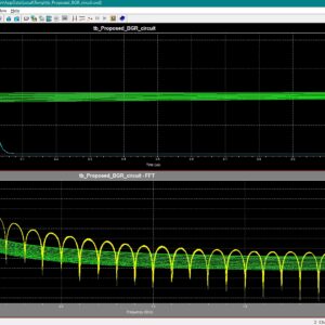
A 57.2 nW, 1.3–5 V V IN, –85 dB PSRR, 50 µs Start-Up Time, Bandgap Reference Circuit
This article presents a low-power bandgap reference (BGR) featuring high power supply rejection ratio (PSRR) and fast start-up capability, operating across a wide supply voltage range of 1.3–5 V. A novel pre biased pulse current injection technique is proposed in the start-up circuit, achieving a 1% settling time of 50 µs and a 25× speed gain during start-up. To enhance supply noise immunity, the proposed BGR employs a pre regulated (PR)-based amplifier that effectively decouples the reference voltage from supply voltage fluctuations. Fabricated in a 0.18-µm BCD process, the proposed reference occupies an active area of 0.0394 mm 2. Under a 5 V supply, the circuit generates a 1.2 V reference voltage while consuming only 48 nA quiescent current. Operating down to a minimum supply voltage of 1.3 V, it maintains a low power consumption of 57.2 nW at room temperature. The reference exhibits an average temperature coefficient (TC) of 5.95 ppm/◦C across a wide temperature range (−40◦C to 125◦C) and achieves an outstanding line sensitivity (LS) of 0.00308%/V over the 1.3–5 V supply range. Furthermore, the measured PSRR reaches −85 dB at 100 Hz. Index Terms: Bandgap reference (BGR), pre bias pulse current injection, power supply rejection ratio (PSRR), start-up, ultralow-power (ULP).
List of the following materials will be included with the Downloaded Backup:
A 9T SRAM Computation-in-Memory Architecture with High-Precision MAC
To address the data-intensive demands of modern artificial intelligence (AI) systems, computation-in-memory(CIM) based on static random-access memory (SRAM) has emerged as a promising solution by integrating computing functionality within memory arrays. However, conventional SRAM CIM architectures face two key limitations: low output resistance in single-transistor transmission paths and voltage instability on charge-sharing bitlines. These limitations collectively degrade computational accuracy to 4–5 LSB-level integral nonlinearity (INL), restricting practical deployment. This work proposes a regulated-cascode 9T SRAM cell that enhances analog computation accuracy using a high-impedance transmission path through a cascode configuration and stabilizing the discharge amount of the bitline from a single cell via active feedback regulation. Implemented in Semiconductor Manufacturing International Corporation (SMIC) 55-nm CMOS technology, the proposed cell demonstrates 1.31 LSB INL at 400-mV bitline swing (68.4% improvement versus 4–5 LSB baselines), achieving 66.7% voltage utilization efficiency compared with the conventional 50% limit and 23.04% frequency improvement is achieved compared with the conventional architecture. It also achieves an energy efficiency of 18.47 fJ/bit and a compact area of 2.655 × 1.175 µm, while demonstrating a classification accuracy of 97.7% on the MNIST dataset. Index Terms Analog linearity enhancement, multirow readout, regulated cascode circuits, static random-access memory (SRAM)-based compute-in-memory, voltage utilization efficiency.
List of the following materials will be included with the Downloaded Backup: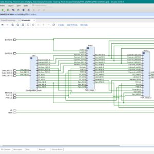
A Configurable Floating-Point Fused Multiply-Add Design with Mixed Precision for AI Accelerators
Base Paper Abstract:
Hardware accelerators for deep learning in artificial intelligence applications must often meet stringent constraints for accuracy and throughput. In addition to architecture/algorithm improvements, high performance computational techniques such as mixed precision are also required. In this paper, a floating-point (FP) fused multiply-add (FMA) unit supporting mixed/multiple precision is proposed. A wide range of conventional FP formats (such as half and single) as well as emerging formats (including E4M3, E5M2, DLFloat, BFLoat16 and TF32) are supported in the proposed design. In addition to all these formats, the proposed design is flexible in manipulating the exponent and mantissa lengths for 8, 16 and 32-bit FP numbers based on the needs of an application. The proposed FMA can be configured to support either multiple normal FMA operations, or alternatively mixed precision in ASIC. It is fully pipelined and in each cycle, the input bit streams are processed based on the provided configuration, so independent of the previous cycles. For normal FMA operations, the proposed design utilizes sharing of resources to parallelize multiple operations based on the available hardware and required precision. For mixed precision the FMA accumulates the lower precision dot products into higher precision to avoid overflow/underflow. It improves computational accuracy by adding all possible dot products at the same time while decreasing the number of rounding operations to prevent rounding errors. An innovative method to accumulate the dot products and the aligned addend is also proposed. By, considering tradeoffs between reusing the available hardware and removing unnecessary complex units, a more efficient and flexible design is attained in terms of hardware metrics and supported different precision computation compared to other designs found in the technical literature. Extensive simulation results for comparative analysis are provided.
List of the following materials will be included with the Downloaded Backup:
A Design of lightweight true random number generator based on Galois LFSR with dynamic feedback path
Base Paper Abstract:
The Linear Feedback Shift Register (LFSR) is a widely utilized circuit structure in electronic systems, often employed as a Pseudo Random Number Generator (PRNG) for generating pseudo random sequence. However, in light of the significant challenges associated with privacy protection and data encryption, traditional PRNGs have frequently failed to meet the increasing security demands of electronic systems. In contrast, True Random Number Generators (TRNGs), have emerged as essential security primitives within the realm of hardware security, garnering increasing attention. In response to these challenges, this paper proposes a novel lightweight TRNG architecture based on Galois LFSR. This innovation design incorporates inverters and two-to-one multiplexers to modify the feedback path. The proposed structure has been implemented on AMD Xilinx Artix-7 and Kintex-7 FPGA boards. Notably, it demonstrates a resource-efficient design, utilizing only 17 Look-Up Tables (LUTs) and 9 D Flip-Flops (DFFs), while achieving random number with throughput of 300Mbps. Furthermore, the structure successfully passes both randomness test and robustness test, indicating its promising application potential in secure electronic systems.
List of the following materials will be included with the Downloaded Backup:
A Fast and Energy-Efficient Level Shifter with Complementary Output Buffer for Energy-Constrained Systems
This brief presents a 55-nm level shifter (LS) that enables wide voltage range conversion from 80 mV to 1.2 V with high energy efficiency and fast transition speed. The proposed design incorporates a complementary output buffer and an assist discharge path to suppress the short-circuit current and enhance the transition speed. A multi threshold transistor strategy is adopted to expand the input range and reduce static power. Measurement results across 15 samples demonstrate robust subthreshold performance with 4.4-ns transition delay and 49.1-fJ/transition energy during 0.3–1.2-V conversion at 1 MHz. The measured average minimum convertible input voltages are 80 and 139 mV at input frequencies of 50 kHz and 1 MHz, respectively. The compact layout occupies only 7.96 µm 2. Compared to the best benchmarked prior work, the proposed LS achieves 33.8% improvement in energy-delay metrics, making it a highly efficient and scalable solution for energy constrained systems and the Internet of Things (IoT). Index Terms: Current mirror (CM), dual supply, level shifter (LS), low power, subthreshold.
List of the following materials will be included with the Downloaded Backup: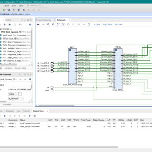
A Pipelined Fused Multiply-Add Architecture for Configurable FP16 Multi-Operand Operations
Base Paper Abstract:
Multiple precision modes are needed for a floating-point processing element (PE) because they provide flexibility in handling different types of numerical data with varying levels of precision and performance metrics. Performing high-precision floating-point operations has the benefits of producing highly precise and accurate results while allowing for a greater range of numerical representation. Conversely, low-precision operations offer faster computation speeds and lower power consumption. In this paper, we propose a configurable multi-precision processing element (PE) which supports Half Precision, Single Precision, Double Precision, BrainFloat-16 (BF-16) and TensorFloat-32 (TF-32). The design is realized using GPDK 45 nm technology and operated at 281.9 MHz clock frequency. The design was also implemented on Xilinx ZCU104 FPGA evaluation board. Compared with previous state-of-the-art (SOTA) multiprecision PEs, the proposed design supports two more floating point data formats namely BF-16 and TF-32. It achieves the best energy performance with 2368.91 GFLOPS/W and offers 63% improvement in operating
List of the following materials will be included with the Downloaded Backup: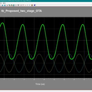
A Two-Stage CMOS Amplifier with High Degree of Stability for All Capacitive Loads
This article presents the conception, design, and realization of a fully differential two-stage CMOS amplifier, that is, unconditionally stable for any value of the capacitive load. This is simply achieved by sending a scaled replica of the output stage current to the amplifier virtual ground in order to create a left half-plane (LHP) zero in the loop gain that either cancels or tracks the output pole in all process, voltage, and temperature (PVT) conditions. Consequently, from a stability point of view, the amplifier behaviour resembles that of a single-pole OTA. Starting from an existing two-stage gain-programmable amplifier, designed in a 0.18-µm bipolar-CMOS-DMOS (BCD) process that was able to drive only 10 pF without encountering into stability issues, a simple circuit has been added to extend the stability to any capacitive load value. An interesting and unusual method, based on the frequency behaviour of the unloaded closed-loop amplifier output impedance, has been introduced to further verify the unconditional stability of this solution. Measurements show a high degree of stability in any load conditions. In the used 0.18-µm BCD technology, silicon area and current consumption of the extra circuit are only 0.0004 mm and 2 µA, respectively, with a 5-V power supply.
List of the following materials will be included with the Downloaded Backup: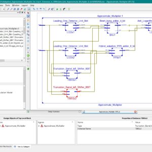
AdAM: Adaptive Approximate Multiplier for Fault Tolerance in DNN Accelerators
Base Paper Abstract:
Deep Neural Network (DNN) hardware accelerators are essential in a spectrum of safety-critical edge-AI applications with stringent reliability, energy efficiency, and latency requirements. Multiplication is the most resource-hungry operation in the neural network’s processing elements. This paper proposes a scalable adaptive fault-tolerant approximate multiplier (AdAM) tailored for ASIC-based DNN accelerators at the algorithm and circuit levels. AdAM employs an adaptive adder that relies on an unconventional use of input Leading One Detector (LOD) values for fault detection by optimizing unutilized adder resources. A gate-level optimized LOD design and a hybrid adder design are also proposed as a part of the adaptive multiplier to improve the hardware performance. The proposed architecture uses a lightweight fault mitigation technique that sets the detected faulty bits to zero. The hardware resource utilization and the DNN accelerator’s reliability metrics are used to compare the proposed solution against the Triple Modular Redundancy (TMR) in multiplication, unprotected exact multiplication, and unprotected approximate multiplication. It is demonstrated that the proposed architecture enables a multiplication with a reliability level close to the multipliers protected by TMR while at the same time utilizing 2.74× less area and with 39.06% less power-delay product compared to the exact multiplier. Moreover, it has similar area, delay, and power consumption parameters compared to the state-of-the-art approximate multipliers with similar accuracy while providing fault detection and mitigation capability. Index Terms Deep neural networks, approximate computing, circuit design, reliability, DNN accelerator.
List of the following materials will be included with the Downloaded Backup:
An Efficient Approximate Sum of Absolute Differences Hardware for FPGAs
Proposed Abstract:
Sum of Absolute Differences (SAD) is mainly applied in block-matching tasks such as motion estimation for video compression, stereo matching for depth/disparity calculation, template matching in image/object detection, image registration (including medical imaging), and lightweight optical-flow/tracking systems, because it is simple, fast, and hardware-friendly. The Traditional accurate SAD hardware provides exact results but consumes high power and requires large area, while existing approximate designs reduce cost but often suffer from high errors and poor FPGA-specific optimization. To overcome these limitations, this work proposes an improved SAD hardware architecture that replaces the conventional full adder with a lightweight XOR–MUX structure. This change reduces delay, minimizes area, and increases speed by removing redundant logic and optimizing FPGA resource utilization. The novelty of the design lies in combining approximation with FPGA-aware optimization, achieving bounded error, reduced power consumption, and higher operating frequency. The proposed system is implemented in Verilog HDL and tested on a Xilinx FPGA, showing improvements in LUT usage, clock frequency, and power efficiency, making it suitable for real-time video and image processing applications.
List of the following materials will be included with the Downloaded Backup:
An Ultra-Low Leakage and Wide-Range Voltage Level Shifter for Low-Power Digital CMOS VLSIs
Base Paper Abstract:
This brief presents an ultra-low leakage and fast conversion level shifter with wide-range voltage conversion and frequency. The proposed level shifter adopts the leakage shutoff transistors, which can completely cut off the static current when the circuits stand by. The pull-down network employs the low-threshold transistor for the fast fall transition. The proposed level shifter also solves the swing problem and achieves a fast conversion by using the voltage hysteresis transistor, strengthening the pull-up network to ensure the internal node is fast and fully charged. Measurement results based on the 55 nm process show that the average ultra-low leakage of the proposed level shifter is 34.8 pW when converting from 0.3 V input to 1.2 V output. Meanwhile, the average propagation delay and the average energy per transition of the proposed level shifter are 13.86 ns and 22.71 fJ for an input frequency of 1 MHz, respectively. The maximum conversion range is from 0.13 V to 1.2 V. Index Terms: Level shifter, ultra-low power, multi-supply voltage circuit, sub-threshold operation.
List of the following materials will be included with the Downloaded Backup: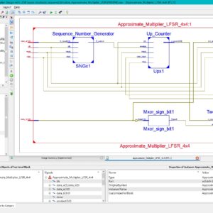
Approximate Multiplier Design with LFSR-Based Stochastic Sequence Generators for Edge AI
Base Paper Abstract:
This letter introduces an innovative approximate multiplier (AM) architecture that leverages stochastically generated bit streams through the Linear Feedback Shift Register (LFSR). The AM is applied to matrix-vector multiplication (MVM) in Neural Networks (NNs). The hardware implementations in 90 nm CMOS technology demonstrate superior power and area efficiency compared to state-of-the-art designs. Additionally, the study explores applying stochastic computing to LSTM NNs, showcasing improved energy efficiency and speed.
List of the following materials will be included with the Downloaded Backup:
Camouflaged Logic Gates Using Threshold-Voltage-Defined Memory Cells
This brief proposes two types of camouflaged logic gates using threshold-voltage-defined memory cells (TVD-MCs). The proposed multiplexer-select TVD-MC (MS-TVDMC) gate consists of a target logic gate, several camouflage logic gates, a multiplexer (MUX), and TVD-MCs. All logic gates and MUX are implemented with standard threshold-voltage transistors. The TVD-MC is composed of two cross coupled inverters with low- or high-threshold-voltage transistors. When its supply voltage increases from ground to VDD, its data become “0” or “1” according to the threshold voltages of transistors in two inverters. The target logic gate is selected with the MUX by the data stored in the TVD-MCs. The data are defined by the threshold voltages of transistors, so that it is difficult to distinguish the target logic gate from the other camouflage logic gates. The proposed logic-merged TVD-MC (LM-TVDMC) gate merges all logic gates and MUX in the MS-TVDMC gate at the transistor level. The proposed camouflaged gates significantly reduce the delay, power consumption, and leakage current compared to the conventional dynamic enhanced-TVD (DE-TVD) camouflaged gate requiring the dynamic power and delay overheads and the conventional threshold-voltage-defined (TVD) switch camouflaged gate with large ON-resistances in switch transistors. Index Terms: Camouflaged gate, logic gate, reverse engineering, security, threshold-voltage-defined (TVD).
List of the following materials will be included with the Downloaded Backup:
Design and Analysis of Energy Efficient Approximate Multipliers for Image Processing and DNN
Base Paper Abstract:
Numerous obstacles in enhancing the performance of computing systems have spurred the emergence of approximate computing. Extensive studies have been reported on approximate computing to develop high-performance, energy-efficient hardware designs tailored to error-resilient applications. In this brief, we proposed 8-bit approximate multipliers with 15 levels of accuracy using three techniques: recursive, bit-wise, and hybrid approximation using partial bit OR (PBO). Compared to the existing multipliers, investigated designs have significantly improved the area, power, delay, Power Delay Product (PDP), and Power Area Delay Product (PADP) by 41.68%, 73.16%, 35.57%, 72.65%, and 75.42% respectively on average. On resemblance with the accurate multiplier, the area, power, delay, PDP, and PADP were enhanced by 54.41%, 57.57%, 25.73%, 60.14%, and 74.33% correspondingly on average. Peak Signal-to-Noise Ratio (PSNR) and Structural Similarity Index Measure (SSIM) values surpassing (30 dB, 94%), (31 dB, 96%), and (26 dB, 95%) by applying them to benchmarks in image smoothing, edge detection, and image sharpening successively. Moreover, upon scrutinizing the efficacy of multipliers in hardware implementations of deep neural networks attaining the performance exceeding 95%. The obtained results confirm that suggested multipliers are well-suited for their widespread applications.
List of the following materials will be included with the Downloaded Backup:
Design and analysis of Reversible Approximate Full Adder and its applications with Optimized 4:2, 5:2, 7:2 Compressors for Efficient Approximate Multipliers
Design and Implementation of a Low-Complexity Continuously Variable Digital Filter
Base Paper Abstract:
Variable filters with adjustable bandwidth are vital components in diverse communication scenarios. This paper presents an innovative architecture for a continuously variable bandwidth filter using a fixed hardware. Our approach integrates a fixed finite impulse response filter between two arbitrary fractional delay filters implemented through a novel Farrow Equivalent-Newton structure. The proposed architecture provides a low-complexity implementation structure compared to the state-of-the-art approaches. A precise mapping equation for the edge frequencies of the filters generated from the proposed continuously variable bandwidth filter, in terms of a variable parameter called the resampling ratio, is also formulated. Validation experiments encompass the design of continuously variable bandwidth filters tailored to various wireless communication standards. The hardware utilisation report of the proposed continuously variable bandwidth filter obtained by synthesising the structure using Xilinx Vivado 2020.2 on a Kintex-7 device is also included, which proves the hardware complexity reduction and efficiency of the proposed structure.
List of the following materials will be included with the Downloaded Backup: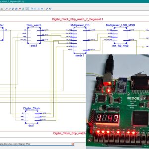
Design and Implementation of a Unified Digital Clock and Stopwatch System Using FSM and Multiplexed Seven-Segment Display
Proposed Abstract:
Digital clocks and stopwatches are widely used in daily applications such as consumer electronics, embedded devices, portable medical instruments, and time monitoring systems, as they provide simple and accurate time tracking functions. These systems offer advantages like low cost, user-friendly operation, and high reliability; however, they often face disadvantages such as hardware redundancy, higher power consumption, and limited integration when clock and stopwatch functions are implemented separately. The main problem addressed in this work is the lack of a unified architecture that can perform both digital clock and stopwatch operations using shared resources, which leads to inefficient hardware utilization and increased complexity in existing designs. Conventional systems generally use independent controllers and dedicated display drivers, resulting in additional overhead. To overcome this limitation, we propose a finite state machine based architecture that integrates both digital clock and stopwatch modules into a single design with common display hardware. The system employs multiplexers and control signals to switch seamlessly between clock and stopwatch modes, while states such as idle, hour, minute, second, and pause are clearly managed through FSM logic. The novelty of this work lies in the resource-sharing approach where a common seven-segment display is driven by multiplexed outputs, thereby reducing area, power, and switching complexity without compromising accuracy. The proposed design is implemented and tested using hardware description language coding and simulated on FPGA-based platforms, ensuring precise timing, functional correctness, and display reliability. Performance evaluation confirms that the system achieves efficient utilization of logic resources, accurate real-time operation, and flexibility for future extension in low-power VLSI and IoT-based applications.
List of the following materials will be included with the Downloaded Backup:
Design of a Hardware Efficient Approximate 4-2 Compressor for Multiplication in Image Processing
Base Paper Abstract:
This letter presents a novel hardware-efficient approximate 4-2 compressor design that significantly enhances accuracy through a systematic analysis of input patterns obtained from practical applications. We incorporate a majority operation and a compound gate in the compressor design to effectively boost hardware efficiency in multiplications. Our design approach results in substantial error reductions, with normalized mean error distance (NMED) and mean relative error distance (MRED) decreasing by up to 74.84% and 82.04%, respectively, compared to existing approximate multipliers discussed in this letter. When implemented in a 32-nm CMOS technology, the approximate multiplier adopting the proposed 4-2 compressor achieves excellent hardware efficiency, reducing area, power, and energy consumption by up to 8.95%, 13.02%, and 13.02%, respectively, compared to the other alternatives. Moreover, our design delivers enhanced performance in image processing tasks, achieving up to a 4.84× increase in peak signal-to-noise ratio (PSNR) compared to other designs, all while optimizing hardware efficiency. Index Terms—Approximate multiplier, majority operation, compound gate, image processing, approximate 4-2 compressor.
List of the following materials will be included with the Downloaded Backup:
Design of a Low-Power Analog Integrated Deep Convolutional Neural Network
Base Paper Abstract:
In this article, a framework for the analog implementation of a deep convolutional neural network (CNN) is introduced and used to derive a new circuit architecture which is composed of an improved analog multiplier and circuit blocks implementing the ReLU activation function and the argmax operator. The operating principles of the individual blocks, as well as those of the complete architecture, are analysed and used to realize a low-power analog classifier, consuming less than 1.8 µW. The proper operation of the classifier is verified via a comparison with a software equivalent implementation and its performance is evaluated against existing circuit architectures. The proposed architecture is implemented in a TSMC 90-nm CMOS process and simulated using Cadence IC Suite for both schematic and layout design. Corner and Monte Carlo mismatch simulations of the schematic and the physical circuit (post layout) were conducted to evaluate the effect of transistor mismatches and process voltage temperature (PVT) variations and to showcase a proposed systematic method for offsetting their effect.
List of the following materials will be included with the Downloaded Backup: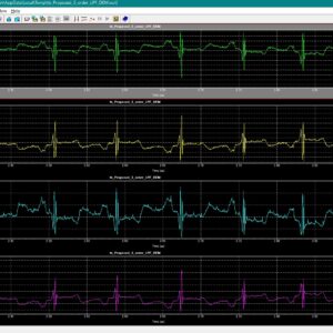
Design of Low-Power and Area Efficient ECG Low Pass Filter Using VSCP
Electrocardiogram (ECG) signal processing is a core requirement in wearable and portable healthcare systems, where long battery life, compact hardware, and reliable signal quality are increasingly demanded by modern medical applications. The aim of this work is to address the challenge of designing an energy-efficient and area-optimized ECG low-pass filter capable of suppressing high-frequency noise while preserving diagnostically important cardiac information in advanced CMOS technology. To achieve this, a low-pass filter based on a vertical source-coupled pair (VSCP) transconductance architecture is proposed, in which the circuit topology and biasing strategy are carefully optimized to suit ECG signal bandwidth and low-voltage operation. The architectural novelty of this work lies in the adaptation and refinement of a VSCP-based transconductance structure into an ECG-specific low-pass filter with reduced transistor count, improved linearity, and enhanced power efficiency in a 45-nm CMOS process. The proposed filter supports essential ECG signal conditioning functions, including low-frequency passband preservation, effective attenuation of out-of-band noise, and stable operation under low-power constraints. The design is implemented and simulated using Tanner EDA tools, and realistic ECG input signals generated from the MIT-BIH database are applied to validate functional performance. Simulation results demonstrate that the proposed filter achieves notable reductions in power consumption and silicon area compared to conventional ECG low-pass filter designs, while maintaining reliable frequency response and low noise, making it well suited for compact and battery-operated ECG monitoring systems.
List of the following materials will be included with the Downloaded Backup:
Energy Efficient Compact Approximate Multiplier for Error-Resilient Applications
Base Paper Abstract:
The primary goal of approximate computing is enhancing system performance, such as energy efficiency, speed, and form factor. Despite the growing use of approximate multipliers, the design of efficient approximate compressors — a fundamental multiplier block — remains a significant challenge. In this brief, 8-transistor and 14-transistor 4:2 compressors are proposed. Both compressors exploit CMOS technology and a constant and conditional approximation of selected inputs, exhibiting fewer negative errors. As a result, a resource-expensive error recovery module is eliminated, yielding superior performance as compared with prior art. The 14-transistor architecture yields a lower error rate compared to the 8-transistor architecture, trading off lower area for higher accuracy. The compressor tailored circuit architecture is also proposed and evaluated using image multiplication. The proposed multiplier exhibits 50% area savings and 93% lower power-delay-product compared to the exact multiplier, as well as higher accuracy, and 38% PDP enhancement compared with the state-of-the-art.
List of the following materials will be included with the Downloaded Backup:
Energy-Efficient Buffer-Based Ternary SRAM Cell With Application to Image Processing
Base Paper Abstract:
This paper presents a design of a variation-resilient and energy-efficient ternary memory cell (TSRAM) suited for power-demanding internet-of-things (IoT) applications that run on batteries. The TSRAM cell utilizes a latch composed of an efficient ternary buffer (TBUF) with positive feedback, a single bit line, and a transmission gate for switching access, with an overall area only about 39% more than binary 6T SRAM. The threshold voltage (Vth) tuning of carbon nanotube field-effect transistor (CNTFET) devices has been explored to achieve the three storage levels. Simulations were conducted using the standard Stanford 32-nm CNTFET model file in the Synopsis HSPICE simulator. The projected design offers substantial reductions of 54.94% in real power, 67.06% in write power, and 21.59% in area compared to the best buffer-based TSRAM designs. These power savings are achieved by minimizing the transistor count and eliminating any direct current path between VDD and ground in the TBUF design for getting logic ‘1’. Furthermore, the proposed design demonstrates the highest logic ‘1’ static noise margin (SNM1) and shows resilience to process, voltage, and temperature (PVT) variations. The TSRAM electrical quality matrix (TEQM), a crucial figure of merit, indicates the superior performance of the proposed design for IoT applications. The study was further extended to conduct simulations and report the performance metrics of the proposed TSRAM array. Ultimately, to evaluate the real-world application of the triple memory structures, the pixel-by-pixel storage process of a grayscale image with three-value data content is performed based on a hardware algorithm. The obtained results demonstrate that the proposed TSRAM architecture has about a 26.3% improvement in hardware performance compared to its highest performing counterpart scheme.
List of the following materials will be included with the Downloaded Backup:
Fail Safe Logic Design Strategies Within Modern FPGA Architectures
Fail-safe computing refers to computing systems that revert to a non-operational safe state when a fault occurs. In this paper, we investigate a circuit level technique as mitigation for single event upsets (SEUs) and fault injection attacks on field programmable gate arrays (FPGAs), and analyze the effectiveness of the technique as a fail-safe monitor for an encryption algorithm. The propagation of fault effects through FPGA primitives including lookup tables (LUTs) and programmable interconnect points (PIPs) is assessed within an FPGA architecture created using an open source tool, and validated using fault injection experiments on an FPGA. The analysis reveals additional vulnerabilities exist within reconfigurable architectures over those in equivalent fail-safe application specific integrated circuit (ASIC), thus requiring a more elaborate network of redundant circuits and checking logic. The configuration memory bits (CMBs), which configure routing and designate logic functions within the LUTs of the FPGA, add complexity to fail-safe design strategies by introducing additional fault conditions and fault propagation paths. A resource efficient fail-safe circuit design technique called Design for Fail-safe in reconfigurable systems (DEFCON) is proposed. The benefits and limitations associated with DEFCON are described in the context of fault injection experiments carried out as simulations and in FPGA hardware.
List of the following materials will be included with the Downloaded Backup:
FPGA Implementation for Odor Identification with Depthwise Separable Convolutional Neural Network
Base Paper Abstract:
The integrated electronic nose (e-nose) design, which integrates sensor arrays and recognition algorithms, has been widely used in different fields. However, the current integrated e-nose system usually suffers from the problem of low accuracy with simple algorithm structure and slow speed with complex algorithm structure. In this article, we propose a method for implementing a deep neural network for odor identification in a small-scale Field-Programmable Gate Array (FPGA). First, a lightweight odor identification with depthwise separable convolutional neural network (OIDSCNN) is proposed to reduce parameters and accelerate hardware implementation performance. Next, the OI-DSCNN is implemented in a Zynq-7020 SoC chip based on the quantization method, namely, the saturation-flooring KL divergence scheme (SF-KL). The OI-DSCNN was conducted on the Chinese herbal medicine dataset, and simulation experiments and hardware implementation validate its effectiveness. These findings shed light on quick and accurate odor identification in the FPGA.
List of the following materials will be included with the Downloaded Backup: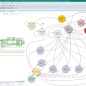
FPGA Implementation of Intelligent Elevator System for AI Applications
Proposed Abstract:
Intelligent elevator systems are used in many smart buildings, offices, hospitals, and tall apartments to move people quickly, reduce waiting time, and save energy. They have many advantages, like faster operation, better safety, and the ability to handle requests from many floors at the same time. But there are also some disadvantages, such as slow response when many people use them, fixed movement patterns that cannot adjust to real-time needs, weak security for restricted floors, and no use of advanced AI features for learning and prediction. Most existing elevator systems are built using microcontrollers with fixed scheduling methods, which cannot easily change their operation or add smart features. The problem in this work is to create an elevator system that works faster, is more secure, can adjust to different situations, and is ready for AI use, while also keeping passengers safe. In this project, we design an elevator controller on FPGA using a finite state machine. The system includes floor request handling, priority scheduling, emergency stop, overload detection, automatic door timing, floor number display, passcode access for special floors, and a fire alarm mode. The new idea in this work is to use the speed and flexibility of FPGA hardware along with an FSM design that can later connect to AI for learning passenger habits and predicting movement needs. This makes the system quick, safe, and adaptable. The design is written in Verilog HDL, tested in ModelSim, and implemented on a Xilinx FPGA board. We measure performance by checking response time, scheduling efficiency, and safety accuracy, and the results show it is suitable for future smart building use.
List of the following materials will be included with the Downloaded Backup:
FPGA IP Core for DC Motor Control with Adaptive Neural Network PID Tuning
Base paper Abstract:
Traditional proportional integral derivative (PID) falls short for precise control of DC motor speed under changing conditions. This paper presents a novel FPGA based IP (intellectual property) core for real-time PID parameter adjustment utilizing a multilayer neural network and the back propagation neural network algorithm. The design is implemented entirely in verilog HDL (hardware description language) using the Vivado 2023.1 tool in the Zynq 7z020 SoC (system on chip), with highly efficient resource utilization of 7.37% look-up table (LUT), 1.92% flip-flops, and 3.57% memory. The co-simulation results show a fast rise time of 0.00496s, a settling time of 0.0083s, a lower integral absolute error (IAE) of 0.045, and a minimum overshoot of 0.45%, validating the effectiveness of the proposed controller for comprehensive motion control systems. This dynamic approach outperforms traditional PID controllers by adapting to changing conditions, significantly improving rise time and settling time, which are critical factors in healthcare applications. Other key features of this work include precise duty cycle generation at a 10 kHz switching frequency for accurate motor speed control and an incremental encoder interface for high-resolution position feedback.
List of the following materials will be included with the Downloaded Backup: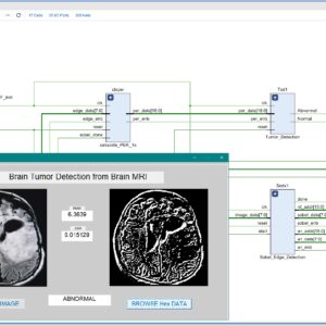
FPGA-Based Brain Tumor Detection from MRI Using 3×3 Convolution Soft IP Core with Stride 1
Base Paper Abstract:
This paper presents an efficient FPGA-based system for automatic brain tumor detection from MRI images using a 3x3 convolutional edge detection method with stride 1. The proposed architecture is developed as a soft IP core in Verilog HDL and synthesized on a Xilinx Zynq 7000 FPGA platform. The system applies a customized 3x3 convolution kernel over each MRI image with stride 1, ensuring that every pixel is processed and fine image details are preserved for accurate tumor detection. Edge detection results are used to segment and highlight abnormal regions, and a thresholding mechanism is employed to differentiate between normal and abnormal images. Hardware resource utilization—including look-up tables (LUTs), flip-flops (FFs), and power consumption—is analyzed after synthesis to verify system efficiency. Experimental results confirm that the proposed FPGA implementation provides real-time processing and reliable brain tumor detection with low power usage, making it suitable for portable and embedded medical devices. The stride 1 approach guarantees maximum detection accuracy and detailed edge representation in all test cases.
List of the following materials will be included with the Downloaded Backup:
Full-Array Boolean Logic CIM Macro with Self-Recycling 10T-SRAM Cell for AES Systems
Base Paper Abstract:
Computing in memory (CIM), which alleviates the need to transfer a large amount of data between processor and memory, significantly reducing latency and energy consumption, is a promising new computing architecture for addressing the von Neumann bottleneck problem. This article proposes a CIM array structure composed of self-recycling 10T static random access memory (SRAM) cells, which can realize orthogonal data writing, and multiple Boolean logical operations for the entire array. The self-recycling and full-array activation characteristics are extremely suitable for accelerating diverse data processing algorithms such as the Advanced Encryption Standard (AES). A 4-kb SRAM is implemented in 55-nm CMOS technology to verify the effectiveness of the design. Compared with other state-of-threat architectures, the throughput and the operating frequency of the proposed CIM macro are increased to 843 GOPS/kb (2.64×) and 823.7 MHz (2.6×), respectively. The energy efficiency reaches 246.9 TOPS/W. When applied to the AES, the energy consumption is 35.77% less than the digital CIM architecture that is not self-recycling.
List of the following materials will be included with the Downloaded Backup:
Hardware Implementation of Improved Banker’s Fixed-Point Rounding Algorithm
Base Paper Abstract:
In recent years, FPGA-based convolutional neural networks (CNNs) accelerator has received tremendous research interest, especially in fields such as autonomous driving and robotics. For the purpose of accelerating convolution computations, Winograd fast convolution algorithm is frequently employed. However, during implementation of the Winograd algorithm on FPGA, multiple rounding operations occur, and the accuracy of these operations substantially impacts the convolution results. The banker’s rounding algorithm, compared to other rounding algorithms, has advantages such as a more symmetric error distribution and smaller errors, making it suitable for Winograd convolution computation. However, the conventional banker’s rounding algorithm is proposed for floating-point calculations, yet FPGA implements fixed-point arithmetic. Moreover, it frequently rounds 0.5 to 0, leading to the issue of convolution weight invalidation and introducing significant errors. To overcome these challenges, an improved hardware circuit designed for implementing the fixed-point banker’s rounding algorithm is proposed. Experimental results show that compared with common rounding up and rounding down methods, the proposed algorithm exhibits smaller errors and effectively resolves the issue of weight invalidation in conventional banker’s rounding, leading to a significant 55.6% improvement in computational accuracy.
List of the following materials will be included with the Downloaded Backup:
High-performance CORDIC-based approximate MAC architectures for FPGA platforms
CORDIC is a versatile algorithm frequently used in different signal-processing operations. While using CORDIC based computations in evaluating trigonometric and transcendental functions is quite prevalent, the resource overhead associated with its implementation does not justify its use in evaluating linear functions like multiplication and addition. However, with the emergence of approximate computing as an attractive paradigm for error-resilient applications, the algorithm can be used to design approximate linear computational units that completely justify the accuracy-performance trade-offs. In this paper, we model the CORDIC-based computations to emulate the multiply-accumulate operation, albeit with some loss of accuracy. We specifically present two incremental CORDIC-based multiply-accumulate architectures with an attempt to improve the accuracy performance trade-offs with each increment. A detailed Pareto analysis for 8and16-bit unsigned and signed multiply-accumulate structures is conducted to determine the optimum number of computing stages and the associated bit-precision of the intermediate results. Accuracy and performance analysis using 6th and 7th generation FPGA reveals a substantial improvement overstate-of-the-art designs. The proposed architectures are also tested using three image processing applications, and the output results are promising.
List of the following materials will be included with the Downloaded Backup:
Hybrid Approximate Multipliers with Merits Balance for Digital Processing and Neural Networks
In this article, hybrid approximate multiplier (HAMs) designs based on the combination of logarithmic multiplication and piecewise linear (PWL) fitting are proposed. After extracting the exponent and mantissa of the input operands, two new variables are introduced to perform spatial mixed linear fitting on the 3-D surface of the mantissa product in different regions. Limited power-of-2 elements in line slopes make the multivariable mixed PWL computational simple and friendly to logic circuit complexity. With iterative adjustment of the slopes and bias of the lines in the PWL calculation, the relative error distance (RED) distribution is well balanced and zero concentrated. In addition, we detail the logic architecture to implement approximate hybrid accumulation and error tolerant complement conversions. In the 45-nm library-based performance comparison, the proposed multipliers mainly 16-, 8-, and 32-bit floating-point multipliers exhibit >55% power, >23% delay, and >43% area reductions compared with the exact multiplier. In addition, they outperform other state-of-the-art designs in terms of delay, power, area, and error, as evaluated by the joint delay–power–area product (PPA) and mean RED (MRED). In case experiments, the proposed multipliers perform nearly equivalently to the exact multiplier in error-tolerant digital processing and neural network computations. Index Terms Approximate multiplier, arithmetic digital circuit, computational logic architecture, logarithmic multiplier, piecewise linear (PWL).
List of the following materials will be included with the Downloaded Backup:
Lightweight, High-Entropy TRNG Using Quad Cross-Coupled Feedback Architecture
Base Paper Abstract:
This paper presents a lightweight, high-entropy true random number generator architecture featuring an innovative quad cross-coupled feedback mechanism to enhance randomness. The primary goal is to develop an efficient and secure true random number generator that addresses the growing demand for reliable random number generation in cryptographic and security-critical applications. The motivation stems from the need to improve entropy, reduce resource utilization, and ensure robustness across varying technologies. With the intention of achieving near-perfect randomness, the Quad-Input Oscillating Circuit module integrates self-coupled, jitter-inducing ring oscillators with cross-coupled feedback loops to induce metastability. Comprehensive evaluations confirm a Shannon entropy of 0.999818, a minimum entropy of 0.977257, and a collision entropy of 0.999636. The design was synthesized using Synopsys Design Compiler at 45 nm, 32 nm, and 14 nm, achieving a maximum frequency of 6.7 GHz, power consumption as low as 72 μW, and area utilization of 24 μm2 at 14 nm. Rigorous validation through multiple statistical test suites, including the AIS-31, Autocorrelation, Deviation, Diehard, the National Institute of Standards and Technologies SP800- 22 and SP800-90B, and TestU01, confirms its efficiency and reliability. Real random bits were implemented as oscilloscope viewable signals on the Cyclone V Field Programmable Gate Array developed by Altera, representing a significant advancement in secure random number generation technologies.
List of the following materials will be included with the Downloaded Backup:
Low-Complexity Implementation of Real-Time Reconfigurable Low-Pass Equalizers
Implementation techniques and results for a recently proposed real-time reconfigurable low-pass equalizer (RLPE) consisting of a variable bandwidth (VBW) filter and a variable equalizer (VE) are presented. Both components utilize fixed finite-length impulse response (FIR) filters combined with a few general multipliers, resulting in lower area and power consumption compared to a general FIR filter, despite requiring more multiplications. This is because the constant multipliers in the fixed FIR filters of the RLPE can be optimized for implementation. An additional advantage is that the proposed RLPE does not require online design. Various implementation alternatives for fixed FIR filters, including ways to increase the frequency, are evaluated to optimize the implementation of the RLPE. Several versions of the proposed RLPE and a general FIR filter for comparison are implemented using a 28-nm fully depleted silicon on insulator (FD-SOI) standard cell library. The results demonstrate that the RLPE baseline design requires less power and area than the general equalizer, and although the frequency of the baseline implementation is lower, the design can reach the same frequency while still having significantly less power and area. Furthermore, an approach is introduced to break the chain in the polynomial section of the VBW filter by using fewer additional registers compared to standard pipelining. Instead, this method reformulates the constant multiplication problem to produce correct results. For the considered case, the power consumption is reduced between 49% and 70% for different frequencies, with an area decrease in the range of 64% to 67%, by using the proposed RLPE compared to a general FIR filter. Index Terms: Constant multiplications, real-time reconfiguration, variable bandwidth (VBW) low-pass filter, variable equalizer (VE).
List of the following materials will be included with the Downloaded Backup:
Low-Power and High-Speed SRAM Cells With Double-Node Upset Self-Recovery for Reliable Applications
Transistor sizing and spacing are constantly decreasing due to the continuous advancement of CMOS technology. The charge of the sensitive nodes in the static random access memory (SRAM) cell gradually decreases, making the SRAM cell more and more sensitive to soft errors, such as single node upsets (SNUs) and double node upsets (DNUs). Therefore, two types of radiation-hardened SRAM cells are proposed in this article. First, a low-power DNU self-recovery S6P8N cell is proposed. This cell can realize SNU self-recovery from all sensitive nodes as well as realize partial DNUs self-recovery and has low-power consumption overhead. Second, we propose a high-speed DNU self-recovery S8P6N cell, which has a soft-error tolerance level similar to the S6P8N. Furthermore, it reduces the read access time (RAT) and write access time (WAT). Simulation results show that the proposed cells are self-recovery for all SNUs and most of DNUs. Compared with RHD12, QCCM12T, QUCCE12T, RHMD10T, SEA14T, RHM-12T, S4P8N, S8P4N, RH-14T, HRLP16T, CC18T, and RHM, the average power consumption of S6P8N is reduced by 48.78%, and the average WAT is reduced by 6.62%. While the average power consumption of S8P6N is reduced by 23.64%, and the average WAT and RAT by 9.07% and 36.84%, respectively. Index Terms: Double-node upsets (DNUs), high-speed, low power, self-recovery, static random access memory (SRAM).
List of the following materials will be included with the Downloaded Backup:
Low-Power High Precision Floating-Point Divider with Bidimensional Linear Approximation
Base Paper Abstract:
In this paper we propose a novel approximate floating-point divider based on bi-dimensional linear approximation. In our approach, the mantissa quotient is seen as a function of the two input mantissas of the divider. The domain of this two-variable function is partitioned into nx × ny subregions, named tiles, where nx, ny are chosen as powers of two. In each tile the quotient is approximated with a linear combination of the input mantissas. To achieve fine accuracy, an optimization problem is formulated within each tile to determine the optimal coefficients for the linear combination, which minimize the Mean Relative Error Distance (MRED) of the divider. Furthermore, to make hardware implementation more effective, the minimization problem is appropriately modified to search for optimal quantized coefficients. The hardware structure of the divider only requires a small look-up table to store the linear approximation coefficients, and a carry save adder tree. The proposed architecture is highly tunable at design-time over a wide range of accuracy, depending on the number of tiles chosen for the approximation. The obtained results demonstrate error performance and hardware features superior to the state-of-the-art. The proposed dividers define the Pareto front, considering the trade-off between power-delay-product vs. MRED and area-delay-product vs. MRED, for MRED in the range of 4 × 10⁻³ − 2 × 10⁻². Application results for JPEG compression and tone mapping further highlight the strength of our proposal, which exhibits Structural Similarity Index (SSIM) very close to 1 in all cases and Peak Signal-to-Noise Ratio (PSNR) up to 45 db. Index Terms: Floating-point divider, approximate computing, error correction, low-power.
List of the following materials will be included with the Downloaded Backup:
Low-Power, Low-Energy, Static, Contention-Free, TSPC Dual-Edge Triggered Flip-Flops
Base Paper Abstract:
The dual edge-triggered flip-flop samples the data on both the positive and negative edges of the clock. Hence, it can lead to lower clock relative power consumption as compared to the single-edge triggered flip-flop while maintaining the same data throughput. In this paper, we present two low-power, low-energy dual-edge triggered TSPC flip-flops based on latch-mux type methodology. These two flip-flops, Low-Power at Low Data Activity (LPLD-DET), and Low-Power at High Data Activity (LPHD-DET) are suitable for low-power application. These flip-flops are fully static and contention-free. The post-layout simulation results in TSMC CMOS 65 nm technology suggest that the proposed LPLD-DET is the most power-efficient dual-edge triggered flip-flop for low data activities up to 30%, and LPHD-DET is the most power-efficient dual-edge triggered flip-flop for higher data activities from 45% compared to the other state of-the-art dual-edge triggered TSPC flip-flops.
List of the following materials will be included with the Downloaded Backup:
Resource and Energy Efficient Implementation of ECG Classifier using Binarized CNN for Edge AI Devices
Base Paper Abstract:
Wearable Artificial Intelligence-of-Things (AIoT) devices demand smart gadgets that are both resource and energy-efficient. In this paper, we explore efficient implementation of binary convolutional neural network employing function merging and block reuse techniques. The hardware implemented in field programmable gate array (FPGA) platform can classify ventricular beat in electrocardiogram achieving accuracy of 97.5%, sensitivity of 85.7%, specificity of 99.0%, precision of 92.3%, and F1-score of 88.9% while consuming only 10.5-µW of dynamic power dissipation.
List of the following materials will be included with the Downloaded Backup:
Scalable JTAG-Based 32-Bit Memory Test Architecture with MATS+ and MATS++/March-C Fault Detection
Proposed Abstract:
Embedded memories are increasingly used in advanced System-on-Chip (SoC) designs for applications such as networking, automotive control, and medical imaging, where reliability and performance are critical. Ensuring fault-free operation of these memories is essential, yet memory testing remains a major challenge. Conventional MBIST architectures, while effective, often introduce significant silicon overhead, add design complexity, and lack flexibility for post-fabrication updates. In addition, existing memory test algorithms have their own drawbacks: March-C is widely applied and provides high fault coverage, but it requires long test times due to bit-oriented operations and large numbers of read–write cycles; MATS+ is simple and efficient but suffers from lower coverage, particularly for coupling and complex dynamic faults; and MATS++ improves on MATS+ with better detection capability, yet it still trades off hardware cost and scalability when applied to larger 32-bit word-oriented memories. Furthermore, most existing implementations are optimized for small SRAMs and are not easily scalable to clustered embedded memories in SoCs, nor do they fully exploit standard boundary-scan infrastructure for low-cost testing. To address these problems, this work proposes a scalable JTAG-based 32-bit memory test architecture that reuses IEEE 1149.1 boundary-scan resources to apply and compare March-C, MATS+, and MATS++ algorithms in both single-bit and multi-bit test modes. The proposed framework minimizes additional hardware cost by integrating BIST control into boundary-scan registers, while enabling algorithm programmability and flexibility for different memory clusters. The novelty lies in providing a detailed performance comparison of these algorithms under a unified boundary-scan-based architecture, focusing on trade-offs between fault coverage, test time, and silicon overhead. The design is implemented in Verilog HDL and synthesized on an FPGA using Xilinx Vivado, where parameters such as area, power, and latency are evaluated to validate efficiency and practical applicability for SoC-level memory testing.
List of the following materials will be included with the Downloaded Backup:Provide Wordlwide Online Support
We can provide Online Support Wordlwide, with proper execution, explanation and additionally provide explanation video file for execution and explanations.
24/7 Support Center
NXFEE, will Provide on 24x7 Online Support, You can call or text at +91 9789443203, or email us nxfee.innovation@gmail.com
Terms & Conditions:
Customer are advice to watch the project video file output, and before the payment to test the requirement, correction will be applicable.
After payment, if any correction in the Project is accepted, but requirement changes is applicable with updated charges based upon the requirement.
After payment the student having doubts, correction, software error, hardware errors, coding doubts are accepted.
Online support will not be given more than 3 times.
On first time explanation we can provide completely with video file support, other 2 we can provide doubt clarifications only.
If any Issue on Software license / System Error we can support and rectify that within end of day.
Extra Charges For duplicate bill copy. Bill must be paid in full, No part payment will be accepted.
After payment, to must send the payment receipt to our email id.
Powered by NXFEE INNOVATION, Pondicherry.
Call us today at : +91 9789443203 or Email us at nxfee.innovation@gmail.com
NXFEE Development & Services

Product Categories
- 2014 (11)
- 2015 (39)
- 2016 (30)
- 2017 (16)
- 2018 (17)
- 2019 (42)
- 2020 (29)
- 2021 (17)
- 2022 (23)
- Accessories (39)
- Area Efficient (115)
- High speed VLSI Design (56)
- IEEE (15)
- Image Processing (39)
- Low power VLSI Design (94)
- NOC VLSI Design (2)
- VLSI (244)
- VLSI 2023 (21)
- VLSI 2024 (16)
- VLSI 2025 (28)
- VLSI 2026 (2)
- VLSI Application / Interface and Mini Projects (30)
- VLSI_2023 (15)
Filter by price
Product Status
Sort by producents

Copyright © 2026 Nxfee Innovation.