Improvements:
- To develop the two stage CMOS Operational trans conductance Amplifier using 45nm and 22nm CMOS technology and comparing in terms of power, gain and supply voltage.
- To implement the OTA in order to enhance intrinsic gain with the minimal power consumption of advanced 22nm and 45nm CMOS technology.
Proposed abstract:
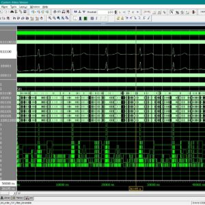
Operational trans conductance amplifiers (OTAs) are widely used in sensor interfaces, biomedical circuits, switched-capacitor systems, data converters, and low-power communication blocks because they offer high linearity, tuneable trans conductance, and compatibility with advanced CMOS processes. While modern technology nodes provide advantages such as reduced chip area, higher intrinsic speed, and lower supply voltages, they also introduce disadvantages including reduced intrinsic gain, increased leakage, and tighter design margins. These challenges motivate the need for improved amplifier architectures capable of maintaining high gain and low power consumption in deeply scaled CMOS. Existing OTAs in advanced nodes typically rely on cascading, gain boosting, or multi-stage compensation, but these methods increase circuit complexity and power, and often lose efficiency at low supply voltages. To address these issues, this work proposes the design and comparative analysis of a two-stage CMOS OTA implemented in 45-nm and 22-nm technology nodes, targeting enhanced intrinsic gain with minimal power consumption. The approach focuses on optimized transistor sizing, low-voltage bias strategies, and compensation techniques inspired by recent advancements in stable two-stage amplifiers, such as zero-tracking and improved Miller compensation, as observed in recent literature and device behaviour trends. The novelty of this work lies in demonstrating how advanced-node short-channel effects can be exploited rather than mitigated, using device parameters to enhance gain while preserving low-power operation across both technology options. Performance metrics including dc gain, unity-gain bandwidth, phase margin, output swing, offset, and total power consumption are evaluated through Cadence Virtuoso and Spectre simulations, with additional verification using MATLAB-based analytical models for consistency across scenarios.
Software Implementation:
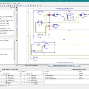
- Tanner EDA
” Thanks for Visit this project Pages – Buy It Soon “
A Low-Power Two-Stage CMOS OTA in 22 nm and 45 nm Technologies with Enhanced Gain and Power Efficiency
Terms & Conditions:
- Customer are advice to watch the project video file output, before the payment to test the requirement, correction will be applicable.
- After payment, if any correction in the Project is accepted, but requirement changes is applicable with updated charges based upon the requirement.
- After payment the student having doubts, correction, software error, hardware errors, coding doubts are accepted.
- Online support will not be given more than 3 times.
- On first time explanations we can provide completely with video file support, other 2 we can provide doubt clarifications only.
- If any Issue on Software license / System Error we can support and rectify that within end of the day.
- Extra Charges For duplicate bill copy. Bill must be paid in full, No part payment will be accepted.
- After payment, to must send the payment receipt to our email id.
- Powered by NXFEE INNOVATION, Pondicherry.
Payment Method :
- Pay Add to Cart Method on this Page
- Deposit Cash/Cheque on our a/c.
- Pay Google Pay/Phone Pay : +91 9789443203
- Send Cheque through courier
- Visit our office directly
- Pay using Paypal : Click here to get NXFEE-PayPal link
Bank Accounts
HDFC BANK ACCOUNT:
- NXFEE INNOVATION,
HDFC BANK, MAIN BRANCH, PONDICHERRY-605004.
INDIA,
ACC NO. 50200090465140,
IFSC CODE: HDFC0000407.