Improvements:
- To design RHD12, QCCM12T, QUCCE12T, RHMD10T, SEA14T, RHM-12T, S4P8N, S8P4N, RH-14T, HRLP16T, CC18T, and RHM cell using 22 nm CMOS technology and comparing in terms of delay, area and power consumption.
- To design and develop S6P8N and S8P6N cell of SRAM using 22nm CMOS technology.
Proposed abstract:
Static random-access memory (SRAM) is widely used in aerospace, defence, medical electronics, and other radiation-prone applications because of its high speed, low latency, and low operating voltage. However, as device dimensions’ shrink in advanced CMOS technologies, conventional SRAM cells become increasingly sensitive to radiation-induced soft errors, offering advantages in density and speed but suffering from disadvantages such as reduced node charge, higher upset probability, and limited self-recovery capability. Existing radiation-hardened SRAM cells, including RHD12, QCCM12T, QUCCE12T, RHMD10T, SEA14T, RHM-12T, S4P8N, S8P4N, RH-14T, HRLP16T, CC18T, and RHM, provide improved protection from single-node and double-node upsets but still show drawbacks such as higher power consumption, larger delay, or limited recovery of DNU pairs. To address these challenges, this work designs and compares all these hardened cells using 22 nm CMOS technology, identifying their strengths and limitations in terms of delay, power, and area. Building on these findings, two new SRAM architectures, S6P8N and S8P6N, are designed to enhance soft-error tolerance without adding structural complexity. The proposed cells use optimized transistor placement and redundancy to achieve full recovery from all single-node upsets and 67% recovery of double-node upset cases, while also reducing average power in S6P8N and improving read and write speed in S8P6N. The novelty of this work lies in achieving a balanced improvement in reliability, speed, and power efficiency compared to existing state-of-the-art hardened designs. All SRAM cells, including the proposed ones, are developed, simulated, and evaluated using Tanner EDA tools under 22 nm CMOS technology files. Performance is analysed through power, delay, area, read access time, write access time, static noise margin, and Monte-Carlo simulation results, confirming that the proposed S6P8N and S8P6N architectures offer a strong and scalable solution for next-generation radiation-tolerant memory systems.
Software Implementation:
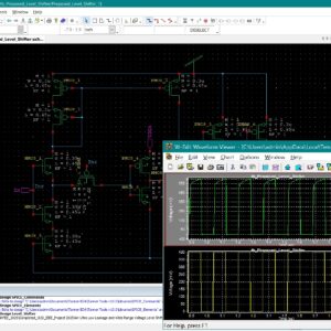
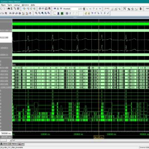
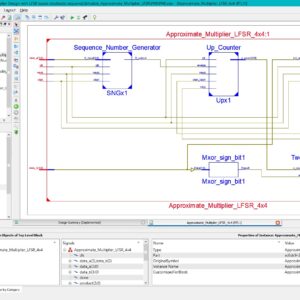
- Tanner EDA
” Thanks for Visit this project Pages – Buy It Soon “
Radiation-Tolerant SRAM Design with Enhanced Self-Recovery Using S6P8N and S8P6N Architectures in 22 nm CMOS Technology
Terms & Conditions:
- Customer are advice to watch the project video file output, before the payment to test the requirement, correction will be applicable.
- After payment, if any correction in the Project is accepted, but requirement changes is applicable with updated charges based upon the requirement.
- After payment the student having doubts, correction, software error, hardware errors, coding doubts are accepted.
- Online support will not be given more than 3 times.
- On first time explanations we can provide completely with video file support, other 2 we can provide doubt clarifications only.
- If any Issue on Software license / System Error we can support and rectify that within end of the day.
- Extra Charges For duplicate bill copy. Bill must be paid in full, No part payment will be accepted.
- After payment, to must send the payment receipt to our email id.
- Powered by NXFEE INNOVATION, Pondicherry.
Payment Method :
- Pay Add to Cart Method on this Page
- Deposit Cash/Cheque on our a/c.
- Pay Google Pay/Phone Pay : +91 9789443203
- Send Cheque through courier
- Visit our office directly
- Pay using Paypal : Click here to get NXFEE-PayPal link
Bank Accounts
HDFC BANK ACCOUNT:
- NXFEE INNOVATION,
HDFC BANK, MAIN BRANCH, PONDICHERRY-605004.
INDIA,
ACC NO. 50200090465140,
IFSC CODE: HDFC0000407.