₹10,000.00Original price was: ₹10,000.00.₹6,000.00Current price is: ₹6,000.00.
Source : Tanner EDABase paper abstract:
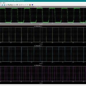
This brief presents a 55-nm level shifter (LS) that enables wide voltage range conversion from 80 mV to 1.2 V with high energy efficiency and fast transition speed. The proposed design incorporates a complementary output buffer and an assist discharge path to suppress the short-circuit current and enhance the transition speed. A multi threshold transistor strategy is adopted to expand the input range and reduce static power. Measurement results across 15 samples demonstrate robust subthreshold performance with 4.4-ns transition delay and 49.1-fJ/transition energy during 0.3–1.2-V conversion at 1 MHz. The measured average minimum convertible input voltages are 80 and 139 mV at input frequencies of 50 kHz and 1 MHz, respectively. The compact layout occupies only 7.96 µm 2. Compared to the best benchmarked prior work, the proposed LS achieves 33.8% improvement in energy-delay metrics, making it a highly efficient and scalable solution for energy constrained systems and the Internet of Things (IoT). Index Terms: Current mirror (CM), dual supply, level shifter (LS), low power, subthreshold.
List of the following materials will be included with the Downloaded Backup:
₹10,000.00Original price was: ₹10,000.00.₹6,000.00Current price is: ₹6,000.00.
Source : Tanner EDA
Abstract:
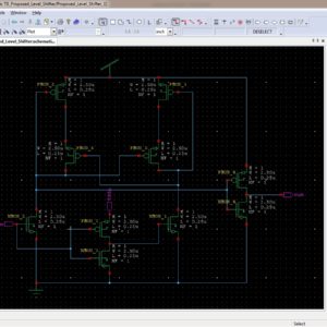
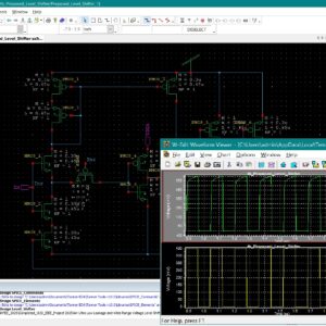
In this brief, a fast and very low power voltage level shifter (LS) is presented. By using a new regulated cross-coupled (RCC) pull-up network, the switching speed is boosted and the dynamic power consumption is highly reduced. The proposed (LS) has the ability to convert input signals with voltage levels much lower than the threshold voltage of a MOS device to higher nominal supply voltage levels. The presented LS occupies a small silicon area owing to its very low number of elements and is ultra-low-power, making it suitable for low-power applications such as implantable medical devices and wireless sensor networks. Results of the post-layout simulation in a standard 0.18-μm CMOS technology show that the proposed circuit can convert up input voltage levels as low as 80 mV. The power dissipation and propagation delay of the proposed level shifter for a low/high supply voltages of 0.4/1.8 V and input frequency of 1 MHz are 123.1 nW and 23.7 ns, respectively.
List of the following materials will be included with the Downloaded Backup:
₹12,000.00Original price was: ₹12,000.00.₹6,000.00Current price is: ₹6,000.00.
Source : Tanner EDA
Base Paper Abstract:
This brief presents an ultra-low leakage and fast conversion level shifter with wide-range voltage conversion and frequency. The proposed level shifter adopts the leakage shutoff transistors, which can completely cut off the static current when the circuits stand by. The pull-down network employs the low-threshold transistor for the fast fall transition. The proposed level shifter also solves the swing problem and achieves a fast conversion by using the voltage hysteresis transistor, strengthening the pull-up network to ensure the internal node is fast and fully charged. Measurement results based on the 55 nm process show that the average ultra-low leakage of the proposed level shifter is 34.8 pW when converting from 0.3 V input to 1.2 V output. Meanwhile, the average propagation delay and the average energy per transition of the proposed level shifter are 13.86 ns and 22.71 fJ for an input frequency of 1 MHz, respectively. The maximum conversion range is from 0.13 V to 1.2 V. Index Terms: Level shifter, ultra-low power, multi-supply voltage circuit, sub-threshold operation.
List of the following materials will be included with the Downloaded Backup:
₹10,000.00Original price was: ₹10,000.00.₹6,000.00Current price is: ₹6,000.00.
Source : TANNER EDA
Abstract:
An instantaneous power consuming level shifter is presented in this paper to increase the DC converter efficiency. The level shifter is used in a high-side power switch driver to remove the external capacitor which is used in bootstrap technique. The level shifter consumes power only during the transition period. A delay cell is used to turn the level shifter off to reduce the power consumption period. An output voltage detector is added to turn the level shifter off even before the delay time. An asynchronous discontinuous conduction mode buck converter is designed to verify the performance of the level shifter. Simulation results show that the power consumption of the proposed level shifter decreased by 66%, while the converter efficiency increased by the maximum of 9% compared to results obtained for a conventional level shifter. The converter is fabricated using the TSMC 0.18-µm BCD process and it operates within an input range of 2–5 V when the current varies from 400 µA to 18 mA and delivers an output voltage of 1.8 V.
List of the following materials will be included with the Downloaded Backup:
We can provide Online Support Wordlwide, with proper execution, explanation and additionally provide explanation video file for execution and explanations.
24/7 Support Center
NXFEE, will Provide on 24x7 Online Support, You can call or text at +91 9789443203, or email us nxfee.innovation@gmail.com
Terms & Conditions:
Customer are advice to watch the project video file output, and before the payment to test the requirement, correction will be applicable.
After payment, if any correction in the Project is accepted, but requirement changes is applicable with updated charges based upon the requirement.
After payment the student having doubts, correction, software error, hardware errors, coding doubts are accepted.
Online support will not be given more than 3 times.
On first time explanation we can provide completely with video file support, other 2 we can provide doubt clarifications only.
If any Issue on Software license / System Error we can support and rectify that within end of day.
Extra Charges For duplicate bill copy. Bill must be paid in full, No part payment will be accepted.
After payment, to must send the payment receipt to our email id.
Powered by NXFEE INNOVATION, Pondicherry.
Call us today at : +91 9789443203 or Email us at nxfee.innovation@gmail.com