₹12,000.00Original price was: ₹12,000.00.₹6,000.00Current price is: ₹6,000.00.
Source : Tanner EDA
Abstract:
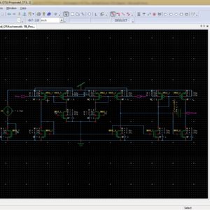
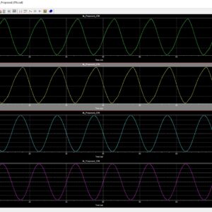
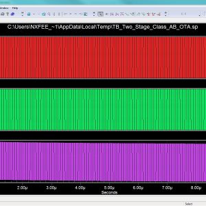
In this article, a new solution for an ultralow-voltage (ULV) ultralow-power (ULP) operational transconductance amplifier (OTA) is presented. Thanks to the combination of a low-voltage bulk-driven nontailed differential stage with the multipath Miller zero compensation technique, a simple class AB power-efficient ULV structure has been obtained, which can operate from supply voltages less than the threshold voltages of the employed MOS transistors, while offering rail-to-rail input common-mode range at the same time. The proposed OTA was fabricated using the 180-nm CMOS process from Taiwan Semiconductor Manufacturing Company (TSMC) and can operate from VDD ranging from 0.3 to 0.5 V. The 0.3-V version dissipates only 12.6 nW of power while showing a 64.7-dB voltage gain at 1-Hz, 2.96-kHz gain-bandwidth product, and a 4.15-V/ms average slew-rate at 30-pF load capacitance. The measured results agree well with simulations.
List of the following materials will be included with the Downloaded Backup:
₹10,000.00Original price was: ₹10,000.00.₹6,000.00Current price is: ₹6,000.00.
Source : Tanner EDA
Base Paper Abstract:
This brief implements a highly efficient fully differential trans conductance amplifier, based on several input-to-output paths. Some traditional techniques, such as positive feedback, nonlinear tail current sources, and current mirror-based paths, are combined to increase the trans conductance, thus leading to larger dc gain and higher gain bandwidth (GBW) product. Two flipped voltage-follower (FVF) cells are employed as variable current sources to provide class-AB operation and adaptive biasing of all other drivers. The proposed structure includes several input-to-output paths that play the role of dynamic current boosters during the slewing phase, thus improving the slew rate (SR) performance. The circuit was fabricated in a TSMC 0.18-µm CMOS process with a silicon area of 54.5 × 30.1 µm. Experimental results show a GBW of 173.3 MHz, a dc gain of 72.7 dB, and an SR of 139.4 V/µs for a capacitive load of 2 × 5 pF. The proposed circuit consumes 619 µW of power, under a supply voltage of 1.8 V.
List of the following materials will be included with the Downloaded Backup:
₹15,000.00Original price was: ₹15,000.00.₹6,000.00Current price is: ₹6,000.00.
Source Code : TANNERAbstract:
In this paper, a new design procedure has been proposed for realization of logarithmic function via three phases: 1) differentiation; 2) division; and 3) integration for any arbitrary analog signal. All the basic building blocks, i.e., differentiator, divider, and integrator, are realized by operational transconductance amplifier, a current mode device. Realization of exponential, power law and hyperbolic function as the design examples claims that the proposed synthesis procedure has the potential to design a log-based nonlinear system in a systematic and hierarchical manner. The proposed architecture of this paper area and power consumption analysis using tanner tool.
List of the following materials will be included with the Downloaded Backup:
₹16,000.00Original price was: ₹16,000.00.₹10,000.00Current price is: ₹10,000.00.
Source : Verilog HDL
Abstract:
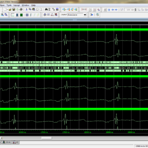
Electrocardiogram (ECG) is a form of cardiovascular measurement, for the diagnosis of different heart rate conditions. However, numerous noises usually harm the amplitude and time period of the signal from the ECG signal, at following a transition of the analog ECG signal from the sensor module into a digital format. The appropriate digital filter may be used to remove different forms of noise such as Baseline Wander, Power line interference, High frequency noise and Physiological Artifacts. The Digital FIR filter will have prospected to reduced the artifacts in the ECG signals. The signals taken from the MIT-BIH data base which contains the normal and abnormal waveforms. This Digital FIR filter can have more performance by using more TAP numbers such as multiplying, delaying and getting more effectiveness. This proposed work would implement a 1 norm minimization in the FIR filter with liner step method to minimize sparse complexity and reduce the mini-max approximation error for sparse maximization. Given these facts, several rules for selecting indicators of potential zero coefficients to be used in 1 standard optimization are adopted in the proposed algorithm. The efficacy of the proposed design algorithm was developed in Verilog HDL, simulated in Modelsim software and synthesized in Xilinx vertex 5 FPGA, and finally prove all the parameters in terms of area, delay and power.
List of the following materials will be included with the Downloaded Backup:
₹10,000.00Original price was: ₹10,000.00.₹6,000.00Current price is: ₹6,000.00.
Source : Tanner EDA
Base Paper Abstract:
An approach for the design of two-stage class AB OTAs with sub-1µA current consumption is proposed and demonstrated. The approach employs MOS transistors operating in subthreshold and allows maximum gain-bandwidth product (GBW) to be achieved for a given DC current budget, by setting optimum distribution of DC currents in the two amplifier stages. Following this strategy, a class AB OTA was designed in a standard 0.5-µm CMOS technology supplied from 1.6-V and experimentally tested. Measured GBW was 307 kHz with 980-nA DC current consumption while driving an output capacitance of 40 pF with an average slew rate of 96 V/ms.
List of the following materials will be included with the Downloaded Backup:
We can provide Online Support Wordlwide, with proper execution, explanation and additionally provide explanation video file for execution and explanations.
24/7 Support Center
NXFEE, will Provide on 24x7 Online Support, You can call or text at +91 9789443203, or email us nxfee.innovation@gmail.com
Terms & Conditions:
Customer are advice to watch the project video file output, and before the payment to test the requirement, correction will be applicable.
After payment, if any correction in the Project is accepted, but requirement changes is applicable with updated charges based upon the requirement.
After payment the student having doubts, correction, software error, hardware errors, coding doubts are accepted.
Online support will not be given more than 3 times.
On first time explanation we can provide completely with video file support, other 2 we can provide doubt clarifications only.
If any Issue on Software license / System Error we can support and rectify that within end of day.
Extra Charges For duplicate bill copy. Bill must be paid in full, No part payment will be accepted.
After payment, to must send the payment receipt to our email id.
Powered by NXFEE INNOVATION, Pondicherry.
Call us today at : +91 9789443203 or Email us at nxfee.innovation@gmail.com