₹10,000.00Original price was: ₹10,000.00.₹7,000.00Current price is: ₹7,000.00.
Source Code : TANNERAbstract:
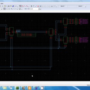
This paper explores the use of transformer-coupled (TC) technique for the 2:1 MUX and the 1:2 DEMUX to serialize-and-deserialize (SerDes) high-speed data sequence. The widely used current-mode logic (CML) designs of latch and multiplexer/demultiplexer (MUX/DEMUX) are replaced by the proposed TC approach to allow the more headroom and to lower the power consumption. Through the stacked transformer, the input clock pulls down the differential source voltage of the TC latch and the TC multiplexer core while alternating between the two-phase operations. With the enhanced drain-source voltage, the TC design attracts more drain current with less width-to-length ratio of NMOS than that of the CML counterpart. The source-offset voltage is decreased so that the supply voltage can be reduced. The lower supply voltage improves the power consumption and facilitates the integration with low voltage supply SerDes interface. The MUX and the DEMUX chips are fabricated in 65-nm standard CMOS process and operate at 0.7-V supply voltage. The chips are measured up to 40-Gb/s with sub-hundred milliwatts power consumption.
List of the following materials will be included with the Downloaded Backup:
₹10,000.00Original price was: ₹10,000.00.₹7,000.00Current price is: ₹7,000.00.
Source Code : TANNERAbstract:
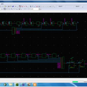
This paper presents a robust energy/area-efficient receiver fabricated in a 28-nm CMOS process. The receiver consists of eight data lanes plus one forwarded-clock lane supporting the hyper transport standard for high-density chip-to-chip links. The proposed all-digital clock and data recovery (ADCDR) circuit, which is well suited for today’s CMOS process scaling, enables the receiver to achieve low power and area consumption. The ADCDR can enter into open loop after lock-in to save power and avoid clock dithering phenomenon. Moreover, to compensate the open loop, a phase tracking procedure is proposed to enable the ADCDR to track the phase drift due to the voltage and temperature variations. Furthermore, the all-digital delay-locked loop circuit integrated in the ADCDR can generate accurate multiphase clocks with the proposed calibrated locking algorithm in the presence of process variations. The precise multiphase clocks are essential for the half-rate sampling and Alexander-type phase detecting. Measurement results show that the receiver can operate at a data rate of 6.4 Gbits/s with a bit error rate. The proposed architecture of this paper area and power consumption analysis using tanner tool.
List of the following materials will be included with the Downloaded Backup:
₹10,000.00Original price was: ₹10,000.00.₹7,500.00Current price is: ₹7,500.00.
Source Code : TANNERAbstract:
Ring oscillators (ROs) are popular due to their small area, modest power, wide tuning range, and ease of scaling with process technology. However, their use in many applications is limited due to poor phase noise and jitter performance. Thermal noise and flicker noise contribute jitter that decreases inversely with oscillation frequency. This paper describes a frequency boost technique to reduce jitter in ROs. We boost the internal oscillation frequency and introduce a frequency divider following the oscillator to maintain the desired output frequency. This approach offers reduced jitter as well as the opportunity to trade off output jitter with power for dynamic performance management. The oscillator has 32 operating modes, corresponding to different values for the ring size and frequency division. In a 0.5-µm CMOS process, the highest oscillation frequency achieved is 25 MHz with a root-mean-square period jitter of 54 ps and a power consumption of 817 µW at 5 V supply. A jitter model for current-starved oscillators was derived and verified by measurement; a direct relationship between oscillation frequency and jitter was derived and measured. Compared with other oscillators, this design achieves the highest performance in terms of jitter per unit interval and figure-of-merit. The performance is expected to improve in more advanced technologies. The results are summarized to offer design guidance based on the frequency boost technique. The proposed architecture of this paper area and power consumption analysis using tanner tool.
List of the following materials will be included with the Downloaded Backup:
We can provide Online Support Wordlwide, with proper execution, explanation and additionally provide explanation video file for execution and explanations.
24/7 Support Center
NXFEE, will Provide on 24x7 Online Support, You can call or text at +91 9789443203, or email us nxfee.innovation@gmail.com
Terms & Conditions:
Customer are advice to watch the project video file output, and before the payment to test the requirement, correction will be applicable.
After payment, if any correction in the Project is accepted, but requirement changes is applicable with updated charges based upon the requirement.
After payment the student having doubts, correction, software error, hardware errors, coding doubts are accepted.
Online support will not be given more than 3 times.
On first time explanation we can provide completely with video file support, other 2 we can provide doubt clarifications only.
If any Issue on Software license / System Error we can support and rectify that within end of day.
Extra Charges For duplicate bill copy. Bill must be paid in full, No part payment will be accepted.
After payment, to must send the payment receipt to our email id.
Powered by NXFEE INNOVATION, Pondicherry.
Call us today at : +91 9789443203 or Email us at nxfee.innovation@gmail.com