
A Novel Quantum Dot Cellular Automata X bit × 32 bit SRAM
Original price was: ₹18,000.00.₹10,000.00Current price is: ₹10,000.00.
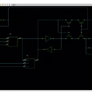
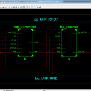
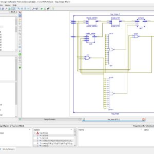
Source : VHDL
Abstract:
Application of quantum-dot cellular automata (QCA) technology as an alternative to CMOS technology on the nanoscale has a promising future; QCA is an interesting technology for building memory. The proposed design and simulation of a new memory cell structure based on QCA with a minimum delay, area, and complexity is presented to implement a static random access memory (SRAM). This paper presents the design and simulation of a 16-bit × 32-bit SRAM with a new structure in QCA. Since QCA is a pipeline, this SRAM has a high operating speed. The 16-bit × 32-bit SRAM has a new structure with a 32-bit width designed and implemented in QCA. It has the ability of a conventional logic SRAM that can provide read/write operations frequently with minimum delay. The 16-bit × 32-bit SRAM is generalized and an n × 16-bit × 32-bit SRAM is implemented in QCA. Novel 16-bit decoders and multiplexers (MUXs) in QCA are presented that have been designed with a minimum number of majority gates and cells. The new SRAM, decoders, and MUXs are designed, implemented, and simulated in QCA using a signal distribution network to avoid the coplanar problem of crossing wires. The QCA-based SRAM cell was compared with the SRAM cell based on CMOS. Results show that the proposed SRAM is more efficient in terms of area, complexity, clock frequency, latency, throughput, and power consumption.
List of the following materials will be included with the Downloaded Backup:
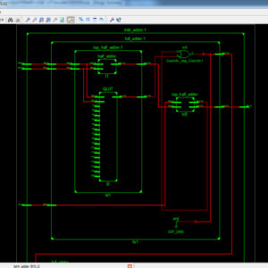
FPGA Implementation of Novel Quantum Dot Cellular Automata 256x 32 bit SRAM
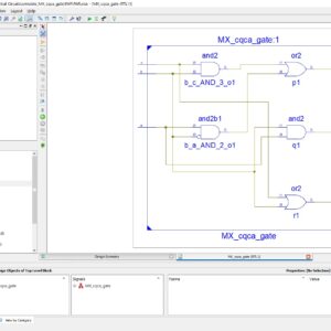
Proposed System:
- Increases the Bit size of 256×32, and reduced the Power
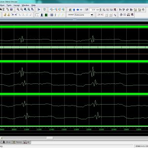
Advantages:
- Serial Read/Write Operation
- Multiple Bit Support
- Low Power Consumption
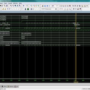
Software implementation:
- Modelsim
- Xilinx
Related products

 A Novel Quantum Dot Cellular A...
Original price was: ₹18,000.00.₹10,000.00Current price is: ₹10,000.00.
Reviews
There are no reviews yet.