
An Efficient VLSI Architecture of Reconfigurable VHBCSE based Pulse Shaping FIR Interpolation
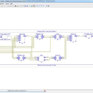
Proposed System:
- Use the VHBCSE algorithm for the multiplication process and Increases the Efficiency
Advantages:
- Area coverage is less
- Power consumption is less
Software implementation:
- Modelsim
- Xilinx


Reviews
There are no reviews yet.