Proposed System:
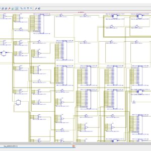
- Implemented 4:2, 5:2 and 7:2 compressor using same Adiabatic
Advantages:
- Reduce the power level
- Increases the efficiency
- Reduced the area size
Software implementation:
- DSCH3/Microwind
- Modelsim
- Xilinx
₹12,000.00 Original price was: ₹12,000.00.₹6,000.00Current price is: ₹6,000.00.
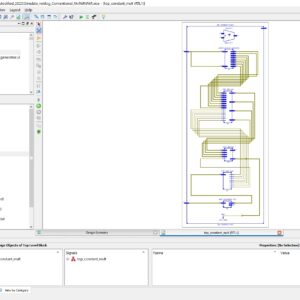
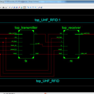
Source : VHDL & Verilog HDL ( DSCH3/MICROWIND)
Abstract:
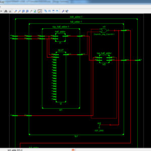
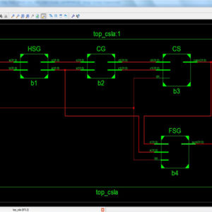
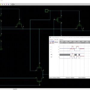
The Subthreshold adiabatic logic for Ultralow power application is a novel approach is efficient in low speed operations, where power consumption and longevity are the pivotal concerns instead of performance. Here, we are implementing the adiabatic logic gates and implementing CLA 8-bit, it will compared to the normal logic gates, the adiabatic logic makes a more power consumption and also increasing speed. The schematic and layout of a 4-bit carry look ahead adder (CLA) has been implemented to show the workability of the proposed logic. The effect of temperature and process parameter variations on sub threshold adiabatic logic-based 4-bit CLA has also been addressed separately. Post layout simulations show that sub threshold adiabatic units can save significant energy compared with a logically equivalent static CMOS implementation.
List of the following materials will be included with the Downloaded Backup:
Proposed System:
Advantages:
Software implementation:
Abstract:
In this brief, a low-cost low-power all-digital spread spectrum clock generator (ADSSCG) is presented. The proposed ADSSCG can provide an accurate programmable spreading ratio with process, voltage, and temperature variations. To maintain the frequency stability while performing triangular modulation, the fast-relocked mechanism is proposed. The proposed fast-relocked ADSSCG is implemented in a standard performance 90-nm CMOS process, and the active area is 200 µm × 200 µm. The experimental results show that the electromagnetic interference reduction is 14.61 dB with a 0.5% spreading ratio and 19.69 dB with a 2% spreading ratio at 270 MHz The power consumption is 443 µW at 270 MHz with a 1.0 V power supply.
List of the following materials will be included with the Downloaded Backup:This paper presents a fixed-point reconfigurable parallel VLSI hardware architecture for real-time Electrical Capacitance Tomography (ECT). Another FPGA module performs the inverse steps of the tomography algorithm. A dual port built-in memory banks store the sensitivity matrix, the actual value of the capacitances, and the actual image with RGB format. A two dimensional (2D) core multiprocessing elements (PE) engine intercommunicates with these memory banks via parallel buses. We are focus only on the FPGA module because the design is decide the power consumption and cost. The proposed architecture of this paper analysis the logic size, area and power consumption using Xilinx 14.2.
List of the following materials will be included with the Downloaded Backup:This paper presents the design of a fully integrated electrocardiogram (ECG) signal processor (ESP) for the prediction of ventricular arrhythmia using a unique set of ECG features and a naive Bayes classifier. Real-time and adaptive techniques for the detection and the delineation of the P-QRS-T waves were investigated to extract the fiducial points. We are also detecting the all interval in the ECG signal and compare the stored record for Ventricular Arrhythmia with also energy/area architecture design. The proposed architecture of this paper analysis the logic size, area and power consumption using Xilinx 14.2.
List of the following materials will be included with the Downloaded Backup:
Abstract: In this paper, we are proposed a level converting retention flip-flop for Zigbee Soc, it will be using to allows the voltage regulator that generates the core supply voltage (VDD, core), to be turned off in the standby mode, and it thus reduces the standby power of the Zigbee Soc. Here the Level up conversion form VDD core is achieved by and embedded nMOS pass transistor level-conversion scheme that uses a low only signal transmitting technique. By embedding a retention latch and level-up converter into the data-to-output path of the proposed RFF, the RFF resolves the problems of the static RAM-based RFF, such as large dc current and low readability caused by threshold drop. The proposed RFF does not also require additional control signals for power mode transitioning. Using 0.13-μm process technology, we implemented an RFF with VDD,core and VDD,IO of 1.2 and 2.5 V, respectively. The maximum operating frequency is 300 MHz. The active energy of the RFF is 191.70 fJ, and its standby power is 350.25 pW.
List of the following materials will be included with the Downloaded Backup:Abstract:
Transpose form finite-impulse response (FIR)filters are inherently pipelined and support multiple constant multiplications (MCM) technique that results in significant saving of computation. However, transpose form configuration does not directly support the block processing unlike direct form configuration. In this paper, we explore the possibility of realization of block FIR filter in transpose form configuration for area-delay efficient realization of large order FIR filters for both fixed and reconfigurable applications. Based on a detailed computational analysis of transpose form configuration of FIR filter, we have derived a flow graph for transpose form block FIR filter with optimized register complexity. A generalized block formulation is presented for transpose form FIR filter. We have derived a general multiplier-based architecture for the proposed transpose form block filter for reconfigurable applications. A low-complexity design using the MCM scheme is also presented for the block implementation of fixed FIR filters. The proposed structure involves significantly less area delay product (ADP) and less energy per sample (EPS) than the existing block implementation of direct-form structure for medium or large filter lengths, while for the short-length filters, the block implementation of direct-form FIR structure has less ADP and less EPS than the proposed structure. The proposed architecture of this paper analysis the logic size, area and power consumption using Xilinx 14.2.
List of the following materials will be included with the Downloaded Backup:This paper presents a new power-efficient electrocardiogram acquisition system that uses a fully digital architecture to reduce the power consumption and chip area. The proposed architecture is compatible with digital CMOS technology and is capable of operating with a low supply voltage of 0.5 V. In this architecture, no analog block, e.g., low-noise amplifier (LNA), and filters, and no passive elements, such as ac coupling capacitors, are used. A moving average voltage-to time converter is used, which behaves instead of the LNA and anti-aliasing filter. A digital feedback loop is employed to cancel the impact of the dc offset on the circuit, which eliminates the need for coupling capacitors. The proposed architecture of this paper area and power consumption is analysis using tanner tool.
List of the following materials will be included with the Downloaded Backup:Abstract: The implementation of residue number system reverse converters based on well-known regular and modular parallel prefix adders is analyzed. The VLSI implementation results show a significant delay reduction and area × time2 improvements, all this at the cost of higher power consumption, which is the main reason preventing the use of parallel-prefix adders to achieve high-speed reverse converters in nowadays systems. Hence, to solve the high power consumption problem, novel specific hybrid parallel-prefix-based adder components those provide better tradeoff between delay and power consumption. The power, area and delay of the proposed system are analysis using Xilinx 14.2.
List of the following materials will be included with the Downloaded Backup:₹20,000.00 Original price was: ₹20,000.00.₹10,000.00Current price is: ₹10,000.00.
₹20,000.00 Original price was: ₹20,000.00.₹10,000.00Current price is: ₹10,000.00.
Copyright © 2024 Nxfee Innovation.
Reviews
There are no reviews yet.