Proposed Title :
FPGA Implementation of Low power and Area Efficient SQRT CSLA
Improvement of this Project:
-
To design a Miyahara two stage comparator, Three stage comparator and proposed modified version of three stage comparator in 65 nm and 45 nm CMOS technology instead of 130 nm CMOS Technology.
Software implementation:
- Modelsim
- Xilinx
Proposed System:
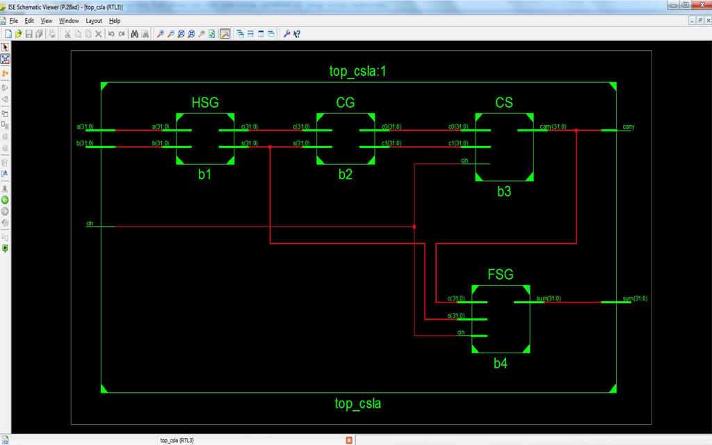
The proposed CSLA adder is a variable length CSLA adder and based on this proposed CSLA we are creating the 256 bit sqrt- CSLA structure. This sqrt CSLA adder is reducing the delay of the architecture. The Proposed CSLA is design with variable length inputs, so it’s flexible to different application. The proposed CSLA structure is as shown in Fig.8. It is composed of one half-sum generation (HSG) unit, one full sum generation (FSG) unit, one carry-generation (CG) unit, and one carry-selection (CS) unit. The CG unit composed of two units namely CGO and CG 1 Corresponding to input-carry ‘0’ and ‘1’, respectively. Input to the HSG unit is two n-bit operands A and B and outputs are half-sum (HS) word So and half-carry (HC) word Co of width n-bit each. CG unit receives both So and Co from HSG unit and gives two n-bit full-carry words co, and c1, corresponds to carry-input ‘0’ and ‘1’ ,respectively. The carry selection unit selects final carry based on the Cin from two anticipated carry words C01 and c11 If Cin = 0 then it selects CO I; otherwise it selects c11 Cout is the MSB of c obtained from CS unit and remaining (n-l) LSBs of CS unit are XORed with (n-l) MSBs of half-sum (so) in the FSG unit to obtain final-sum.
” Thanks for Visit this project Pages – Buy It Soon “
A Three Stage Comparator and Its Modified Version With Fast Speed and Low KickbackFPGA Implementation of Low power and Area Efficient SQRT CSLA
Terms & Conditions:
- Customer are advice to watch the project video file output, before the payment to test the requirement, correction will be applicable.
- After payment, if any correction in the Project is accepted, but requirement changes is applicable with updated charges based upon the requirement.
- After payment the student having doubts, correction, software error, hardware errors, coding doubts are accepted.
- Online support will not be given more than 3 times.
- On first time explanations we can provide completely with video file support, other 2 we can provide doubt clarifications only.
- If any Issue on Software license / System Error we can support and rectify that within end of the day.
- Extra Charges For duplicate bill copy. Bill must be paid in full, No part payment will be accepted.
- After payment, to must send the payment receipt to our email id.
- Powered by NXFEE INNOVATION, Pondicherry.
Payment Method :
- Pay Add to Cart Method on this Page
- Deposit Cash/Cheque on our a/c.
- Pay Google Pay/Phone Pay : +91 9789443203
- Send Cheque through courier
- Visit our office directly
- Pay using Paypal : Click here to get NXFEE-PayPal link
Bank Accounts
HDFC BANK ACCOUNT:
- NXFEE INNOVATION,
HDFC BANK, MAIN BRANCH, PONDICHERRY-605004.
INDIA,
ACC NO. 50200013195971,
IFSC CODE: HDFC0000407.

Reviews
There are no reviews yet.