
Proposed Title :
An Efficient Approach for LUT based RNS FIR Filter for Reconfigurable Applications.
Proposed System:
-
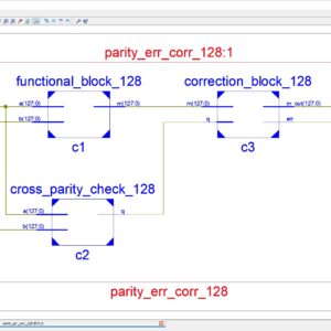
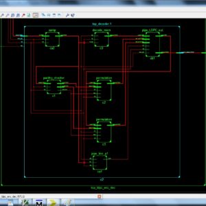
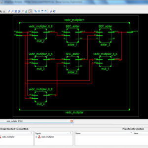
- To Develop a VERILOG code for RNS(Residue Number System) based FIR filter design based on two different approach.
- Type 1 based on the single stage Multiplicative Adder(MA).
- Type 2 based on the multi stage of Multiplicative Adder(MA).
- Added SQRT technique of Conventional Modular adder.
Software implementation:
- Verilog HDL


Reviews
There are no reviews yet.