Discount - 33%

Sharing Logic for Built In Generation of Functional Broadside Tests
Original price was: ₹12,000.00.₹8,000.00Current price is: ₹8,000.00.
Source : VHDL
Abstract:
We are discussed about the built in generation for logic blocks. The advantage of this technique is identifying the similar characteristics of the each logical block. Functional broadside tests are important for addressing overtesting of delay faults as well as avoiding excessive power dissipation during test application. Finally to analysis the performance of the built in generation technique and compare to existing system.
List of the following materials will be included with the Downloaded Backup:
1. Source code ( Modelsim/ Xilinx/ Quartus/ DSCH3/ Microwind)
2. Existing and Proposed Project Comparison
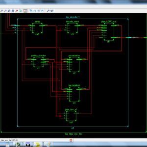
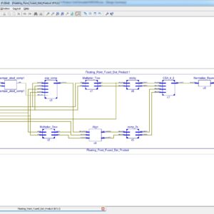
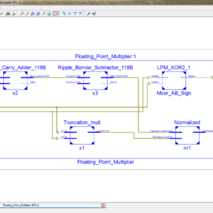
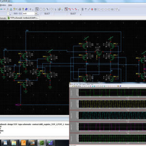
3. Architecture Diagram
4. Algorithm with Flow chart
5. Report for Phase1 and Phase2
6. Proposed abstract document
7. Reference materials
8. Literature survey with Reference Document
9. Online Support ( Team viewer/ Ammy Admin)
Proposed Title :
FPGA Implementation of Sharing Logic for Built In Generation using 3×3 Circuit under test
Proposed System:
- Sharing Logic for Built In Generation, Increase the number of block in the CUT section up to 9 ( 3×3).
Advantages:
- Easy to identify the similar characteristics for the more block.
Software implementation:
- Model sim
- Xilinx 14.2
Related products

 Sharing Logic for Built In Gen...
Original price was: ₹12,000.00.₹8,000.00Current price is: ₹8,000.00.
Reviews
There are no reviews yet.