Proposed Title:
FPGA Implementation of Recursive Approach of Low Power Parallel Self Timed Adder Design
Proposed System:
- Reduced the power consumption compared to the existing architecture
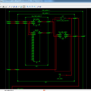
- Simplified the area size 64bit adder is 0.29mW

₹12,000.00 Original price was: ₹12,000.00.₹8,000.00Current price is: ₹8,000.00.
Source : TANNER
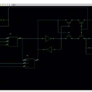
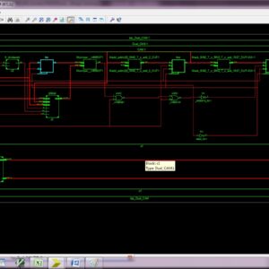
Abstract:
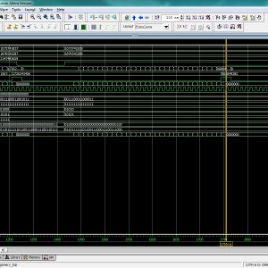
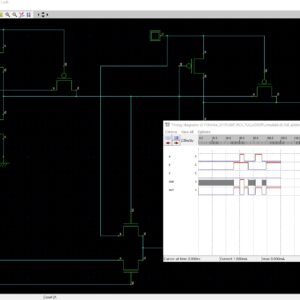
We are briefly discussed about the 64bit parallel self timed adder based on the recursive formulation. The adder is also based on the asynchronous logic circuit and the transistor is connected in parallel. This adder is chance the path automatically, so the delay is configures automatically. The completion detection unit is given the additional support for practical implementation. The simulation is take place with 130nm CMOS technology for the adder circuit. Finally the power consumption for 64bit adder is 0.29mW.
List of the following materials will be included with the Downloaded Backup:
Proposed Title:
Proposed System:
₹16,000.00 Original price was: ₹16,000.00.₹6,000.00Current price is: ₹6,000.00.


₹12,000.00 Original price was: ₹12,000.00.₹8,000.00Current price is: ₹8,000.00.
Copyright © 2024 Nxfee Innovation.
Recursive Approach to the Desi...
₹12,000.00 Original price was: ₹12,000.00.₹8,000.00Current price is: ₹8,000.00.
Reviews
There are no reviews yet.