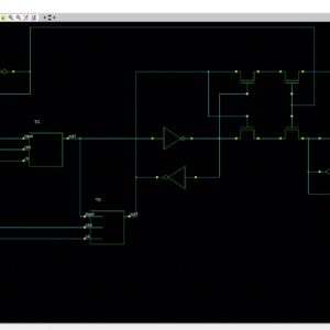
CMOS Implementation of Transmission FF using 21 Transistor Static Topology Shift Register
Proposed System:
-
- Reduced the CMOS 40 nm size to 22 nm
- Reduced the Power consumption compared to existing system
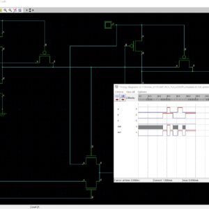
Software implementation:
- TANNER – EDA

₹15,000.00 Original price was: ₹15,000.00.₹10,000.00Current price is: ₹10,000.00.
Source : TANNER – EDA
Abstract:
An extremely low-power flip-flop (FF) named topologically-compressed flip-flop (TCFF) is proposed. As compared with conventional FFs, the FF reduces power dissipation by 75% at 0% data activity. This power reduction ratio is the highest among FFs that have been reported so far. The reduction is achieved by applying topological compression method, merger of logically equivalent transistors to an unconventional latch structure. The very small number of transistors, only three, connected to clock signal reduces the power drastically, and the smaller total transistor count assures the same cell area as conventional FFs. In addition, fully static full-swing operation makes the cell tolerant of supply voltage and input slew variation. An experimental chip design with 40 nm CMOS technology shows that almost all conventional FFs are replaceable with proposed FF while preserving the same system performance and layout area. The proposed design is analysis the power and delay by using tanner tools.
List of the following materials will be included with the Downloaded Backup:
Proposed System:
Software implementation:

₹16,000.00 Original price was: ₹16,000.00.₹6,000.00Current price is: ₹6,000.00.


₹12,000.00 Original price was: ₹12,000.00.₹8,000.00Current price is: ₹8,000.00.
Copyright © 2024 Nxfee Innovation.
A Fully Static Topologically C...
₹15,000.00 Original price was: ₹15,000.00.₹10,000.00Current price is: ₹10,000.00.
Reviews
There are no reviews yet.