
Low Power and Area Efficient Shift Register Using Pulsed Latches
Original price was: ₹14,000.00.₹10,000.00Current price is: ₹10,000.00.
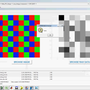
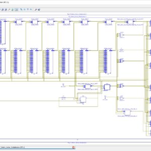
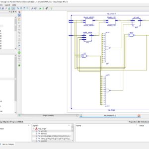
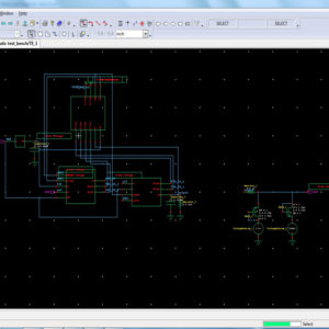
Source Code : Tanner EDA Tool
Abstract:
This paper proposes a low-power and area-efficient shift register using pulsed latches. The area and power consumption are reduced by replacing flip-flops with pulsed latches. This method solves the timing problem between pulsed latches through the use of multiple non-overlap delayed pulsed clock signals instead of the conventional single pulsed clock signal. The shift register uses a small number of the pulsed clock signals by grouping the latches to several sub shifter registers and using additional temporary storage latches. The proposed architecture of this paper analysis the area and power using tanner tool.
List of the following materials will be included with the Downloaded Backup:
Proposed Title:
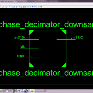
Low Power and Area Efficient Shift Register with CMOS 130nm using Pulsed Latches Flip Flop and Ring counters
Proposed System:
- To Reduced the Power consumption as per the comparison of this base paper.
Advantages:
- Reduced the Power
- Increases the speed
Software used:
- Tanner EDA Tool v13
Related products


 Low Power and Area Efficient S...
Original price was: ₹14,000.00.₹10,000.00Current price is: ₹10,000.00.
Reviews
There are no reviews yet.