
In-Field Test for Permanent Faults in FIFO Buffers of NoC Routers
Original price was: ₹20,000.00.₹10,000.00Current price is: ₹10,000.00.
Source Code : VHDL
Abstract:
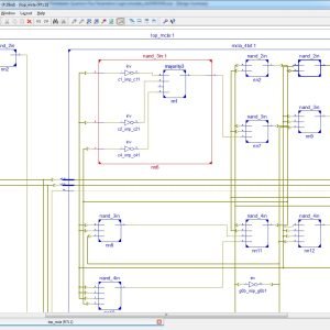
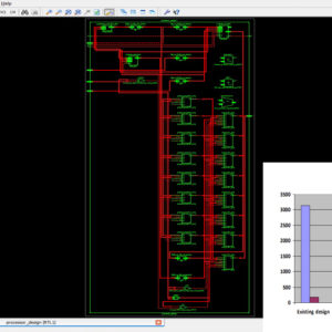
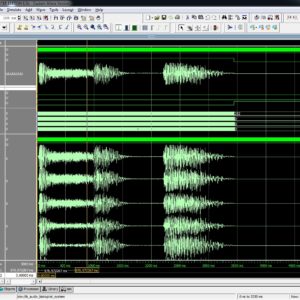
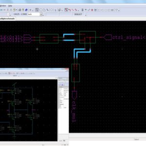
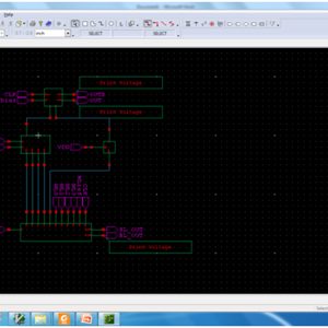
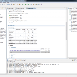
This brief proposes an on-line transparent test technique for detection of latent hard faults which develop in first input first output buffers of routers during field operation of NoC. The technique involves repeating tests periodically to prevent accumulation of faults. A prototype implementation of the proposed test algorithm has been integrated into the router-channel interface and on-line test has been performed with synthetic self-similar data traffic. The performance of the NoC after addition of the test circuit has been investigated in terms of throughput while the area overhead has been studied by synthesizing the test hardware. In addition, an on-line test technique for the routing logic has been proposed which considers utilizing the header flits of the data traffic movement in transporting the test patterns.
List of the following materials will be included with the Downloaded Backup:
Related products

 In-Field Test for Permanent Fa...
Original price was: ₹20,000.00.₹10,000.00Current price is: ₹10,000.00.
Reviews
There are no reviews yet.