Probability-Driven Evaluation of Lower-Part Approximation Adders
Abstract:
Parallel prefix adder topologies suffer from carry chains forming critical paths, limiting the performance and therefore the efficiency. We study approximation methods that offload the lower-part of calculation to an approximate unit and shorten the carry chain. We derive their accuracy models using probability theory. These models can replace Monte Carlo simulations. Furthermore, they can reveal better accuracy trade-offs without going through the RTL design, synthesis, and simulation of each unit and approximation level individually. Thus, they can eliminate the required design and simulation time and effort. After analyzing area-wise comparisons at varying number of approximated bits, we show that choosing a design that outperforms the others probabilistically also outperforms them in terms of accuracy, power, and performance trade-offs.
List of the following materials will be included with the Downloaded Backup:
Quaternary Logic Lookup Table in Standard CMOS
Abstract: Interconnections are increasingly the dominant contributor to delay, area and energy consumption in CMOS digital circuits. The proposed implementation overcomes several limitations found in previous quaternary implementations published so far, such as the need for special features in the CMOS process or power-hungry current-mode cells. We have to use the 512bit quaternary Look Up Table for high level of operations in the FPGA. The proposed architecture of this paper will be planned to implemented and also analysis the output current, output voltage, area using Xilinx 14.3.
List of the following materials will be included with the Downloaded Backup: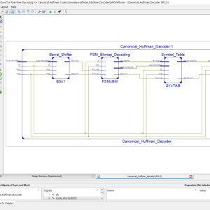
Reconfigurable Architecture for Real-time Decoding of Canonical Huffman Codes
Base Paper Abstract:
Data compression is an important algorithm which has found its use in modern day algorithms such as Convolutional Neural Networks (CNNs). Reconfigurable platforms (like FPGAs) have strong capabilities to implement time complex tasks like CNNs, however, these algorithms present a big challenge due to high resource demand. Data compression is one of the most utilized techniques to reduce memory utilization in FPGAs. The weights of CNN architecture are usually encoded to store in FPGA. In this paper, we propose design of an efficient decoder based on Canonical Huffman that can be utilized for the efficient decompression of weights in CNN. The proposed design makes use of Hash functions to effectively decode the weights eliminating the need for searching dictionary. The proposed design decodes a single weight in a single clock cycle. Our proposed design has a maximum frequency of 408.97MHz utilizing 1% of system LUTs when tested for Aritix 7 platform.
List of the following materials will be included with the Downloaded Backup: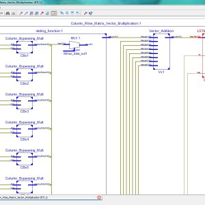
Recurrent Neural Networks With Column-Wise Matrix–Vector Multiplication on FPGAs
Abstract:
This article presents a reconfigurable accelerator for Recurrent Neural networks with fine-grained Column Wise matrix–vector multiplication (RENOWN). We propose a novel latency-hiding architecture for recurrent neural network (RNN) acceleration using column-wise matrix–vector multiplication (MVM) instead of the state-of-the-art row-wise operation. This hardware (HW) architecture can eliminate data dependencies to improve the throughput of RNN inference systems. Besides, we introduce a configurable checkerboard tiling strategy which allows large weight matrices, while incorporating various configurations of element-based parallelism (EP) and vector-based parallelism (VP). These optimizations improve the exploitation of parallelism to increase HW utilization and enhance system throughput. Evaluation results show that our design can achieve over 29.6 tera operations per second (TOPS) which would be among the highest for field-programmable gate array (FPGA)-based RNN designs. Compared to state-of-the-art accelerators on FPGAs, our design achieves 3.7–14.8 times better performance and has the highest HW utilization.
List of the following materials will be included with the Downloaded Backup: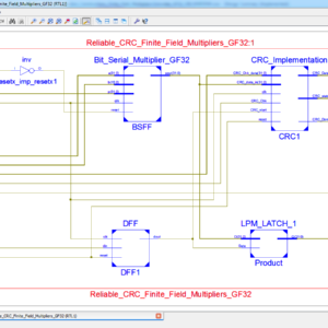
Reliable CRC Based Error Detection Constructions for Finite Field Multipliers With Applications in Cryptography
Abstract:
Finite-field multiplication has received prominent attention in the literature with applications in cryptography and error-detecting codes. For many cryptographic algorithms, this arithmetic operation is a complex, costly, and time-consuming task that may require millions of gates. In this work, we propose efficient hardware architectures based on cyclic redundancy check (CRC) as error-detection schemes for postquantum cryptography (PQC) with case studies for the Luov cryptographic algorithm. Luov was submitted for the National Institute of Standards and Technology (NIST) PQC standardization competition and was advanced to the second round. The CRC polynomials selected are in-line with the required error-detection capabilities and with the field sizes as well. We have developed verification codes through which software implementations of the proposed schemes are performed to verify the derivations of the formulations. Additionally, hardware implementations of the original multipliers with the proposed error-detection schemes are performed over a Xilinx field-programmable gate array (FPGA), verifying that the proposed schemes achieve high error coverage with acceptable overhead.
List of the following materials will be included with the Downloaded Backup:
Reverse Converter Design via Parallel-Prefix Adders: Novel Components, Methodology, and Implementations
Abstract: The implementation of residue number system reverse converters based on well-known regular and modular parallel prefix adders is analyzed. The VLSI implementation results show a significant delay reduction and area × time2 improvements, all this at the cost of higher power consumption, which is the main reason preventing the use of parallel-prefix adders to achieve high-speed reverse converters in nowadays systems. Hence, to solve the high power consumption problem, novel specific hybrid parallel-prefix-based adder components those provide better tradeoff between delay and power consumption. The power, area and delay of the proposed system are analysis using Xilinx 14.2.
List of the following materials will be included with the Downloaded Backup:
Scalable JTAG-Based 32-Bit Memory Test Architecture with MATS+ and MATS++/March-C Fault Detection
Proposed Abstract:
Embedded memories are increasingly used in advanced System-on-Chip (SoC) designs for applications such as networking, automotive control, and medical imaging, where reliability and performance are critical. Ensuring fault-free operation of these memories is essential, yet memory testing remains a major challenge. Conventional MBIST architectures, while effective, often introduce significant silicon overhead, add design complexity, and lack flexibility for post-fabrication updates. In addition, existing memory test algorithms have their own drawbacks: March-C is widely applied and provides high fault coverage, but it requires long test times due to bit-oriented operations and large numbers of read–write cycles; MATS+ is simple and efficient but suffers from lower coverage, particularly for coupling and complex dynamic faults; and MATS++ improves on MATS+ with better detection capability, yet it still trades off hardware cost and scalability when applied to larger 32-bit word-oriented memories. Furthermore, most existing implementations are optimized for small SRAMs and are not easily scalable to clustered embedded memories in SoCs, nor do they fully exploit standard boundary-scan infrastructure for low-cost testing. To address these problems, this work proposes a scalable JTAG-based 32-bit memory test architecture that reuses IEEE 1149.1 boundary-scan resources to apply and compare March-C, MATS+, and MATS++ algorithms in both single-bit and multi-bit test modes. The proposed framework minimizes additional hardware cost by integrating BIST control into boundary-scan registers, while enabling algorithm programmability and flexibility for different memory clusters. The novelty lies in providing a detailed performance comparison of these algorithms under a unified boundary-scan-based architecture, focusing on trade-offs between fault coverage, test time, and silicon overhead. The design is implemented in Verilog HDL and synthesized on an FPGA using Xilinx Vivado, where parameters such as area, power, and latency are evaluated to validate efficiency and practical applicability for SoC-level memory testing.
List of the following materials will be included with the Downloaded Backup: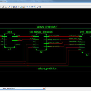
Seizure Prediction using Hilbert Huang Transform on Field Programmable Gate Array
The Hilbert Huang Transform (HHT) has been used extensively in the time-frequency analysis of electroencephalography (EEG) signals and Brain-Computer Interfaces. Most studies utilizing the HHT for extracting features in seizure prediction have used intracranial EEG recordings. Invasive implants in the cortex have unknown long term consequences and pose the risk of complications during surgery. This added risk dimension makes them unsuitable for continuous monitoring as would be the requirement in a Body Area Network. We present an HHT based system on Field Programmable Gate Array (FPGA) for predicting epileptic seizures using scalp EEG. We use bandwidth features of Intrinsic Mode Functions and obtain a classification accuracy of close to 100% using patient-specific classifiers in software. Details of FPGA implementation are also given. The proposed architecture of this paper analysis the logic size, area and power consumption using Xilinx 14.2.
List of the following materials will be included with the Downloaded Backup:
Sharing Logic for Built In Generation of Functional Broadside Tests
Abstract: We are discussed about the built in generation for logic blocks. The advantage of this technique is identifying the similar characteristics of the each logical block. Functional broadside tests are important for addressing overtesting of delay faults as well as avoiding excessive power dissipation during test application. Finally to analysis the performance of the built in generation technique and compare to existing system.
List of the following materials will be included with the Downloaded Backup: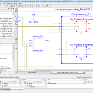
Static Delay Variations Modules For Ripple-Carry and Borrow Save Adders
Abstract:
This paper introduces two statistical delay variability models for certain hardware adder implementations, namely, the ripple-carry adder (RCA) and the borrow-save adder (BSA). The introduced models take into account correlated variation sources. Initially, we derive a first proposed model, namely, Type-I model, in the form of expressions for the computation of the exact Probability Density Functions (PDFS) of maximum output delays for Gaussian and non-Gaussian variation sources. Furthermore, we present closed formulas for the co-variances between output delays of the aforementioned adder architectures. The introduced derived co-variances are subsequently combined with Clark’s method to derive a second proposed model, Type-II model, which comprises approximations of the maximum delay PDF for an RCA and a BSA. Simulation results and the derived exact Type-I PDFs are found to perfectly agree, while the proposed Clark-based Type-II models present an error for standard deviation of maximum delay that increases as BSA word length increases. Both the introduced models and the simulations prove that BSAs achieve narrower delay distributions than RCAs, i.e., they significantly reduce delay variance. Consequently, BSAs are proven to be suitable for variation-tolerant applications by providing a timing safety margin, when compared to RCA architectures. The underlying analysis indicates that for the case of BSA and either intra-die delay variations only or both intra and inter-die delay variations, the Type-II models introduce non negligible errors, which are as much as 16% of the standard deviation of maximum delay for a 256-digit BSA, as the Type II Gaussian PDF approximations deviate significantly from the exact Type-I PDFs. However, for all RCA and BSA inter-die only variation cases, both types present satisfactory accuracy due to the Gaussian shape of exact PDF.
List of the following materials will be included with the Downloaded Backup: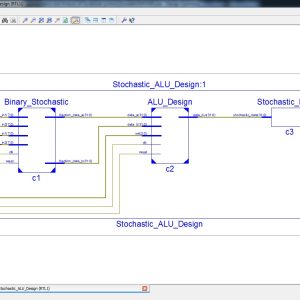
Stochastic Implementation and Analysis of Dynamical Systems Similar to the Logistic Map
Abstract:
Stochastic computing (SC) is a digital computation approach that operates on random bit streams to perform complex tasks with much smaller hardware, with compared to conventional binary radix approaches. It is characterized by its use of pseudo-random numbers implemented by 0-1 sequences called stochastic numbers (SN) are interpreted as probabilities. Accuracy is usually assumed to depend on the interacting SN being highly independent or uncorrelated in a loosely specified way. This paper introduced a new approach of Stochastic and Analysis of Dynamical digital computation with ALU Design. In existing comparison of Floating point ALU Design is not implemented a Stochastic approach, So here the proposed will design to implemented a Stochastic Computing in ALU Design. In top-down design approach of ALU Design, four arithmetic modules, addition, subtraction, multiplication and division are combined to form a Stochastic ALU Unit. Each module is divided into sub-module with two selection bits are combined to select a particular operation. Each module is independent to each other. This modules are realized and validated using VHDL simulation and synthesized in Xilinx 14.2, finally shown the comparison of Area, Power and Delay.
List of the following materials will be included with the Downloaded Backup: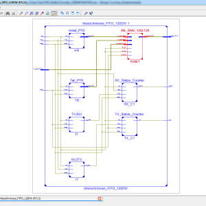
The Mesochronous Dual-Clock FIFO Buffer
Abstract:
To increase system composability and facilitate timing closure, fully synchronous clocking is replaced by more relaxed clocking schemes, such as mesochronous clocking. Under this regime, the modules at the two ends of a mesochronous interface receive the same clock signal, thus operating under the same clock frequency, but the edges of the arriving clock signals may exhibit an unknown phase relationship. In such cases, clock synchronization is needed when sending data across modules. In this brief, we present a novel mesochronous dual-clock first-input– first-output (FIFO) buffer that can handle both clock synchronization and temporary data storage, by synchronizing data implicitly through the explicit synchronization of only the flow-control signals. The proposed design can operate correctly even when the transmitter and the receiver are separated by a long link whose delay cannot fit within the target operating frequency. In such scenarios, the proposed mesochronous FIFO can be extended to support multicycle link delays in a modular manner and with minimal modifications to the baseline architecture. When compared with the other state-of-the-art dual-clock mesochronous FIFO designs, the new architecture is demonstrated to yield a substantially lower cost implementation.
List of the following materials will be included with the Downloaded Backup:
Toward the Multiple Constant Multiplication at Minimal Hardware Cost
Base Paper Abstract:
Multiple Constant Multiplication (MCM) over integers is a frequent operation arising in embedded systems that require highly optimized hardware. An efficient way is to replace costly generic multiplication by bit-shifts and additions, i. e. a multiplier less circuit. In this work, we improve the state of-the-art optimal approach for MCM, based on Integer Linear Programming (ILP). We introduce a new low-level hardware cost metric, which counts the number of one-bit adders and demonstrate that it is strongly correlated with the LUT count. This new model permitted us to consider intermediate truncations that permit to significantly save resources when a full output precision is not required. We incorporate the error propagation rules into our ILP model to guarantee a user-given error bound on the MCM results. The proposed ILP models for multiple flavors of MCM are implemented as an open-source tool and, combined with an automatic code generator, provide a complete coefficient-to-VHDL flow. We evaluate our models in extensive experiments, and propose an in-depth analysis of the impact that design metrics have on synthesized hardware.
List of the following materials will be included with the Downloaded Backup:
Towards Efficient Modular Adders based on Reversible Circuits
Abstract:
Reversible logic is a computing paradigm that has attracted significant attention in recent years due to its properties that lead to ultra-low power and reliable circuits. Reversible circuits are fundamental, for example, for quantum computing. Since addition is a fundamental operation, designing efficient adders is a cornerstone in the research of reversible circuits. Residue Number Systems (RNS) has been as a powerful tool to provide parallel and fault-tolerant implementations of computations where additions and multiplications are dominant. In this paper, for the first time in the literature, we propose the combination of RNS and reversible logic. The parallelism of RNS is leveraged to increase the performance of reversible computational circuits. Being the most fundamental part in any RNS, in this work we propose the implementation of modular adders, namely modulo 2n-1 adders, using reversible logic. Analysis and comparison with traditional logic show that modulo adders can be designed using reversible gates with minimum overhead in comparison to regular reversible adders.
List of the following materials will be included with the Downloaded Backup:
Two Efficient Approximate Unsigned Multipliers by Developing New Configuration for Approximate 4:2 Compressors
Base Paper Abstract:
Approximate computing is a promising approach for reducing power consumption and design complexity in applications that accuracy is not a crucial factor. Approximate multipliers are commonly used in error-tolerant applications. This paper presents three approximate 4:2 compressors and two approximate multiplier designs, aiming at reducing the area and power consumption, while maintaining acceptable accuracy. The paper seeks to develop approximate compressors that align positive and negative approximations for input patterns that have the same probability. Additionally, the proposed compressors are utilized to construct approximate multipliers for different columns of partial products based on the input probabilities of the two compressors in adjacent columns. The proposed approximate multipliers are synthesized using the 28nm technology. Compared to the exact multiplier, the first proposed multiplier improves power × delay and area × power by 91% and 86%, respectively, while the second proposed multiplier improves the two parameters by 90% and 84%, respectively. The performance of the proposed approximate methods was assessed and compared with the existing methods for image multiplication, sharpening, smoothing and edge detection. Also, the performance of the proposed multipliers in the hardware implementation of the neural network was investigated, and the simulation results indicate that the proposed multipliers have appropriate accuracy in these applications.
List of the following materials will be included with the Downloaded Backup:
Variable-Precision Approximate Floating-Point Multiplier for Efficient Deep Learning Computation
Base Paper Abstract:
In this brief, a variable-precision approximate floating-point multiplier is proposed for energy efficient deep learning computation. The proposed architecture supports approximate multiplication with BFloat16 format. As the input and output activations of deep learning models usually follow normal distribution, inspired by the posit format, for numbers with different values, different precisions can be applied to represent them. In the proposed architecture, posit encoding is used to change the level of approximation, and the precision of the computation is controlled by the value of product exponent. For large exponent, smaller precision multiplication is applied to mantissa and for small exponent, higher precision computation is applied. Truncation is used as approximate method in the proposed design while the number of bit positions to be truncated is controlled by the values of the product exponent. The proposed design can achieve 19% area reduction and 42% power reduction compared to the normal BFloat16 multiplier. When applying the proposed multiplier in deep learning computation, almost the same accuracy as that of normal BFloat16 multiplier can be achieved.
List of the following materials will be included with the Downloaded Backup:Provide Wordlwide Online Support
We can provide Online Support Wordlwide, with proper execution, explanation and additionally provide explanation video file for execution and explanations.
24/7 Support Center
NXFEE, will Provide on 24x7 Online Support, You can call or text at +91 9789443203, or email us nxfee.innovation@gmail.com
Terms & Conditions:
Customer are advice to watch the project video file output, and before the payment to test the requirement, correction will be applicable.
After payment, if any correction in the Project is accepted, but requirement changes is applicable with updated charges based upon the requirement.
After payment the student having doubts, correction, software error, hardware errors, coding doubts are accepted.
Online support will not be given more than 3 times.
On first time explanation we can provide completely with video file support, other 2 we can provide doubt clarifications only.
If any Issue on Software license / System Error we can support and rectify that within end of day.
Extra Charges For duplicate bill copy. Bill must be paid in full, No part payment will be accepted.
After payment, to must send the payment receipt to our email id.
Powered by NXFEE INNOVATION, Pondicherry.
Call us today at : +91 9789443203 or Email us at nxfee.innovation@gmail.com
NXFEE Development & Services

Product Categories
- 2014 (11)
- 2015 (39)
- 2016 (30)
- 2017 (16)
- 2018 (17)
- 2019 (42)
- 2020 (29)
- 2021 (17)
- 2022 (23)
- Accessories (43)
- Area Efficient (116)
- High speed VLSI Design (56)
- IEEE (15)
- Image Processing (40)
- Low power VLSI Design (97)
- NOC VLSI Design (2)
- VLSI (249)
- VLSI 2023 (21)
- VLSI 2024 (18)
- VLSI 2025 (30)
- VLSI 2026 (3)
- VLSI Application / Interface and Mini Projects (31)
- VLSI_2023 (15)
Filter by price
Product Status
Sort by rating
Sort by producents

Copyright © 2026 Nxfee Innovation.