Low Power Dual Use of Power Lines for Design for Testability A CMOS Receiver Design
Proposed System:
- Low Power and Area Efficient
Software implementation:
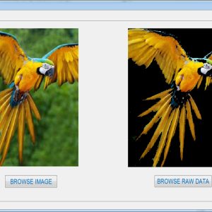
- DSCH3/MICROWIND

₹10,000.00 Original price was: ₹10,000.00.₹6,000.00Current price is: ₹6,000.00.
Source : DSCH3 / MICROWIND
Abstract:
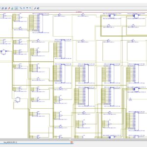
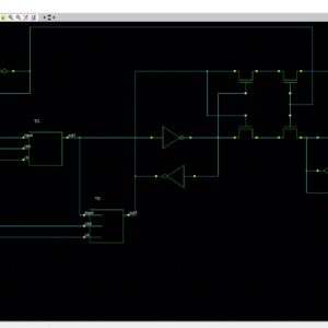
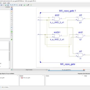
As the circuit complexity increases, the number of internal nodes increases proportionally, and individual internal nodes are less accessible due to the limited number of available I/O pins. To address the problem, we proposed power line communications (PLCs) at the IC level, specifically the dual use of power pins and power distribution networks for application/ observation of test data as well as delivery of power. A PLC receiver presented in this paper intends to demonstrate the proof of concept, specifically the transmission of data through power lines. The main design objective of the proposed PLC receiver is the robust operation under variations and droops of the supply voltage rather than high data speed. The PLC receiver is designed and fabricated in CMOS 0.18-µm technology under a supply voltage of 1.8V.
List of the following materials will be included with the Downloaded Backup:
Proposed System:
Software implementation:
₹12,000.00 Original price was: ₹12,000.00.₹8,000.00Current price is: ₹8,000.00.


₹18,000.00 Original price was: ₹18,000.00.₹10,000.00Current price is: ₹10,000.00.
Copyright © 2024 Nxfee Innovation.
Dual Use of Power Lines for De...
₹10,000.00 Original price was: ₹10,000.00.₹6,000.00Current price is: ₹6,000.00.
Reviews
There are no reviews yet.