Proposed Title :
CMOS Implementation of Low Power and High Performance RF Receiver for WSN
Improvement of this Project:
To implement Trans-conductance LNA (Low Noise Amplifier), Mixer & Local Oscillator Baseband Filter and TIA (Trans-impedance Amplifier).
To implement RF receiver with the help of above listed building blocks.
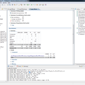
To implement RF receiver at 45 nm and 130 nm CMOS Technology and compared all the parameters in terms of area, delay and power.
Software implementation:
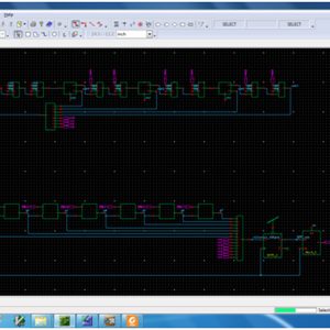
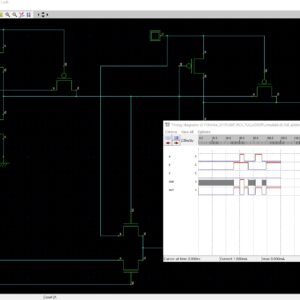
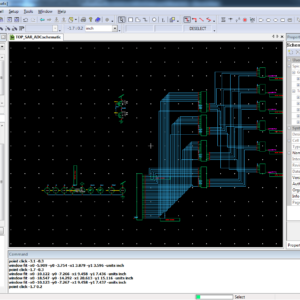
- TANNER EDA
Proposed System:
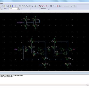
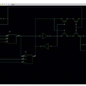
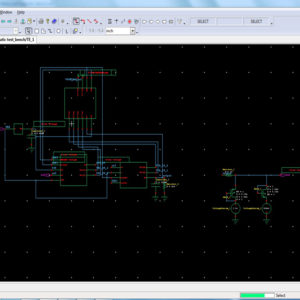
In recent technology of high level signal processing and application will have lot of complexity to transmit and receive a signals in RF (Radio frequency ) based WSN. In this part early RF module will consist of separate blocks for low noise amplifier, mixer and filter with single or double conversion voltage signal processing, for this kind number block will create more critical path, due to these area complexity and power consumption will increases, and it’s not performing good in accuracy. Here this proposed work will present, 900-MHz based RF receiver in one block with local oscillator, mixer, filter, LNA and TIA. This method of proposed architecture will design in Tanner EDA at 130nm and 45nm CMOS technology with perform good in area, delay and power.
” Thanks for Visit this project Pages – Buy It Soon “
Highly Linear Low-Power Wireless RF Receiver for WSN
“Buy VLSI Projects On On-Line”
Terms & Conditions:
- Customer are advice to watch the project video file output, before the payment to test the requirement, correction will be applicable.
- After payment, if any correction in the Project is accepted, but requirement changes is applicable with updated charges based upon the requirement.
- After payment the student having doubts, correction, software error, hardware errors, coding doubts are accepted.
- Online support will not be given more than 3 times.
- On first time explanations we can provide completely with video file support, other 2 we can provide doubt clarifications only.
- If any Issue on Software license / System Error we can support and rectify that within end of the day.
- Extra Charges For duplicate bill copy. Bill must be paid in full, No part payment will be accepted.
- After payment, to must send the payment receipt to our email id.
- Powered by NXFEE INNOVATION, Pondicherry.
Payment Method :
- Pay Add to Cart Method on this Page
- Deposit Cash/Cheque on our a/c.
- Pay Google Pay/Phone Pay : +91 9789443203
- Send Cheque through courier
- Visit our office directly
- Pay using Paypal : Click here to get NXFEE-PayPal link