Proposed Title :
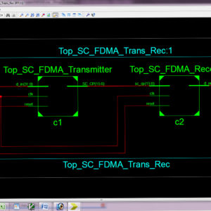
CMOS Implementation of Successive Approximation method of Time Interleaved ADC with 65nm technology
Proposed System:
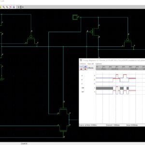
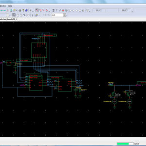
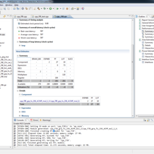
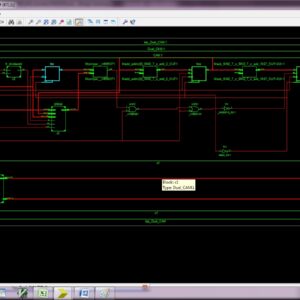
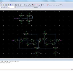
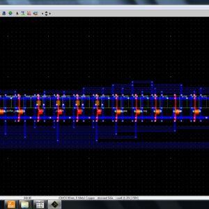
- In this Paper we are designed this work on 65nm CMOS Technology
Software implementation:
- Tanner EDA
” Thanks for Visit this project Pages – Buy It Soon “
A 6-GS/s 6-bit Time Interleaved SAR-ADC
“Buy VLSI Projects On On-Line”
Terms & Conditions:
- Customer are advice to watch the project video file output, before the payment to test the requirement, correction will be applicable.
- After payment, if any correction in the Project is accepted, but requirement changes is applicable with updated charges based upon the requirement.
- After payment the student having doubts, correction, software error, hardware errors, coding doubts are accepted.
- Online support will not be given more than 3 times.
- On first time explanations we can provide completely with video file support, other 2 we can provide doubt clarifications only.
- If any Issue on Software license / System Error we can support and rectify that within end of the day.
- Extra Charges For duplicate bill copy. Bill must be paid in full, No part payment will be accepted.
- After payment, to must send the payment receipt to our email id.
- Powered by NXFEE INNOVATION, Pondicherry.
Payment Method :
- Pay Add to Cart Method on this Page
- Deposit Cash/Cheque on our a/c.
- Pay Google Pay/Phone Pay : +91 9789443203
- Send Cheque through courier
- Visit our office directly
International Payment Method :
- Pay using Paypal : Click here to get NXFEE-PayPal link