Description
Proposed Title :
A 45nm and 65 nm CMOS Implementation Class C/D VCO for Ultralow-power Appliations
Improvement of this Project:
To develop this Class C/D Voltage Control oscillators at 45nm CMOS Technology, at 0.1V with compared and proved the performance of Area, Delay and Power to existing 65nm CMOS Technology.
Software implementation:
- TANNER EDA
Existing System:
VOLTAGE-CONTROLLED oscillators (VCOs) play a key role in modern radio frequency (RF) integrated circuit (IC) multistandard transceivers and, therefore, are subject to continuous research efforts that push the boundaries of their multifaceted performance/power efficiency in the stateof-the-art applications and integration technologies. Usually, different wireless systems have various requirements for the VCO performance. For Internet of Things (IoT) applications, the VCO should maintain a low power consumption, while the phase noise performance can be quite relaxed, e.g., −102 dBc/Hz at 2.5-MHz offset for the Bluetooth low-energy receiver at 2.4-GHz carrier frequency. On the other hand, the cellular applications require very stringent phase noise performance, e.g., −162 dBc/Hz at 20-MHz offset at 900-MHz carrier frequency for the Global System for Mobile transmitter (TX) and −160 dBc/Hz at 30-MHz offset at ∼2-GHz carrier frequency for the long-term evolution/wideband code division multiple access TX.
The design of VCOs is usually time-consuming, even after a particular architecture has been selected. In addition to the phase noise and power consumption, other specifications such as the frequency tuning range and frequency pushing due to the supply voltage variation also need to be carefully considered in a practical design. According to the time-variant phase noise model, for a typical voltage-biased VCO employing crosscoupled nMOS transistors (Fig. 1) oscillating at ω0, its phase noise at offset frequency ω can be expressed as
where Q is the tank quality factor, VP is the differential output amplitude, C is the total tank capacitance, T,rms is the rms impulse sensitivity functions of the parallel resistance representing the conversion from tank thermal noise to phase noise, and F is the noise factor defined by the ratio between the total phase noise and the phase noise induced by the tank loss. To meet the phase noise requirement at a certain frequency, a proper tank capacitance C and inductance L need to be chosen. However, it is difficult to obtain accurate values for C and L using (1) since the values of F depend on the working mode of M1/M2, related to the gate-biasing voltage and transistor sizes.
If taking the noise contributions for the transistor channel conductance (GDS) into consideration, the situation becomes even more complex. Furthermore, for each iteration, when the L value is changed, the switchedcapacitor array (SCA) and varactors also need to be redesigned to meet the frequency-tuning range requirement, which would change the tank Q and, in turn, affect the phase noise performance. In the practical design, even more iterations are required to guarantee satisfactory VCO performances in the presence of process, voltage, and temperature variations. The recent works also reveal that the phase noise and frequency pushing can be improved by utilizing the commonmode resonance at the double-oscillation frequency, which requires extra design efforts to balance the differential-mode and common-mode tank inductances and capacitances. Thus, numerous nonsystematic iterations are inevitable to attain high-quality designs.
Disadvantages:
- More Phase noise
- More power consumption
- More iterations are required to give performance in voltage and temperature variations.
Proposed System:
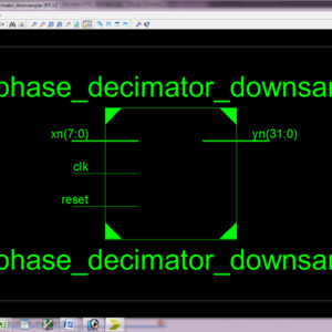
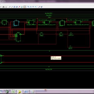
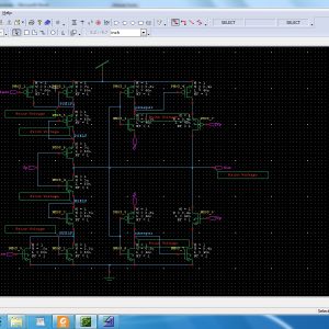
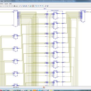
In this paper performance boundaries and corresponding tradeoffs of a complex dual-mode class-C/D voltage controlled oscillator (VCO) it will play a major key role in modern radio frequency of integrated circuit with multi standard transceivers and receivers. These VCO embedded in the state of the art multi standard transceivers must comply with extremely high performance and ultra low power requirements for modern cellular and internet of things applications, and it’s should maintain low power consumptions while the phase noise performance can be quite relaxed. Here, the paper presents the dual mode design and optimization of complex dual mode class C/D VCO will integrated with 5 MHZ ~ 10 MHz frequency range with 0.1V to 0.3V with perform in the CMOS technology of 45nm and 64nm. Finally this work will designed in Tanner EDA tool and proved the comparisons of low power consumptions in difference of 45nm and 65nm CMOS technology.
To overcome the difficulties found on the manual sizing of RF IC blocks, different optimization-based sizing approaches were developed. These EDA tools use algorithms that efficiently explore the design space, instead of iterating over designer-defined analytical equations. They can be applied over performance models that capture several circuits and inductor characteristics of the RF circuits and, particularly, VCOs and however, the use of foundry-provided device models and a circuit simulator as an evaluation engine, i.e., simulation-based sizing, proved to be the most accurate and widely adopted approach for RF, despite its increased computational effort. There are several commercially available solutions, e.g., Cadence’s Virtuoso GXL or MunEDA’s DNO/GNO that also follows the simulationbased architecture, and while useful, most of these tools still take a limitative single-objective approach being used mostly to adjust the manual sizing in a semiautomated manner. Therefore, these simulation-based methodologies are continuously subject to research efforts by the research community to cope with the most recent design challenges.
Developed methodologies are usually applied to simpler VCO topologies for a small number of design variables and considering only a small set of performance figures. To exemplify, in, the cross-coupled double-differential VCO was optimized for a 4-D performance space (oscillation frequency fosc, phase noise, power, and oscillation amplitude OscAmp). The optimization was done on a 7-D design variable space. On the other hand, in, the VCO was optimized for a 9-D performance space (frequency-tuning range, phase noises, power, OscAmp, and area). In this case, a 9-D design variable space was considered. In other works, the performance and design variable spaces are similar, and hardcoded formulas are used to compute other metrics, e.g., figure of merit (FOM). Following, when faced with a complex real-world VCO design, designers in both academic and industrial environments end up using EDA tools to solve only subproblems of the manual design, i.e., change only a subset of the design variables x to tackle local optimization (LO) targets, as illustrated in Fig. 2(b). This mixed iterative/sequential optimization design approach leads to suboptimal solutions, as the tradeoffs between conflicting performance figures are not properly weighted. Therefore, for modern VCO applications, this approach does not fit, as more complex topologies and a wider set of requirements must be balanced simultaneously, e.g., multimode operation, digitally controlled frequency-tuning ranges, or attain a limited frequency pushing due to supply voltage variation.
This paper applies and adapts an EDA framework to bypass the difficulties faced on the sizing of complex RF IC blocks and, particularly, a dual-mode class-C/D VCO. The major contributions of this paper can be summarized as follows.
1) Adoption of an EDA framework to fully optimize a complex class-C/D VCO for the state-of-the-art IoT and cellular specifications.
2) Study and discussion of the possibility to meet extreme operational requirements in a single optimization run with the same framework setup, by analyzing the complete tradeoffs between power consumption, phase noise, and frequency pushing, obtained with a many-objective optimization. A study that is impossible to perform using commercially available solutions.
3) Unlike previous research works in VCO sizing optimization, here, the circuit’s performance space greatly surpasses what can be found on EDA solutions in the literature. Two human-untreatable 18-D and 66-D performance spaces, defined over two different modes, i.e., worst case mode in typical conditions and worst case mode in worst case corner (WCC) conditions, respectively, for the same 28-D design variable space that affects the sizing of 43 devices (RF and digital components).
Figure 2 : (a) Knowledge-based manual design. (b) Mixed iterative/sequential optimization design approach. (c) Adopted optimize “everything-at-once” approach, where x is the design variables’ array
4) The adopted automatic design methodology is built over the established all-inclusive test bench formulation for optimization-based RF IC sizing but enhanced with parsers for the native output formats of most widely used off-the-shelf simulators and a comprehensive set of postprocessing options. As such, the proposed formulation enables the optimize “everything-at-once” approach of Fig. 2(c), leading to a more systematic design flow that reduces the risk of bad design decisions while balancing all the design challenges simultaneously. III. PRELIMINARIES This section reviews important concepts for analog and RF IC automation, i.e., the optimization-based sizing and all-inclusive test bench formulation.
- Optimization-Based Rf Ic Sizing In the traditional optimization-based sizing, the kernel is responsible for proposing P different sizing solutions for circuit simulation, each one with a new set of x design variables (e.g., devices’ widths, lengths, and number of fingers) and is set to solve the constrained many-objective problem find x that min fm(x) m = 1,
- 2,… M s.t. g j(x) ≥ 0 j = 1, 2,… J x L i ≤ xi ≤ xU i i = 1, 2,… N (2) where x is the vector of N design variables, g(x) is the J constraint functions, and the output is a Pareto-optimal front (POF) representing the tradeoffs between M objective functions f (x). In this problem, the number of design variables defines the search space order, while the variable ranges (minimum, maximum, and step values) define the size of the search space.
Advantages:
- Less Phase noise
- Less power consumption
- Less iterations are required to give performance in voltage and temperature variations.
” Thanks for Visit this project Pages – Buy It Soon “
Many-Objective Sizing Optimization of a Class-C/D VCO for Ultralow-Power IoT and Ultralow Phase-Noise Cellular Applications
“Buy VLSI Projects On On-Line”
Terms & Conditions:
- Customer are advice to watch the project video file output, before the payment to test the requirement, correction will be applicable.
- After payment, if any correction in the Project is accepted, but requirement changes is applicable with updated charges based upon the requirement.
- After payment the student having doubts, correction, software error, hardware errors, coding doubts are accepted.
- Online support will not be given more than 5 times.
- Extra Charges For duplicate bill copy. Bill must be paid in full, No part payment will be accepted.
- After payment, to must send the payment receipt to our email id.
- Powered by NXFEE INNOVATION, Pondicherry.
Payment Method:
- Pay Add to Cart Method on this Page
- Deposit Cash/Cheque on our a/c.
- Pay Google Pay/Phone Pay : +91 9789443203
- Send Cheque through courier
- Visit our office directly
International Payment Method:
- Pay using Paypal : Click here to get NXFEE-PayPal link
Bank Accounts
HDFC BANK ACCOUNT:
- NXFEE INNOVATION,
HDFC BANK, MAIN BRANCH, PONDICHERRY-605004.
INDIA,
ACC NO. 50200013195971,
IFSC CODE: HDFC0000407.