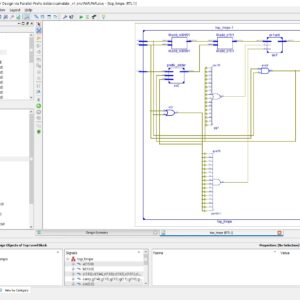
Proposed System:
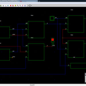
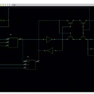
- Extended the architecture up to Four Bit Adder using 16:1 Multiplexer
- Possible to design the QLUT ALU Design
Advantages:
- Occupied Less Area
- low power consumption
Software implementation:
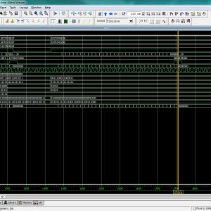
- Modelsim
- Xilinx ISE

₹16,000.00 Original price was: ₹16,000.00.₹8,000.00Current price is: ₹8,000.00.
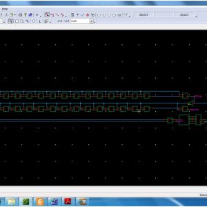
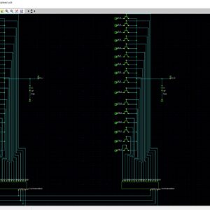
Source : VHDL & MICROWIND
Abstract:
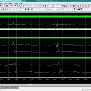
Interconnections are increasingly the dominant contributor to delay, area and energy consumption in CMOS digital circuits. The proposed implementation overcomes several limitations found in previous quaternary implementations published so far, such as the need for special features in the CMOS process or power-hungry current-mode cells. We have to use the 512bit quaternary Look Up Table for high level of operations in the FPGA.The proposed architecture of this paper will be planned to implemented and also analysis the output current, output voltage, area using Xilinx 14.3.
List of the following materials will be included with the Downloaded Backup:
Proposed System:
Advantages:
Software implementation:
₹20,000.00 Original price was: ₹20,000.00.₹14,000.00Current price is: ₹14,000.00.


₹10,000.00 Original price was: ₹10,000.00.₹6,000.00Current price is: ₹6,000.00.
Copyright © 2026 Nxfee Innovation.
Quaternary Logic Lookup Table ...
₹16,000.00 Original price was: ₹16,000.00.₹8,000.00Current price is: ₹8,000.00.
Reviews
There are no reviews yet.