₹16,000.00Original price was: ₹16,000.00.₹6,000.00Current price is: ₹6,000.00.
Source Code : TANNERAbstract:
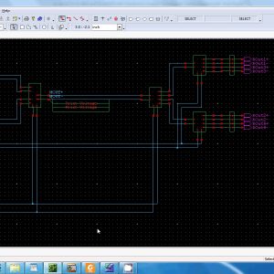
This paper explores the use of transformer-coupled (TC) technique for the 2:1 MUX and the 1:2 DEMUX to serialize-and-deserialize (SerDes) high-speed data sequence. The widely used current-mode logic (CML) designs of latch and multiplexer/demultiplexer (MUX/DEMUX) are replaced by the proposed TC approach to allow the more headroom and to lower the power consumption. Through the stacked transformer, the input clock pulls down the differential source voltage of the TC latch and the TC multiplexer core while alternating between the two-phase operations. With the enhanced drain-source voltage, the TC design attracts more drain current with less width-to-length ratio of NMOS than that of the CML counterpart. The source-offset voltage is decreased so that the supply voltage can be reduced. The lower supply voltage improves the power consumption and facilitates the integration with low voltage supply SerDes interface. The MUX and the DEMUX chips are fabricated in 65-nm standard CMOS process and operate at 0.7-V supply voltage. The chips are measured up to 40-Gb/s with sub-hundred milliwatts power consumption.
List of the following materials will be included with the Downloaded Backup:
₹16,000.00Original price was: ₹16,000.00.₹6,000.00Current price is: ₹6,000.00.
Source Code : TANNERAbstract:
A duty-cycle correction technique using a novel pulse width modification cell is demonstrated across a frequency range of 100 MHz–3.5 GHz. The technique works at frequencies where most digital techniques implemented in the same technology node fail. An alternative method of making time domain measurements such as duty cycle and rise/fall times from the frequency domain data is introduced. The data are obtained from the equipment that has significantly lower bandwidth than required for measurements in the time domain. An algorithm for the same has been developed and experimentally verified. The correction circuit is implemented in a 0.13-µm CMOS technology and occupies an area of 0.011 mm2. It corrects to a residual error of less than 1%. The extent of correction is limited by the technology at higher frequencies. The proposed architecture of this paper area and power consumption analysis using tanner tool.
List of the following materials will be included with the Downloaded Backup:
₹20,000.00Original price was: ₹20,000.00.₹10,000.00Current price is: ₹10,000.00.
Source Code : VHDL
Abstract:
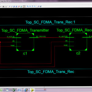
A novel low-complexity multiple-input multiple-output (MIMO) detector tailored for single-carrier frequency division-multiple access (SC-FDMA) systems, suitable for efficient hardware implementations. The proposed detector starts with an initial estimate of the transmitted signal based on a minimum mean square error (MMSE) detector. Subsequently, it recognizes less reliable symbols for which more candidates in the constellation are browsed to improve the initial estimate. The proposed architecture of this paper analysis the logic size, area and power consumption using Xilinx 14.2.
List of the following materials will be included with the Downloaded Backup:
₹14,000.00Original price was: ₹14,000.00.₹10,000.00Current price is: ₹10,000.00.
Source Code : VHDL
Abstract:
Iterative methods are basic building blocks of communication systems and often represent a dominating part of the system, and therefore, they necessitate careful design and implementation for optimal performance. In this brief, we propose a novel field programmable gate arrays design of matrix–vector multiplier that can be used to efficiently implement widely adopted iterative methods. The proposed design exploits the sparse structure of the matrix as well as the fact that spreading code matrices have equal magnitude entries. Implementation details and timing analysis results are promising and are shown to satisfy most modern communication system requirements.
List of the following materials will be included with the Downloaded Backup:
₹10,000.00Original price was: ₹10,000.00.₹6,000.00Current price is: ₹6,000.00.
Source Code : VHDL
Abstract:
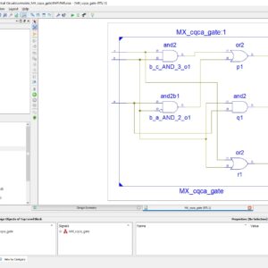
In this paper, we propose the design of two vectors testable sequential circuits based on conservative logic gates. The proposed sequential circuits based on conservative logic gates outperform the sequential circuits implemented in classical gates in terms of testability. Any sequential circuit based on conservative logic gates can be tested for classical unidirectional stuck-at faults using only two test vectors. The two test vectors are all 1s, and all 0s. The designs of two vectors testable latches, master-slave flip-flops and double edge triggered (DET) flip-flops are presented. The importance of the proposed work lies in the fact that it provides the design of reversible sequential circuits completely testable for any stuck-at fault by only two test vectors, thereby eliminating the need for any type of scan-path access to internal memory cells. The reversible design of the DET flip-flop is proposed for the first time in the literature. We also showed the application of the proposed approach toward 100% fault coverage for single missing/additional cell defect in the quantum dot cellular automata (QCA) layout of the Fredkin gate. We are also presenting a new conservative logic gate called multiplexer conservative QCA gate (MX-cqca) that is not reversible in nature but has similar properties as the Fredkin gate of working as 2:1 multiplexer. The proposed MX-cqca gate surpasses the Fredkin gate in terms of complexity (the number of majority voters), speed, and area.
List of the following materials will be included with the Downloaded Backup:
₹16,000.00Original price was: ₹16,000.00.₹6,000.00Current price is: ₹6,000.00.
Source Code : TANNERAbstract:
Ring oscillators (ROs) are popular due to their small area, modest power, wide tuning range, and ease of scaling with process technology. However, their use in many applications is limited due to poor phase noise and jitter performance. Thermal noise and flicker noise contribute jitter that decreases inversely with oscillation frequency. This paper describes a frequency boost technique to reduce jitter in ROs. We boost the internal oscillation frequency and introduce a frequency divider following the oscillator to maintain the desired output frequency. This approach offers reduced jitter as well as the opportunity to trade off output jitter with power for dynamic performance management. The oscillator has 32 operating modes, corresponding to different values for the ring size and frequency division. In a 0.5-µm CMOS process, the highest oscillation frequency achieved is 25 MHz with a root-mean-square period jitter of 54 ps and a power consumption of 817 µW at 5 V supply. A jitter model for current-starved oscillators was derived and verified by measurement; a direct relationship between oscillation frequency and jitter was derived and measured. Compared with other oscillators, this design achieves the highest performance in terms of jitter per unit interval and figure-of-merit. The performance is expected to improve in more advanced technologies. The results are summarized to offer design guidance based on the frequency boost technique. The proposed architecture of this paper area and power consumption analysis using tanner tool.
List of the following materials will be included with the Downloaded Backup:
₹20,000.00Original price was: ₹20,000.00.₹10,000.00Current price is: ₹10,000.00.
Source Code : VHDL
Abstract:
This brief proposes an on-line transparent test technique for detection of latent hard faults which develop in first input first output buffers of routers during field operation of NoC. The technique involves repeating tests periodically to prevent accumulation of faults. A prototype implementation of the proposed test algorithm has been integrated into the router-channel interface and on-line test has been performed with synthetic self-similar data traffic. The performance of the NoC after addition of the test circuit has been investigated in terms of throughput while the area overhead has been studied by synthesizing the test hardware. In addition, an on-line test technique for the routing logic has been proposed which considers utilizing the header flits of the data traffic movement in transporting the test patterns.
List of the following materials will be included with the Downloaded Backup:
₹14,000.00Original price was: ₹14,000.00.₹10,000.00Current price is: ₹10,000.00.
Source Code : Tanner EDA Tool
Abstract:
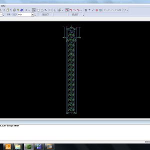
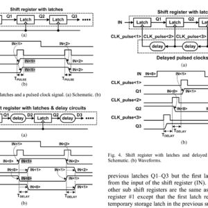
This paper proposes a low-power and area-efficient shift register using pulsed latches. The area and power consumption are reduced by replacing flip-flops with pulsed latches. This method solves the timing problem between pulsed latches through the use of multiple non-overlap delayed pulsed clock signals instead of the conventional single pulsed clock signal. The shift register uses a small number of the pulsed clock signals by grouping the latches to several sub shifter registers and using additional temporary storage latches. The proposed architecture of this paper analysis the area and power using tanner tool.
List of the following materials will be included with the Downloaded Backup:
₹16,000.00Original price was: ₹16,000.00.₹10,000.00Current price is: ₹10,000.00.
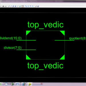
Source Code : VHDLAbstract:
Vedic mathematics is a unique technique of carrying out mathematical computations and it has its roots in the ancient Indian Mathematics. This paper presents the divider architecture using one of the Vedic mathematics techniques called as Paravartya-Yojayet, which means to transpose and apply. This paper proposes a fast, low power and cost effective architecture of a divider using the ancient Indian Vedic division algorithm. The merits of the proposed architecture are proved by comparing the gate count, power consumption and delay against the conventional divider architectures. The proposed architecture of this paper analysis the logic size, area and power consumption using Xilinx 14.2.
List of the following materials will be included with the Downloaded Backup:
₹16,000.00Original price was: ₹16,000.00.₹6,000.00Current price is: ₹6,000.00.
Source Code : TANNER/HSPICEAbstract:
Emerging nonvolatile memories (NVMs), such as MRAM, PRAM, and RRAM, have been widely investigated to replace SRAM as the configuration bits in field-programmable gate arrays (FPGAs) for high security and instant power ON. However, the variations inherent in NVMs and advanced logic process bring reliability issue to FPGAs. This brief introduces a low-power variation-tolerant nonvolatile lookup table (nvLUT) circuit to overcome the reliability issue. Because of large ROFF/RON, 1T1R RRAM cell provides sufficient sense margin as a configuration bit and a reference resistor. A single-stage sense amplifier with voltage clamp is employed to reduce the power and area without impairing the reliability. Matched reference path is proposed to reduce the parasitic RC mismatch for reliable sensing. Evaluation shows that 22% reduction in delay, 38% reduction in power, and the tolerance of variations of 2.5× typical RON or ROFF in reliability are achieved for proposed nvLUT with six inputs. The proposed architecture of this paper area and power consumption analysis using tanner tool.
List of the following materials will be included with the Downloaded Backup:
₹16,000.00Original price was: ₹16,000.00.₹6,000.00Current price is: ₹6,000.00.
Source Code : TANNERAbstract:
Design of a low-energy power-ON reset (POR) circuit is proposed to reduce the energy consumed by the stable supply of the dual supply static random access memory (SRAM), as the other supply is ramping up. The proposed POR circuit, when embedded inside dual supply SRAM, removes its ramp-up constraints related to voltage sequencing and pin states. The circuit consumes negligible energy during ramp-up, does not consume dynamic power during operations, and includes hysteresis to improve noise immunity against voltage fluctuations on the power supply. The POR circuit, designed in the 40-nm CMOS technology within 10.6-µm2 area, enabled 27× reduction in the energy consumed by the SRAM array supply during periphery power-up in typical conditions. The proposed architecture of this paper area and power consumption analysis using tanner tool.
List of the following materials will be included with the Downloaded Backup:
₹16,000.00Original price was: ₹16,000.00.₹10,000.00Current price is: ₹10,000.00.
Source Code : VHDL
Abstract:
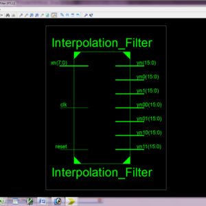
The input-matrix and the coefficient-matrix resizes when changes. An analysis of interpolation filter computation for different up-sampling factors is made in this paper to identify redundant computations and removed those by reusing partial results. Reuse of partial results eliminates the necessity of matrix resizing in interpolation filter computation. A novel block-formulation is presented to share the partial results for parallel computation of filter outputs of different up-sampling factors. Using the proposed block formulation, to increase the number of tab to 16 and to get the accuracy and reduce the delay. The proposed architecture of this paper analysis the logic size, area and power consumption using Xilinx 14.2.
List of the following materials will be included with the Downloaded Backup:
₹15,000.00Original price was: ₹15,000.00.₹6,000.00Current price is: ₹6,000.00.
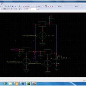
Source Code : TANNERAbstract:
In this paper, a new design procedure has been proposed for realization of logarithmic function via three phases: 1) differentiation; 2) division; and 3) integration for any arbitrary analog signal. All the basic building blocks, i.e., differentiator, divider, and integrator, are realized by operational transconductance amplifier, a current mode device. Realization of exponential, power law and hyperbolic function as the design examples claims that the proposed synthesis procedure has the potential to design a log-based nonlinear system in a systematic and hierarchical manner. The proposed architecture of this paper area and power consumption analysis using tanner tool.
List of the following materials will be included with the Downloaded Backup:
₹16,000.00Original price was: ₹16,000.00.₹10,000.00Current price is: ₹10,000.00.
Source Code : VHDL
Abstract:
The implementation of residue number system reverse converters based on well-known regular and modular parallel prefix adders is analyzed. The VLSI implementation results show a significant delay reduction and area × time2 improvements, all this at the cost of higher power consumption, which is the main reason preventing the use of parallel-prefix adders to achieve high-speed reverse converters in nowadays systems. Hence, to solve the high power consumption problem, novel specific hybrid parallel-prefix-based adder components those provide better tradeoff between delay and power consumption. The power, area and delay of the proposed system are analysis using Xilinx 14.2.
List of the following materials will be included with the Downloaded Backup:
₹16,000.00Original price was: ₹16,000.00.₹10,000.00Current price is: ₹10,000.00.
Source Code : VHDL
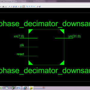
Abstract:
Multirate technique is necessary for systems with different input and output sampling rates. Recent advances in mobile computing and communication applications demand low power and high speed VLSI DSP systems. In this paper to discuss the downsampling technique and its improvement, major drawbacks of present approaches possible to increase degeneracy. This Multirate design methodology is systematic and applicable to many problems. The proposed architecture of this paper analysis the logic size, area and power consumption using Xilinx 14.2.The proposed architecture of this paper analysis the logic size, area and power consumption using Xilinx 14.2.
List of the following materials will be included with the Downloaded Backup:
We can provide Online Support Wordlwide, with proper execution, explanation and additionally provide explanation video file for execution and explanations.
24/7 Support Center
NXFEE, will Provide on 24x7 Online Support, You can call or text at +91 9789443203, or email us nxfee.innovation@gmail.com
Terms & Conditions:
Customer are advice to watch the project video file output, and before the payment to test the requirement, correction will be applicable.
After payment, if any correction in the Project is accepted, but requirement changes is applicable with updated charges based upon the requirement.
After payment the student having doubts, correction, software error, hardware errors, coding doubts are accepted.
Online support will not be given more than 3 times.
On first time explanation we can provide completely with video file support, other 2 we can provide doubt clarifications only.
If any Issue on Software license / System Error we can support and rectify that within end of day.
Extra Charges For duplicate bill copy. Bill must be paid in full, No part payment will be accepted.
After payment, to must send the payment receipt to our email id.
Powered by NXFEE INNOVATION, Pondicherry.
Call us today at : +91 9789443203 or Email us at nxfee.innovation@gmail.com