
Proposed Title :
A 45-nm CMOS Constant Current Source with Reduced PVT Variation
Software implementation:
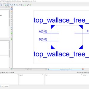
- Tanner EDA
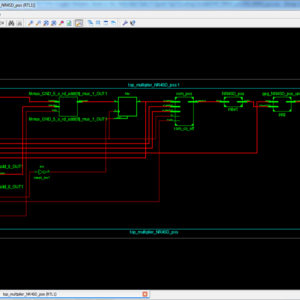
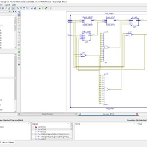
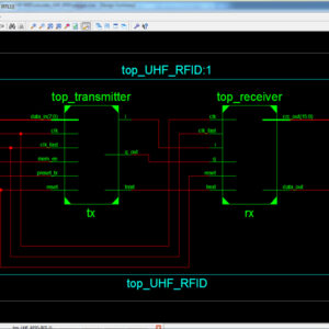
Proposed System:
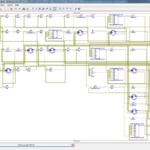
Time to Digital Converter provides the digital representation of time when it occurs. The major requirements for main stream applications include wide measurement range, high resolution, low cost and low process, voltage and temperature (PVT) sensitivity. To achieve resolutions better than 10 ps, most TDCs are implemented in application-specific integrated circuits (ASIC), which is ineffective. Therefore, This paper proposes the new concept of Time-to-digital Converter(TDC) FPGA with high resolution of 2ps(picoseconds) bin size. This concept increases the performance of TDC in order to achieve a high resolution. In this concept the signals are sampled with n number of times and timing reference is generated by feeding original clock into tapped delay line. According to periodicity, the delays among those timing references are wrapped into a single reference period and the effective TDC resolution can be made much smaller than the clock period to compete even with the state-of the art full-custom TDCs in performance. Finally, this concept of High resolution of TDC is implemented in the VERILOG and Synthesized using XILINX and shown the comparison in terms of delay, power and area reports.
” Thanks for Visit this project Pages – Buy It Soon “
A High Resolution FPGA TDC Converter with 2.5 ps Bin Size and -3.79~6.53 LSB Integral Non linearity
Terms & Conditions:
- Customer are advice to watch the project video file output, before the payment to test the requirement, correction will be applicable.
- After payment, if any correction in the Project is accepted, but requirement changes is applicable with updated charges based upon the requirement.
- After payment the student having doubts, correction, software error, hardware errors, coding doubts are accepted.
- Online support will not be given more than 3 times.
- On first time explanations we can provide completely with video file support, other 2 we can provide doubt clarifications only.
- If any Issue on Software license / System Error we can support and rectify that within end of the day.
- Extra Charges For duplicate bill copy. Bill must be paid in full, No part payment will be accepted.
- After payment, to must send the payment receipt to our email id.
- Powered by NXFEE INNOVATION, Pondicherry.
Payment Method :
- Pay Add to Cart Method on this Page
- Deposit Cash/Cheque on our a/c.
- Pay Google Pay/Phone Pay : +91 9789443203
- Send Cheque through courier
- Visit our office directly
- Pay using Paypal : Click here to get NXFEE-PayPal link


Reviews
There are no reviews yet.