
Area-Efficient Bidirectional Shift-Register Using Bidirectional Pulsed-Latches
Original price was: ₹25,000.00.₹10,000.00Current price is: ₹10,000.00.
Source : VHDL
Abstract:
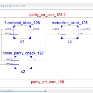
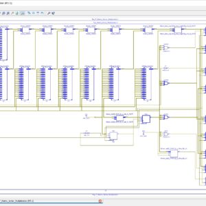
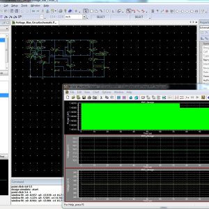
This paper proposes an area-efficient bidirectional shift-register using bidirectional pulsed-latches. The proposed bidirectional shift-register reduces the area and power consumption by replacing master-slave flip-flops and 2-to-1 multiplexers with the proposed bidirectional pulsed-latches and non-overlap delayed pulsed clock signals, and by using sub shift-registers and extra temporary storage latches. A 256-bit bidirectional shift-register was fabricated using a 65nm CMOS process. Its area was 1,943μm2 and its power consumption is 200μW at a 100MHz clock frequency with VDD=1.2V. It reduces area by 39.2% and power consumption by 19.4% compared to the conventional bidirectional shift-register, length in most cases.
List of the following materials will be included with the Downloaded Backup:
Related products

 Area-Efficient Bidirectional S...
Original price was: ₹25,000.00.₹10,000.00Current price is: ₹10,000.00.