FPGA Implementation of Low Power OFDM Baseband Transceiver using VIRTEX-6 FPGA Family
Proposed System:
- Reduced the power consumption
- Reduced the LUT Size
Software implementation:
- Modelsim
- XILINX

₹25,000.00 Original price was: ₹25,000.00.₹10,000.00Current price is: ₹10,000.00.
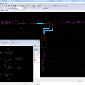
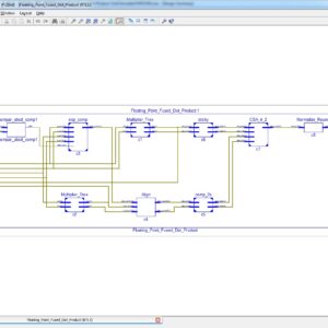
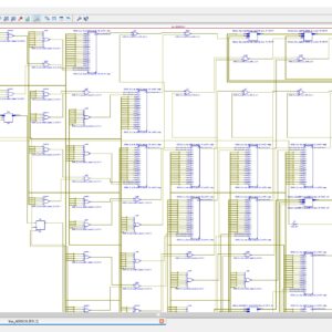
Source : VHDL
Abstract:
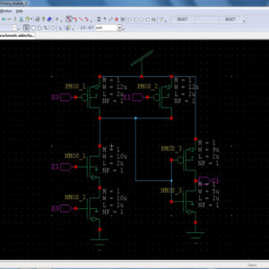
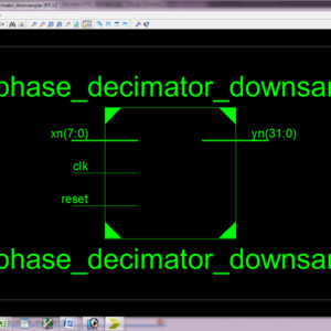
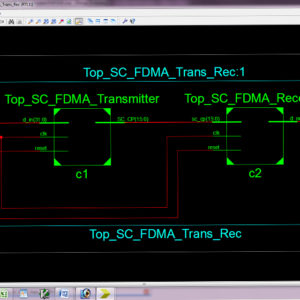
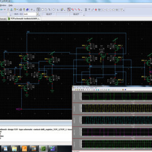
Broadband Wireless Access (BWA) is a successful technology which offers high speed voice, internet connection and video. One of the leading candidates for Broadband Wireless Access is Wi-MAX; it is a technology that compiles with the IEEE 802.16 family of standards. This paper mainly focused towards the hardware Implementation of Wireless MAN-OFDM Physical Layer of IEEE Std 802.16d Baseband Transceiver on FPGA. The RTL coding of VHDL was used, which provides a high level design-flow for developing and validating the communication system protocols and it provides flexibility of changes in future in order to meet real world performance evaluation. This proposed system is analysis area and power. Also the outputs are verified using Xilinx 14.2.
List of the following materials will be included with the Downloaded Backup:
₹20,000.00 Original price was: ₹20,000.00.₹10,000.00Current price is: ₹10,000.00.


₹16,000.00 Original price was: ₹16,000.00.₹10,000.00Current price is: ₹10,000.00.
Copyright © 2026 Nxfee Innovation.
Design and Development of OFDM...
₹25,000.00 Original price was: ₹25,000.00.₹10,000.00Current price is: ₹10,000.00.