Proposed System:
- Reduced the Power consumption.
- Reduce the area size
Software Implementation:
- DSCH3
- MICROWIND
Hardware Implementation:
- ASIC
₹10,000.00 Original price was: ₹10,000.00.₹8,000.00Current price is: ₹8,000.00.
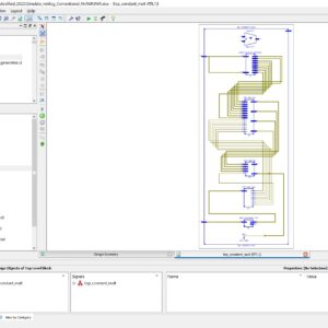
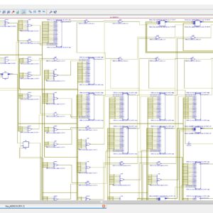
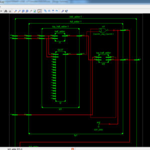
Source : DSCH3/MICROWIND
Abstract:
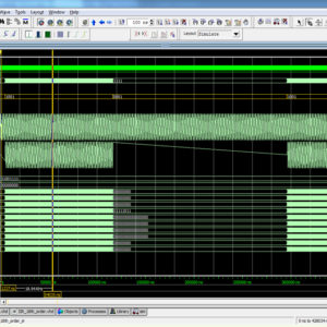
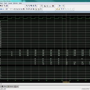
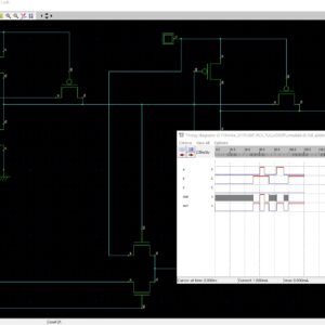
In this paper, we are proposed a level converting retention flip-flop for Zigbee Soc, it will be using to allows the voltage regulator that generates the core supply voltage (VDD, core), to be turned off in the standby mode, and it thus reduces the standby power of the Zigbee Soc. Here the Level up conversion form VDD core is achieved by and embedded nMOS pass transistor level-conversion scheme that uses a low only signal transmitting technique. By embedding a retention latch and level-up converter into the data-to-output path of the proposed RFF, the RFF resolves the problems of the static RAM-based RFF, such as large dc current and low readability caused by threshold drop. The proposed RFF does not also require additional control signals for power mode transitioning. Using 0.13-μm process technology, we implemented an RFF with VDD,core and VDD,IO of 1.2 and 2.5 V, respectively. The maximum operating frequency is 300 MHz. The active energy of the RFF is 191.70 fJ, and its standby power is 350.25 pW.
List of the following materials will be included with the Downloaded Backup:
Proposed System:
Software Implementation:
Hardware Implementation:
Abstract: In information theory, a low-density parity-check (LDPC) code is a linear error correcting code, a method of transmitting a message over a noisy transmission channel. An LDPC is constructed using a sparse bipartite graph. LDPC codes are capacity-approaching codes, which means that practical constructions exist that allow the noise threshold to be set very close (or even arbitrarily close on the BEC) to the theoretical maximum (the Shannon limit) for a symmetric memory-less channel. The noise threshold defines an upper bound for the channel noise, up to which the probability of lost information can be made as small as desired. Using iterative belief propagation techniques, LDPC codes can be decoded in time linear to their block length.
List of the following materials will be included with the Downloaded Backup:This paper presents a fixed-point reconfigurable parallel VLSI hardware architecture for real-time Electrical Capacitance Tomography (ECT). Another FPGA module performs the inverse steps of the tomography algorithm. A dual port built-in memory banks store the sensitivity matrix, the actual value of the capacitances, and the actual image with RGB format. A two dimensional (2D) core multiprocessing elements (PE) engine intercommunicates with these memory banks via parallel buses. We are focus only on the FPGA module because the design is decide the power consumption and cost. The proposed architecture of this paper analysis the logic size, area and power consumption using Xilinx 14.2.
List of the following materials will be included with the Downloaded Backup:This system presents a fully pipelined color demosaicking design. To improve the quality of reconstructed images, a linear deviation compensation scheme was created to increase the correlation between the interpolated and neighboring pixels. Furthermore, immediately interpolated green color pixels are first to be used in hardware-oriented color demosaicking algorithms, which efficiently promoted the quality of the reconstructed image. A boundary detector and boundary mirror machine were added to improve the quality of pixels located in boundaries. In addition, a hardware sharing technique was used to reduce the hardware costs of three interpolators. Finally these are implemented and get the simulated result is compared to the previous architecture. The code are simulated and power, area, cost are taken using Xilinx 14.2 software and MATLAB. Compared with the previous low complexity designs, this work has the benefits in terms of low cost, low power consumption, and high performance.
List of the following materials will be included with the Downloaded Backup:
Abstract: We propose a low-power content-addressable memory (CAM) employing a new algorithm for associativity between the input tag and the corresponding address of the output data of 128bit. The proposed architecture is based on a recently developed sparse clustered network using binary connections that on-average eliminates most of the parallel comparisons performed during a search. Therefore, the dynamic energy consumption of the proposed design is significantly lower compared with that of a conventional low-power CAM design. Given an input tag, the proposed architecture computes a few possibilities for the location of the matched tag and performs the comparisons on them to locate a single valid match. A design methodology based on the silicon area and power budgets, and performance requirements is discussed. The proposed architecture of this paper will be analysis the logic size, area and power consumption using Xilinx 14.2.
List of the following materials will be included with the Downloaded Backup:
Abstract:
In this brief, a low-cost low-power all-digital spread spectrum clock generator (ADSSCG) is presented. The proposed ADSSCG can provide an accurate programmable spreading ratio with process, voltage, and temperature variations. To maintain the frequency stability while performing triangular modulation, the fast-relocked mechanism is proposed. The proposed fast-relocked ADSSCG is implemented in a standard performance 90-nm CMOS process, and the active area is 200 µm × 200 µm. The experimental results show that the electromagnetic interference reduction is 14.61 dB with a 0.5% spreading ratio and 19.69 dB with a 2% spreading ratio at 270 MHz The power consumption is 443 µW at 270 MHz with a 1.0 V power supply.
List of the following materials will be included with the Downloaded Backup:Abstract: We are briefly discussed about the 64bit parallel self timed adder based on the recursive formulation. The adder is also based on the asynchronous logic circuit and the transistor is connected in parallel. This adder is chance the path automatically, so the delay is configures automatically. The completion detection unit is given the additional support for practical implementation. The simulation is take place with 130nm CMOS technology for the adder circuit. Finally the power consumption for 64bit adder is 0.29mW.
List of the following materials will be included with the Downloaded Backup:Abstract: Interconnections are increasingly the dominant contributor to delay, area and energy consumption in CMOS digital circuits. The proposed implementation overcomes several limitations found in previous quaternary implementations published so far, such as the need for special features in the CMOS process or power-hungry current-mode cells. We have to use the 512bit quaternary Look Up Table for high level of operations in the FPGA. The proposed architecture of this paper will be planned to implemented and also analysis the output current, output voltage, area using Xilinx 14.3.
List of the following materials will be included with the Downloaded Backup:₹15,000.00 Original price was: ₹15,000.00.₹10,000.00Current price is: ₹10,000.00.
₹20,000.00 Original price was: ₹20,000.00.₹10,000.00Current price is: ₹10,000.00.
Copyright © 2024 Nxfee Innovation.
Reviews
There are no reviews yet.