Proposed Title :
A 45nm CMOS Technology Exploring low power and Fast 4 bit Full Adder using XOR/XNOR Gates
Improvement of this Project:
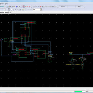
In this project we proposed 1 bit full adder using 45nm CMOS technology and compare with Existing 65nm CMOS technology.
Software implementation:
- TANNER EDA
Proposed Abstract :
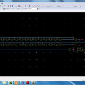
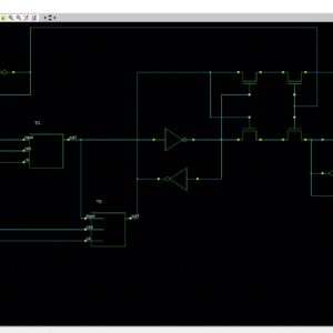
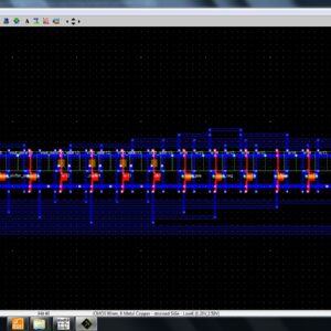
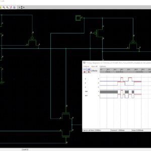
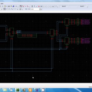
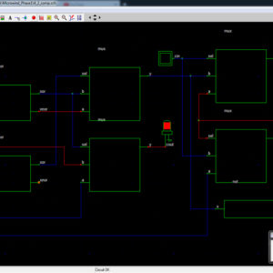
This paper, explores 4 bit full adder using XOR/XNOR or simultaneous XOR-XNOR gates and also consuming power and area of the circuit and increasing speed. This paper propose 4 bit full adder using full swing XOR/XNOR gates. The existing system simulated in 65nm CMOS technology and using hybrid 1 bit full adder. So it consumes more power for implementation. The proposed circuits simulation results based on 45nm CMOS technology model, it have superior speed and reducing area, power consumption and this circuit has high speed, low power using power delay product (PDP). In the proposed method, the numerical computation particle swarm optimization algorithm is used to achieve the desired value for optimum PDP with less iteration. In the proposed circuits new transistor sizing is implemented to optimize the PDP circuits. The proposed architecture results are compared with area, power and speed of the existing architecture.
” Thanks for Visit this project Pages – Buy It Soon “
Low-Power and Fast Full Adder by Exploring New XOR and XNOR Gates
“Buy VLSI Projects On On-Line”
Terms & Conditions:
- Customer are advice to watch the project video file output, before the payment to test the requirement, correction will be applicable.
- After payment, if any correction in the Project is accepted, but requirement changes is applicable with updated charges based upon the requirement.
- After payment the student having doubts, correction, software error, hardware errors, coding doubts are accepted.
- Online support will not be given more than 3 times.
- On first time explanations we can provide completely with video file support, other 2 we can provide doubt clarifications only.
- If any Issue on Software license / System Error we can support and rectify that within end of the day.
- Extra Charges For duplicate bill copy. Bill must be paid in full, No part payment will be accepted.
- After payment, to must send the payment receipt to our email id.
- Powered by NXFEE INNOVATION, Pondicherry.
Payment Method :
- Pay Add to Cart Method on this Page
- Deposit Cash/Cheque on our a/c.
- Pay Google Pay/Phone Pay : +91 9789443203
- Send Cheque through courier
- Visit our office directly
- Pay using Paypal : Click here to get NXFEE-PayPal link