₹20,000.00Original price was: ₹20,000.00.₹12,000.00Current price is: ₹12,000.00.
Source : Verilog HDL
Abstract:
Low-precision arithmetic operations to accelerate deep-learning applications on field-programmable gate arrays (FPGAs) have been studied extensively, because they offer the potential to save silicon area or increase throughput. However, these benefits come at the cost of a decrease in accuracy. In this article, we demonstrate that reconfigurable constant coefficient multipliers (RCCMs) offer a better alternative for saving the silicon area than utilizing low-precision arithmetic. RCCMs multiply input values by a restricted choice of coefficients using only adders, subtractors, bit shifts, and multiplexers (MUXes), meaning that they can be heavily optimized for FPGAs. We propose a family of RCCMs tailored to FPGA logic elements to ensure their efficient utilization. To minimize information loss from quantization, we then develop novel training techniques that map the possible coefficient representations of the RCCMs to neural network weight parameter distributions. This enables the usage of the RCCMs in hardware, while maintaining high accuracy. We demonstrate the benefits of these techniques using AlexNet, ResNet-18, and ResNet-50 networks. The resulting implementations achieve up to 50% resource savings over traditional 8-bit quantized networks, translating to significant speedups and power savings. Our RCCM with the lowest resource requirements exceeds 6-bit fixed point accuracy, while all other implementations with RCCMs achieve at least similar accuracy to an 8-bit uniformly quantized design, while achieving significant resource savings.
List of the following materials will be included with the Downloaded Backup:
₹25,000.00Original price was: ₹25,000.00.₹10,000.00Current price is: ₹10,000.00.
Source : Verilog HDL
Abstract:
Cryptography systems have become inseparable parts of almost every communication device. Among cryptography algorithms, public-key cryptography, and in particular elliptic curve cryptography (ECC), has become the most dominant protocol at this time. In ECC systems, polynomial multiplication is considered to be the most slow and area consuming operation. This article proposes a novel hardware architecture for efficient field-programmable gate array (FPGA) implementation of Finite field multipliers for ECC. Proposed hardware was implemented on different FPGA devices for various operand sizes, and performance parameters were determined. Comparing to state-of-the art works, the proposed method resulted in a lower combinational delay and area–delay product indicating the efficiency of design.
List of the following materials will be included with the Downloaded Backup:
₹16,000.00Original price was: ₹16,000.00.₹10,000.00Current price is: ₹10,000.00.
Source : Verilog HDL
Abstract:
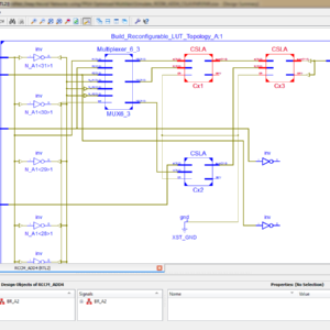
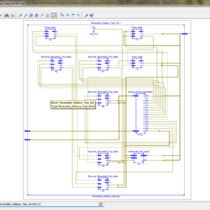
Today, reversible logic can be used for designing low-power CMOS circuits, optical data processing, DNA computations, biological researches, quantum circuits and nanotechnology. Sometimes using of reversible logic is inevitable such as build quantum computers. Reversible logic circuits structure is much more complicated than irreversible logic circuits. Multiplication operation is considered as one of the most important operations in the ALU unit. In this paper, we have proposed two 4×4 reversible unsigned multiplier circuits in which Wallace tree method is used to reduce the depth of circuits. In first design, the partial products circuit is designed using TG and FG gates so that TG is used to produce the partial products and FG for fan-out. In the second design, TG and PG gates are used to produce the partial products and no fan-out is required. Moreover, we have used PG gate and Feynman' block as reversible half-adder (HA) and full-adder (FA) in the summation network, respectively. In the first design, the main purpose is to decrease the depth of the circuit and increase the circuit speed. In the second design we would attempt to improve quantum parameters the number of garbage outputs, constant inputs and quantum cost. The evaluation results show that the first design, in terms of delay, is the fastest circuit. Also, the second design in terms of the number of constant inputs, garbage outputs and quantum cost is better than other designs.
List of the following materials will be included with the Downloaded Backup:
₹32,000.00Original price was: ₹32,000.00.₹12,000.00Current price is: ₹12,000.00.
Source : Verilog HDL
Base Paper Abstract:
High speed multimedia applications have paved way for a whole new area in high speed error-tolerant circuits with approximate computing. These applications deliver high performance at the cost of reduction in accuracy. Furthermore, such implementations reduce the complexity of the system architecture, delay and power consumption. This paper explores and proposes the design and analysis of two approximate compressors with reduced area, delay and power with comparable accuracy when compared with the existing architectures. The proposed designs are implemented using 45 nm CMOS technology and efficiency of the proposed designs have been extensively verified and projected on scales of area, delay, power, Power Delay Product (PDP), Error Rate (ER), Error Distance (ED), and Accurate Output Count (AOC). The proposed approximate 4 : 2 compressor shows 56.80% reduction in area, 57.20% reduction in power, and 73.30% reduction in delay compared to an accurate 4 : 2 compressor. The proposed compressors are utilised to implement 8 × 8 and 16 × 16 Dadda multipliers. These multipliers have comparable accuracy when compared with state-of-the-art approximate multipliers. The analysis is further extended to project the application of the proposed design in error resilient applications like image smoothing and multiplication.
List of the following materials will be included with the Downloaded Backup:
₹35,000.00Original price was: ₹35,000.00.₹14,000.00Current price is: ₹14,000.00.
Source : Verilog HDL
Abstract:
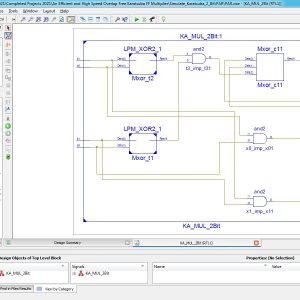
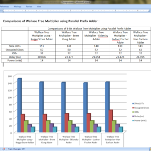
Major operation block in any processing unit is a multiplier. There are many multiplication algorithms are proposed, by using which multiplier structure can be designed. Among various multiplication algorithms, Wallace tree multiplication algorithm is beneficial in terms of speed of operation. With the advancement of technology, demand for circuits with high speed and low area is increasing. In order to improve the speed of Wallace tree multiplier without degrading its area parameter, a new structure of Wallace tree multiplier is proposed in this paper. In the proposed structure, the final addition stage of partial products is performed by parallel prefix adders (PPAs). In this paper, five Wallace tree multiplier structures are proposed using Kogge stone adder, Sklansky adder, Brent Kung adder, Ladner Fischer adder and Han carlson adder. All the multiplier structures are designed using Verilog HDL in Xilinix 13.2 design suite. The proposed structures are simulated using ISIM simulator and synthesized using XST synthesizer. The proposed designs are analyzed with respect to traditional multiplier design in terms of area (No. of LUTs) and delay (ns).
List of the following materials will be included with the Downloaded Backup:
₹16,000.00Original price was: ₹16,000.00.₹8,000.00Current price is: ₹8,000.00.
Source : Verilog HDL
Base Paper Abstract:
This letter presents a novel hardware-efficient approximate 4-2 compressor design that significantly enhances accuracy through a systematic analysis of input patterns obtained from practical applications. We incorporate a majority operation and a compound gate in the compressor design to effectively boost hardware efficiency in multiplications. Our design approach results in substantial error reductions, with normalized mean error distance (NMED) and mean relative error distance (MRED) decreasing by up to 74.84% and 82.04%, respectively, compared to existing approximate multipliers discussed in this letter. When implemented in a 32-nm CMOS technology, the approximate multiplier adopting the proposed 4-2 compressor achieves excellent hardware efficiency, reducing area, power, and energy consumption by up to 8.95%, 13.02%, and 13.02%, respectively, compared to the other alternatives. Moreover, our design delivers enhanced performance in image processing tasks, achieving up to a 4.84× increase in peak signal-to-noise ratio (PSNR) compared to other designs, all while optimizing hardware efficiency. Index Terms—Approximate multiplier, majority operation, compound gate, image processing, approximate 4-2 compressor.
List of the following materials will be included with the Downloaded Backup:
₹12,000.00Original price was: ₹12,000.00.₹8,000.00Current price is: ₹8,000.00.
Source : Verilog HDL
Base Paper Abstract:
In this article, a framework for the analog implementation of a deep convolutional neural network (CNN) is introduced and used to derive a new circuit architecture which is composed of an improved analog multiplier and circuit blocks implementing the ReLU activation function and the argmax operator. The operating principles of the individual blocks, as well as those of the complete architecture, are analysed and used to realize a low-power analog classifier, consuming less than 1.8 µW. The proper operation of the classifier is verified via a comparison with a software equivalent implementation and its performance is evaluated against existing circuit architectures. The proposed architecture is implemented in a TSMC 90-nm CMOS process and simulated using Cadence IC Suite for both schematic and layout design. Corner and Monte Carlo mismatch simulations of the schematic and the physical circuit (post layout) were conducted to evaluate the effect of transistor mismatches and process voltage temperature (PVT) variations and to showcase a proposed systematic method for offsetting their effect.
List of the following materials will be included with the Downloaded Backup:
₹25,000.00Original price was: ₹25,000.00.₹10,000.00Current price is: ₹10,000.00.
Source : Verilog HDL
Base Paper Abstract:
Due to their shrinking feature sizes as well as environmental influences, such as high-energy radiation, electrical noise, and particle strikes, integrated circuits are getting more vulnerable to transient faults. Accordingly, how to make those circuits more robust has become an essential step in today’s design flows. Methods increasing the robustness of circuits against these faults already exist for a long period of time but either introduce huge additional logic, change the timing behavior of the circuit, or are applicable for dedicated circuits such as microprocessors only. In this paper, we propose an alternative method, which overcomes these drawbacks by determining application specific knowledge of the circuit, namely the relations of flip-flops and when they assume the same value. By this, we exploit partial redundancies, which are inherent in most circuits anyway (even the optimized ones), to frequently compare the circuit signals for their correctness—eventually leading to an increased robustness. Since determining the correspondingly needed information is a computationally hard task, formal methods, such as bounded model checking, satisfiability-based automatic test pattern generation, and binary decision diagrams, are utilized for this purpose. The resulting methodology requires only a slight increase in additional hardware, does only influence the timing behavior of the circuit negligibly, and is automatically applicable to arbitrary circuits. Experimental evaluations confirm these benefits.
List of the following materials will be included with the Downloaded Backup:
₹16,000.00Original price was: ₹16,000.00.₹12,000.00Current price is: ₹12,000.00.
Source : Verilog HDL
Proposed Abstract:
Multiplication is a critical operation in many digital signal processing and machine learning applications, where fast and efficient computation is essential. However, conventional multipliers that compute n x n bit products result in significant hardware overhead and increased power consumption. To address these challenges, this paper proposes an FPGA implementation of an 8x8 truncated multiplier utilizing the Brent-Kung parallel prefix adder to improve both speed and resource efficiency. The proposed truncated multiplier limits the output to n bits, discarding the least significant bits and utilizing a variable correction technique to minimize the error introduced by truncation. By selectively summing the most significant columns, the design achieves a balance between accuracy and hardware efficiency, providing a reduced-area solution for approximate computing. The Brent-Kung parallel prefix adder is integrated into the multiplier architecture to optimize the carry propagation stage, reducing the overall critical path delay. This adder is known for its logarithmic depth, which significantly improves the speed of the summation process while using fewer logic gates compared to traditional adders. This design was implemented in Verilog HDL and synthesized on a Xilinx Virtex-5 FPGA platform. Comparative analysis with a conventional multiplier shows that the proposed truncated multiplier achieves a notable reduction in FPGA resource utilization, including logic elements and power consumption, without sacrificing significant accuracy. The architecture particularly suitable for applications where speed and low power consumption are paramount, such as real-time image processing, DSP systems, and machine learning accelerators.
List of the following materials will be included with the Downloaded Backup:
₹25,000.00Original price was: ₹25,000.00.₹10,000.00Current price is: ₹10,000.00.
Source : Verilog HDL
Base Paper Abstract:
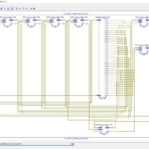
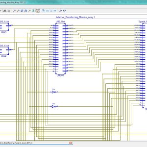
With the rise of 5G networks and the increasing number of communication devices, improving communication quality is essential. One approach is adaptive digital beamforming, which adjusts an antenna array’s radiation pattern based on the desired received signal. Adaptation based on Least-Mean Squared (LMS) and its variants is still one of the most common literature methods. Although LMS techniques present good computational performance, the increase in antennas’ numbers led to high-performance hardware. Platforms such as Field Programmable Gate Arrays (FPGAs), designed for massive array systems, enables high-performance energy-efficient architectures. This work proposes a parallel implementation of a massive array beamforming composed of a spatial filter and adaptation unit based on LMS on FPGA. The proposed design presents ten times fewer hardware requirements and 30 times less power consumption than state of the art.
List of the following materials will be included with the Downloaded Backup:
₹20,000.00Original price was: ₹20,000.00.₹10,000.00Current price is: ₹10,000.00.
Source : Verilog HDL
Abstract:
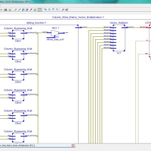
This article presents a reconfigurable accelerator for Recurrent Neural networks with fine-grained Column Wise matrix–vector multiplication (RENOWN). We propose a novel latency-hiding architecture for recurrent neural network (RNN) acceleration using column-wise matrix–vector multiplication (MVM) instead of the state-of-the-art row-wise operation. This hardware (HW) architecture can eliminate data dependencies to improve the throughput of RNN inference systems. Besides, we introduce a configurable checkerboard tiling strategy which allows large weight matrices, while incorporating various configurations of element-based parallelism (EP) and vector-based parallelism (VP). These optimizations improve the exploitation of parallelism to increase HW utilization and enhance system throughput. Evaluation results show that our design can achieve over 29.6 tera operations per second (TOPS) which would be among the highest for field-programmable gate array (FPGA)-based RNN designs. Compared to state-of-the-art accelerators on FPGAs, our design achieves 3.7–14.8 times better performance and has the highest HW utilization.
List of the following materials will be included with the Downloaded Backup:
We can provide Online Support Wordlwide, with proper execution, explanation and additionally provide explanation video file for execution and explanations.
24/7 Support Center
NXFEE, will Provide on 24x7 Online Support, You can call or text at +91 9789443203, or email us nxfee.innovation@gmail.com
Terms & Conditions:
Customer are advice to watch the project video file output, and before the payment to test the requirement, correction will be applicable.
After payment, if any correction in the Project is accepted, but requirement changes is applicable with updated charges based upon the requirement.
After payment the student having doubts, correction, software error, hardware errors, coding doubts are accepted.
Online support will not be given more than 3 times.
On first time explanation we can provide completely with video file support, other 2 we can provide doubt clarifications only.
If any Issue on Software license / System Error we can support and rectify that within end of day.
Extra Charges For duplicate bill copy. Bill must be paid in full, No part payment will be accepted.
After payment, to must send the payment receipt to our email id.
Powered by NXFEE INNOVATION, Pondicherry.
Call us today at : +91 9789443203 or Email us at nxfee.innovation@gmail.com