Proposed Title :
FPGA Implementation of M-PSK Modulation and Demodulation of 4, 8, 16-QPSK
Improvement of this Project:
- Updated with 4-QPSK, 8-QPSK, 16-QPSK Modulaiton and Demodulation
Software implementation:
- Modelsim
- Xilinx 14.2
Proposed System:
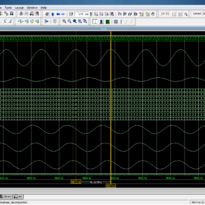
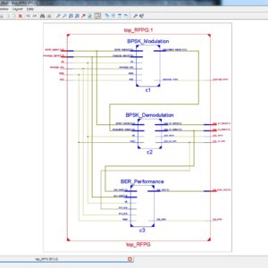
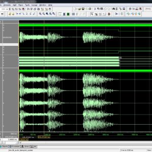
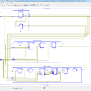
In the Proposed system of PSK Modulation and Demodulation will integrated with 4PSK, 8PSK and 16PSK in single architecture, with reduced the High complexity and reduced power consumption. Here, the input data to be transferred as a Image file, this image will loaded into MATLAB to convert Image to hex conversion, these hex file data will written into Memory with help of Test bench, and transferred after filling the image data. Once data is started, it will process on LSB Shifting of data byte based configuration will decide quadrant phase shifting of sine and cosine signals in modulation scheme. In demodulation scheme, to receive quadrant modulation and analysis sine and cosine signal phase shifting, using demodulator oscillator and provide a output data. Finally the design will tested with fading channel based noise generation with BER Testing.
” Thanks for Visit this project Pages – Buy It Soon “
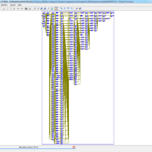
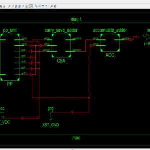
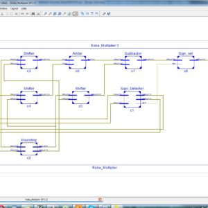
High Performance VLSI architecture for M-PSK modems
“Buy VLSI Projects On On-Line”
Terms & Conditions:
- Customer are advice to watch the project video file output, before the payment to test the requirement, correction will be applicable.
- After payment, if any correction in the Project is accepted, but requirement changes is applicable with updated charges based upon the requirement.
- After payment the student having doubts, correction, software error, hardware errors, coding doubts are accepted.
- Online support will not be given more than 3 times.
- On first time explanations we can provide completely with video file support, other 2 we can provide doubt clarifications only.
- If any Issue on Software license / System Error we can support and rectify that within end of the day.
- Extra Charges For duplicate bill copy. Bill must be paid in full, No part payment will be accepted.
- After payment, to must send the payment receipt to our email id.
- Powered by NXFEE INNOVATION, Pondicherry.
Payment Method :
- Pay Add to Cart Method on this Page
- Deposit Cash/Cheque on our a/c.
- Pay Google Pay/Phone Pay : +91 9789443203
- Send Cheque through courier
- Visit our office directly
- Pay using Paypal : Click here to get NXFEE-PayPal link