9789443203
nxfee.innovation@gmail.com
Facebook Youtube Linkedin
  • VLSI PHD Research
  • *** Buy VLSI Research Projects ***
  • Freelance
  • Contact
  • VLSI Mini Projects
  • Archives
  • NXFEE Youtube Channel
What are you looking for?
Trending Searches: Low Power VLSI High Speed VLSI Signal Processing Image Processing
Popular categories
2014

2014

11 products
2015

2015

39 products
2016

2016

30 products
2017

2017

16 products
2018

2018

17 products
2019

2019

42 products
View all categories
My Account

Lost password?

0 0
0 Shopping Cart
Shopping cart (0)
Subtotal: ₹0.00

Checkout

REFER YOUR FRIENDS WHO WILL NEED VLSI PROJECTS
“EARN Rs.1,000/- FOR ONE VLSI PROJECT” ( Amount will given After Registration )
Menu Categories
  • VLSI PHD Research
  • *** Buy VLSI Research Projects ***
  • Freelance
  • Contact
  • VLSI Mini Projects
  • Archives
  • NXFEE Youtube Channel
  • 2015
  • 2020
  • Low power VLSI Design
  • 2021
  • Image Processing
  • 2022
  • 2016
  • VLSI 2023
  • High speed VLSI Design
  • VLSI_2023
  • Accessories
  • IEEE
  • VLSI Application / Interface and Mini Projects
  • VLSI
  • VLSI 2024
  • NOC VLSI Design
  • VLSI 2025
  • 2017
  • 2014
  • 2018
  • Area Efficient
  • 2019
Cart 0
0 0
0 Shopping Cart
Shopping cart (0)
Subtotal: ₹0.00

Checkout

REFER YOUR FRIENDS WHO WILL NEED VLSI PROJECTS
“EARN Rs.1,000/- FOR ONE VLSI PROJECT” ( Amount will given After Registration )
Home Shop

VLSI_2023

Return to previous page

IEEE Transactions on VLSI 2023

Following Novelty based Research Projects not yet Published in Any Journal 

Customization Available for Journal Publications

Grid
List
Show
sale OFFER 28%
Myocardial_Infarction
Quick View Add to cart
High speed VLSI Design, VLSI, VLSI 2023, VLSI_2023

MInSC: A VLSI Architecture for Myocardial Infarction Stages Classifier for Wearable Healthcare Applications

₹25,000.00 Original price was: ₹25,000.00.₹18,000.00Current price is: ₹18,000.00.
Source : Verilog HDL

Base Paper Abstract:

Myocardial Infarction (MI) is a critical heart abnormality causing millions of fatalities worldwide every year. MI progress in three stages based on its severity causing several changes in an Electrocardiogram (ECG) signal. It is very critical to capture these variations, which requires continuous monitoring of the ECG signal of the patient. Therefore, it becomes imperative to develop a low power VLSI architecture to address the prognosis of MI. In this brief, for the first time, an area and power efficient design of a five stage classifier is proposed, which detects the progression of various stages of MI using ECG beats in real time. The proposed architecture has an area and total power utilization of 1.38mm2 and 5.12µW, respectively at SCL 180nm Bulk CMOS technology. The low power and area requirements and multiclass classification capability of the proposed design make it suitable to be used in wearable devices.

List of the following  materials will be included with the Downloaded Backup:
1. Source code ( Modelsim/ Xilinx/ Quartus/ DSCH3/ Microwind)
2. Existing and Proposed Project Comparison with output video 
3. Basic Documentation (20 to 30 Pages):
3.1 Proposed Title
3.2 Proposed Abstract
3.3 Advantages & Disadvantages
3.4 Improvement of this Project
3.5 Existing System with Notes
3.6 Proposed System with Notes
3.7 Literature Survey
3.8 Software Related Notes
3.9 VLSI and HDL Language / Tanner Notes
3.10 References & Reference Paper for More Pages
4. Online Support ( Any Desk / Zoom / Google Meet)
 
sale OFFER 47%
Vedic Multiplier
Quick View Add to cart
Area Efficient, VLSI, VLSI 2023, VLSI_2023

Design of High Speed 8-bit Vedic Multiplier using Brent Kung Parallel Prefix Adder

₹15,000.00 Original price was: ₹15,000.00.₹8,000.00Current price is: ₹8,000.00.
Source : Verilog HDL

Base Paper Abstract:

One of the primary purposes of a digital signal processing system is multiplication. The multiplier’s performance affects the DSP system’s overall performance. Therefore, it is crucial to create an effective and quick multiplier implementation design. Vedic mathematics can be used to simplify complex computations so that they are easier to perform verbally. Urdhva Triyambakam is the multiplication algorithm used in Vedic math. In this paper, we employing Brent Kung adder to enhance the Vedic multiplier’s performance. The Urdhva Tiryagbhyam sutra is being used in place of other multiplication strategies since it applies to all instances of algorithms for N x N bit numbers and produces the least amount of latency. Four 4-bit vedic multipliers, two 8-bit Brent Kung adders, one 4-bit Brent Kung adder, and an OR gate are used to create an 8-bit vedic multiplier. A 4-bit vedic multiplier is created similarly by combining four 2-bit vedic multipliers, two 4-bit Brent Kung Adders, one 2-bit Brent Kung Adder, and one OR gate. These four-bit vedic multipliers are then combined to form an eight-bit vedic multiplier. After that, Xilinx Vivado Software is used to simulate and synthesis the 8 x 8 Vedic Multiplier, which was coded in Verilog HDL. The proposed Vedic Multiplier is outperformed in terms of speed when compared to related works.

List of the following  materials will be included with the Downloaded Backup:
1. Source code ( Modelsim/ Xilinx/ Quartus/ DSCH3/ Microwind)
2. Existing and Proposed Project Comparison with output video 
3. Basic Documentation (20 to 30 Pages):
3.1 Proposed Title
3.2 Proposed Abstract
3.3 Advantages & Disadvantages
3.4 Improvement of this Project
3.5 Existing System with Notes
3.6 Proposed System with Notes
3.7 Literature Survey
3.8 Software Related Notes
3.9 VLSI and HDL Language / Tanner Notes
3.10 References & Reference Paper for More Pages
4. Online Support ( Any Desk / Zoom / Google Meet)
 
sale OFFER 47%
Approximate Wallace Tree Multiplier
Quick View Add to cart
Area Efficient, VLSI, VLSI 2023, VLSI_2023

Design and Implementation of an 8-bit Approximate Wallace Tree Multiplier for Energy Efficient Deep Neural Networks

₹15,000.00 Original price was: ₹15,000.00.₹8,000.00Current price is: ₹8,000.00.
Source : Verilog HDL

Base Paper Abstract:

Approximate arithmetic computing circuits and architectures have been proven to be energy efficient designs for Deep Neural Networks (DNNs) which are error resilient. In this paper, an approximate 8-bit Wallace Multiplier has been proposed and designed in 90nm CMOS technology for energy efficiency. The proposed 8-bit approximate multiplier design consumes ~32% less energy in comparison to an accurate 8-bit Wallace Tree multiplier with less than 20% Mean Relative Error (MRE).

List of the following  materials will be included with the Downloaded Backup:
1. Source code ( Modelsim/ Xilinx/ Quartus/ DSCH3/ Microwind)
2. Existing and Proposed Project Comparison with output video 
3. Basic Documentation (20 to 30 Pages):
3.1 Proposed Title
3.2 Proposed Abstract
3.3 Advantages & Disadvantages
3.4 Improvement of this Project
3.5 Existing System with Notes
3.6 Proposed System with Notes
3.7 Literature Survey
3.8 Software Related Notes
3.9 VLSI and HDL Language / Tanner Notes
3.10 References & Reference Paper for More Pages
4. Online Support ( Any Desk / Zoom / Google Meet)
 
sale OFFER 47%
Conventional Shift &Add Multiplier
Quick View Add to cart
Area Efficient, VLSI, VLSI 2023, VLSI_2023

An Optimization in Conventional Shift &Add Multiplier for Area-Efficient Implementation on FPGA

₹15,000.00 Original price was: ₹15,000.00.₹8,000.00Current price is: ₹8,000.00.
Source : Verilog HDL

Base Paper Abstract:

FPGA is familiar with prototyping and implementing simple to complex DSP systems. The FPGA based design may be highly affected by factors that include selection of an FPGA board, Electronic Design Automation Tool and the Programming Techniques to optimize the algorithm. The algorithm optimization results in a more compact design regarding the area and achieved frequency. In DSP algorithms optimization, the major bottleneck is the multiplier complexity evident in, for example - FIR, IIR, FFT, and others. Research shows much work on multiplier optimization. Despite all possible optimization techniques, the multiplier consumes tremendous resources when translated on hardware, with more power consumption and observed delay. The proposed work is novel in that it brings resources optimization in a familiar shift and add multiplier algorithm by implementing the design in FPGA and comparing the results with the existing shift, and add a multiplier. In the implementation of the design, Xilinx Vertex -7 FPGA is used along with ISE 14.2 simulators. The parameters to compare are the Lookup tables (Logic element of FPGA), adder/subtractors and the multiplexers, along with performance characters, like the operating frequency, delay and total levels of logic (path travelled by the signal in register transfer level). The output shows that the anticipated design is an excellent alternative to the conventional shift and add algorithm.

List of the following  materials will be included with the Downloaded Backup:
1. Source code ( Modelsim/ Xilinx/ Quartus/ DSCH3/ Microwind)
2. Existing and Proposed Project Comparison with output video 
3. Basic Documentation (20 to 30 Pages):
3.1 Proposed Title
3.2 Proposed Abstract
3.3 Advantages & Disadvantages
3.4 Improvement of this Project
3.5 Existing System with Notes
3.6 Proposed System with Notes
3.7 Literature Survey
3.8 Software Related Notes
3.9 VLSI and HDL Language / Tanner Notes
3.10 References & Reference Paper for More Pages
4. Online Support ( Any Desk / Zoom / Google Meet)
 
sale OFFER 35%
Image_Encryption
Quick View Add to cart
Image Processing, VLSI, VLSI 2023, VLSI_2023

An Efficient Image Encryption Algorithm Based on Innovative DES Structure and Hyperchaotic Keys

₹85,000.00 Original price was: ₹85,000.00.₹55,000.00Current price is: ₹55,000.00.
Source : Verilog HDL

Base Paper Abstract:

In fact, as a traditional encryption method, DES has been certified as an unsuitable tool for ciphering due to its smaller key space. Further, in concern of the real-time encryption in the current fast communication era, such as 5G, long-time as well as large computational level processes are not gotten into the consideration. As a result, an innovative encryption structure with hyperchaotic keys for efficient encryption is constructed, where the frame of DES structure is applied, the plain image is shuffled through row and column directions in the first round, and then rearranged to be 64 blocks to fit into the frame of DES structure for 4 rounds ciphering with hyperchaotic subkeys. Also, in order to encrypt the content of the image at the block level, a set of alternative S-box has been produced in this article as well. The simulation results indicate that the proposed scheme is feasible and reliable for digital image encrypting, not only a large key space can be obtained, but also the low correlation of the adjacent contents can be achieved, and further, in comparison of several existing approaches, less-computational resource can be proven as well. In particular, due to the innovative DES structure, the computational speed is significantly faster than the original DES algorithm and many other chaos-based image ciphering schemes.

List of the following  materials will be included with the Downloaded Backup:
1. Source code ( Modelsim/ Xilinx/ Quartus/ DSCH3/ Microwind)
2. Existing and Proposed Project Comparison with output video 
3. Basic Documentation (20 to 30 Pages):
3.1 Proposed Title
3.2 Proposed Abstract
3.3 Advantages & Disadvantages
3.4 Improvement of this Project
3.5 Existing System with Notes
3.6 Proposed System with Notes
3.7 Literature Survey
3.8 Software Related Notes
3.9 VLSI and HDL Language / Tanner Notes
3.10 References & Reference Paper for More Pages
4. Online Support ( Any Desk / Zoom / Google Meet)
 
sale OFFER 38%
Multiple Constant Multiplication at Minimal Hardware Cost
Quick View Add to cart
Area Efficient, VLSI, VLSI 2023, VLSI_2023

Toward the Multiple Constant Multiplication at Minimal Hardware Cost

₹16,000.00 Original price was: ₹16,000.00.₹10,000.00Current price is: ₹10,000.00.
Source : Verilog HDL

Base Paper Abstract:

Multiple Constant Multiplication (MCM) over integers is a frequent operation arising in embedded systems that require highly optimized hardware. An efficient way is to replace costly generic multiplication by bit-shifts and additions, i. e. a multiplier less circuit. In this work, we improve the state of-the-art optimal approach for MCM, based on Integer Linear Programming (ILP). We introduce a new low-level hardware cost metric, which counts the number of one-bit adders and demonstrate that it is strongly correlated with the LUT count. This new model permitted us to consider intermediate truncations that permit to significantly save resources when a full output precision is not required. We incorporate the error propagation rules into our ILP model to guarantee a user-given error bound on the MCM results. The proposed ILP models for multiple flavors of MCM are implemented as an open-source tool and, combined with an automatic code generator, provide a complete coefficient-to-VHDL flow. We evaluate our models in extensive experiments, and propose an in-depth analysis of the impact that design metrics have on synthesized hardware.

List of the following  materials will be included with the Downloaded Backup:
1. Source code ( Modelsim/ Xilinx/ Quartus/ DSCH3/ Microwind)
2. Existing and Proposed Project Comparison with output video 
3. Basic Documentation (20 to 30 Pages):
3.1 Proposed Title
3.2 Proposed Abstract
3.3 Advantages & Disadvantages
3.4 Improvement of this Project
3.5 Existing System with Notes
3.6 Proposed System with Notes
3.7 Literature Survey
3.8 Software Related Notes
3.9 VLSI and HDL Language / Tanner Notes
3.10 References & Reference Paper for More Pages
4. Online Support ( Any Desk / Zoom / Google Meet)
 
sale OFFER 36%
Digital FIR Filters
Quick View Add to cart
Low power VLSI Design, VLSI, VLSI 2023, VLSI_2023

Hybrid Protection of Digital FIR Filters

₹25,000.00 Original price was: ₹25,000.00.₹16,000.00Current price is: ₹16,000.00.
Source : Verilog HDL

Base Paper Abstract:

A digital finite impulse response (FIR) filter is a ubiquitous block in digital signal processing applications and its behavior is determined by its coefficients. To protect filter coefficients from an adversary, efficient obfuscation techniques have been proposed, either by hiding them behind decoys or replacing them by key bits. In this article, we initially introduce a query attack that can discover the secret key of such obfuscated FIR filters, which could not be broken by the existing prominent attacks. Then, we propose a first of its kind hybrid technique, including both hardware obfuscation and logic locking using a point function for the protection of parallel direct and transposed forms of digital FIR filters. Experimental results show that the hybrid protection technique can lead to FIR filters with higher security while maintaining the hardware complexity competitive or superior to those locked by prominent logic locking methods. It is also shown that the protected multiplier blocks and FIR filters are resilient to existing attacks. The results on different forms and realizations of FIR filters show that the parallel direct form FIR filter has a promising potential for a secure design.

List of the following  materials will be included with the Downloaded Backup:
1. Source code ( Modelsim/ Xilinx/ Quartus/ DSCH3/ Microwind)
2. Existing and Proposed Project Comparison with output video 
3. Basic Documentation (20 to 30 Pages):
3.1 Proposed Title
3.2 Proposed Abstract
3.3 Advantages & Disadvantages
3.4 Improvement of this Project
3.5 Existing System with Notes
3.6 Proposed System with Notes
3.7 Literature Survey
3.8 Software Related Notes
3.9 VLSI and HDL Language / Tanner Notes
3.10 References & Reference Paper for More Pages
4. Online Support ( Any Desk / Zoom / Google Meet)
 
sale OFFER 50%
Lightweight True Random Number Generator
Quick View Add to cart
Low power VLSI Design, VLSI, VLSI 2023, VLSI_2023

A Lightweight True Random Number Generator for Root of Trust Applications

₹16,000.00 Original price was: ₹16,000.00.₹8,000.00Current price is: ₹8,000.00.
Source : Verilog HDL

Base Paper Abstract:

There are many schemes proposed to protect integrated circuits (ICs) against an unauthorized access and usage, or at least to mitigate security risks. They lay foundations for hardware roots of trust whose crucial security primitives are generators of truly random numbers. In particular, such generators are used to yield one-time challenges (nonces) supporting the IC authentication protocols employed to counteract potential threats such as untrusted users accessing ICs. However, IC vendors raise several concerns regarding the complexity of these solutions, both in terms of area overhead, the impact on the design flow, and testability. These concerns have motivated this work presenting a simple, yet effective, all-digital lightweight and self-testable random number generator to produce a nonce. It builds on a generic ring generator architecture, i.e., an area and time optimized version of a linear feedback shift register, driven by a multiple-output ring oscillator. A comprehensive evaluation, based on three statistical test suits from NIST and BSI, show feasibility and efficiency of the proposed scheme and are reported herein.

List of the following  materials will be included with the Downloaded Backup:
1. Source code ( Modelsim/ Xilinx/ Quartus/ DSCH3/ Microwind)
2. Existing and Proposed Project Comparison with output video 
3. Basic Documentation (20 to 30 Pages):
3.1 Proposed Title
3.2 Proposed Abstract
3.3 Advantages & Disadvantages
3.4 Improvement of this Project
3.5 Existing System with Notes
3.6 Proposed System with Notes
3.7 Literature Survey
3.8 Software Related Notes
3.9 VLSI and HDL Language / Tanner Notes
3.10 References & Reference Paper for More Pages
4. Online Support ( Any Desk / Zoom / Google Meet)
 
sale OFFER 40%
Multipath Fully Differential OTA
Quick View Add to cart
Low power VLSI Design, VLSI, VLSI 2023, VLSI_2023

Implementation of a Multipath Fully Differential OTA in 0.18-μm CMOS Process

₹10,000.00 Original price was: ₹10,000.00.₹6,000.00Current price is: ₹6,000.00.
Source : Tanner EDA

Base Paper Abstract:

This brief implements a highly efficient fully differential trans conductance amplifier, based on several input-to-output paths. Some traditional techniques, such as positive feedback, nonlinear tail current sources, and current mirror-based paths, are combined to increase the trans conductance, thus leading to larger dc gain and higher gain bandwidth (GBW) product. Two flipped voltage-follower (FVF) cells are employed as variable current sources to provide class-AB operation and adaptive biasing of all other drivers. The proposed structure includes several input-to-output paths that play the role of dynamic current boosters during the slewing phase, thus improving the slew rate (SR) performance. The circuit was fabricated in a TSMC 0.18-µm CMOS process with a silicon area of 54.5 × 30.1 µm. Experimental results show a GBW of 173.3 MHz, a dc gain of 72.7 dB, and an SR of 139.4 V/µs for a capacitive load of 2 × 5 pF. The proposed circuit consumes 619 µW of power, under a supply voltage of 1.8 V.

List of the following  materials will be included with the Downloaded Backup:
1. Source code ( Modelsim/ Xilinx/ Quartus/ DSCH3/ Microwind)
2. Existing and Proposed Project Comparison with output video 
3. Basic Documentation (20 to 30 Pages):
3.1 Proposed Title
3.2 Proposed Abstract
3.3 Advantages & Disadvantages
3.4 Improvement of this Project
3.5 Existing System with Notes
3.6 Proposed System with Notes
3.7 Literature Survey
3.8 Software Related Notes
3.9 VLSI and HDL Language / Tanner Notes
3.10 References & Reference Paper for More Pages
4. Online Support ( Any Desk / Zoom / Google Meet)
 
sale OFFER 52%
Scalable Adaptive Filters
Quick View Add to cart
High speed VLSI Design, VLSI, VLSI 2023, VLSI_2023

ReAdapt: A Reconfigurable Datapath for Runtime Energy-Quality Scalable Adaptive Filters

₹25,000.00 Original price was: ₹25,000.00.₹12,000.00Current price is: ₹12,000.00.
Source : Verilog HDL

Base Paper Abstract:

This paper proposes ReAdapt–a reconfigurable datapath architecture for scaling the energy-quality trade-off of adaptive filtering at runtime. The ReAdapt can dynamically select four adaptive filtering algorithms for gradating complexity levels during runtime by reconfiguring the processing flow in its datapath and by blocking the switching activity (e.g., reducing the CMOS dynamic power) of unused modules with data-gating. The ReAdapt proposal can scale the energy-quality trade-off by choosing the following four different levels of filter algorithms complexity: 1) least mean square (LMS); 2) partial update normalized LMS (PU-NLMS); 3) set-membership normalized LMS (SM-NLMS); 4) normalized LMS (NLMS). The ReAdapt architecture reuses common modules of each adaptive filter, resulting in a compact VLSI hardware implementation. The ReAdapt architecture operation is implemented in a case-study for interference mitigation for electroencephalogram (EEG) signal processing. The hardware synthesis results show an increase of 6.80 times in throughput and at least a reduction of 2.84 times in energy per operation compared with the state-of-the-art adaptive filters. This paper also investigates the benefits of dynamically reconfiguring the four ReAdapt operating modes at runtime for different levels of signal-to-noise ratio (SNR) for the processed signals. We also demonstrate that dynamically reconfiguring the ReAdapt operating modes during runtime results in an optimal energy-quality trade-off which is advantageous over the conventional single static mode.

List of the following  materials will be included with the Downloaded Backup:
1. Source code ( Modelsim/ Xilinx/ Quartus/ DSCH3/ Microwind)
2. Existing and Proposed Project Comparison with output video 
3. Basic Documentation (20 to 30 Pages):
3.1 Proposed Title
3.2 Proposed Abstract
3.3 Advantages & Disadvantages
3.4 Improvement of this Project
3.5 Existing System with Notes
3.6 Proposed System with Notes
3.7 Literature Survey
3.8 Software Related Notes
3.9 VLSI and HDL Language / Tanner Notes
3.10 References & Reference Paper for More Pages
4. Online Support ( Any Desk / Zoom / Google Meet)
 
sale OFFER 40%
EEG_Approximate_Computing
Quick View Add to cart
Area Efficient, VLSI, VLSI 2023, VLSI_2023

Two Efficient Approximate Unsigned Multipliers by Developing New Configuration for Approximate 4:2 Compressors

₹20,000.00 Original price was: ₹20,000.00.₹12,000.00Current price is: ₹12,000.00.
Source : Verilog HDL

Base Paper Abstract:

Approximate computing is a promising approach for reducing power consumption and design complexity in applications that accuracy is not a crucial factor. Approximate multipliers are commonly used in error-tolerant applications. This paper presents three approximate 4:2 compressors and two approximate multiplier designs, aiming at reducing the area and power consumption, while maintaining acceptable accuracy. The paper seeks to develop approximate compressors that align positive and negative approximations for input patterns that have the same probability. Additionally, the proposed compressors are utilized to construct approximate multipliers for different columns of partial products based on the input probabilities of the two compressors in adjacent columns. The proposed approximate multipliers are synthesized using the 28nm technology. Compared to the exact multiplier, the first proposed multiplier improves power × delay and area × power by 91% and 86%, respectively, while the second proposed multiplier improves the two parameters by 90% and 84%, respectively. The performance of the proposed approximate methods was assessed and compared with the existing methods for image multiplication, sharpening, smoothing and edge detection. Also, the performance of the proposed multipliers in the hardware implementation of the neural network was investigated, and the simulation results indicate that the proposed multipliers have appropriate accuracy in these applications.

List of the following  materials will be included with the Downloaded Backup:
1. Source code ( Modelsim/ Xilinx/ Quartus/ DSCH3/ Microwind)
2. Existing and Proposed Project Comparison with output video 
3. Basic Documentation (20 to 30 Pages):
3.1 Proposed Title
3.2 Proposed Abstract
3.3 Advantages & Disadvantages
3.4 Improvement of this Project
3.5 Existing System with Notes
3.6 Proposed System with Notes
3.7 Literature Survey
3.8 Software Related Notes
3.9 VLSI and HDL Language / Tanner Notes
3.10 References & Reference Paper for More Pages
4. Online Support ( Any Desk / Zoom / Google Meet)
 
sale OFFER 68%
Approximate Multiplier
Quick View Add to cart
Image Processing, VLSI, VLSI 2023, VLSI_2023

An Ultra-Efficient Approximate Multiplier with Error Compensation for Error-Resilient Applications

₹25,000.00 Original price was: ₹25,000.00.₹8,000.00Current price is: ₹8,000.00.
Source : Verilog HDL Customized Bit Size Available 8-Bit   = Rs.  8,000/- Only Multiplier 8-Bit   = Rs.  12,000/- with Image Multiplication 16-Bit = Rs.  14,000/- with Image Multiplication ( 8bit + 16bit) 32-Bit = Rs.  20,000/- with Image Multiplication ( 8bit + 16bit + 32bit)

Base Paper Abstract:

Approximate computing is a promising paradigm for trading off accuracy to improve hardware efficiency in error-resilient applications such as neural networks and image processing. This brief presents an ultra-efficient approximate multiplier with error compensation capability. The proposed multiplier considers the least significant half of the product a constant compensation term. The other half is calculated precisely to provide an ultra-efficient hardware-accuracy tradeoff. Furthermore, a low-complexity but effective error compensation module (ECM) is presented, significantly improving accuracy. The proposed multiplier is simulated using HSPICE with 7nm tri-gate Fin FET technology. The proposed design significantly improves the energy-delay product, on average, by 77% and 54% compared to the exact and existing approximate designs. Moreover, the proposed multiplier’s accuracy and effectiveness in neural networks and image multiplication are evaluated using MATLAB simulations. The results indicate that the proposed multiplier offers high accuracy comparable to the exact multiplier in NNs and provides an average PSNR of more than 51dB in image multiplication. Accordingly, it can be an effective alternative for exact multipliers in practical error-resilient applications.

List of the following  materials will be included with the Downloaded Backup:
1. Source code ( Modelsim/ Xilinx/ Quartus/ DSCH3/ Microwind)
2. Existing and Proposed Project Comparison with output video 
3. Basic Documentation (20 to 30 Pages):
3.1 Proposed Title
3.2 Proposed Abstract
3.3 Advantages & Disadvantages
3.4 Improvement of this Project
3.5 Existing System with Notes
3.6 Proposed System with Notes
3.7 Literature Survey
3.8 Software Related Notes
3.9 VLSI and HDL Language / Tanner Notes
3.10 References & Reference Paper for More Pages
4. Online Support ( Any Desk / Zoom / Google Meet)
 
sale OFFER 60%
Ternary Multiplier
Quick View Add to cart
Area Efficient, VLSI, VLSI 2023, VLSI_2023

Optimizing Ternary Multiplier Design with Fast Ternary Adder

₹25,000.00 Original price was: ₹25,000.00.₹10,000.00Current price is: ₹10,000.00.
Source : Verilog HDL Customized Bit Size Available in Low Cost 9-Trit Cost : Rs. 10,000/- 32-Trit Cost : Rs. 20,000/-  

Base Paper Abstract:

Existing ternary multiplier designs are difficult to use in ternary systems. Thus, ternary Wallace tree multipliers that reduce the number of transistors by using 4-input ternary adders are proposed to improve the performance of existing ternary multipliers. A ternary carry-select adder is also proposed to reduce the carry propagation delay, used as a carry-chain adder of the Wallace tree. The proposed multipliers are designed with a custom ternary standard cell library synthesized by multi-threshold complementary metal-oxide-semiconductor (CMOS) with a 28 nm process. Power and delay are verified via HSPICE simulation. The proposed 36 × 36 ternary multiplier shows 79.3% power-delay product improvement over the previous ternary multiplier. The proposed 40 × 40 ternary multiplier shows a power-delay product comparable with that of the 64 × 64 binary multiplier synthesized using Synopsys Design Compiler.

List of the following  materials will be included with the Downloaded Backup:
1. Source code ( Modelsim/ Xilinx/ Quartus/ DSCH3/ Microwind)
2. Existing and Proposed Project Comparison with output video 
3. Basic Documentation (20 to 30 Pages):
3.1 Proposed Title
3.2 Proposed Abstract
3.3 Advantages & Disadvantages
3.4 Improvement of this Project
3.5 Existing System with Notes
3.6 Proposed System with Notes
3.7 Literature Survey
3.8 Software Related Notes
3.9 VLSI and HDL Language / Tanner Notes
3.10 References & Reference Paper for More Pages
4. Online Support ( Any Desk / Zoom / Google Meet)
 
sale OFFER 36%
ECG_Compression
Quick View Add to cart
High speed VLSI Design, VLSI, VLSI 2023, VLSI_2023

A VLSI-Based Hybrid ECG Compression Scheme for Wearable Sensor Node

₹25,000.00 Original price was: ₹25,000.00.₹16,000.00Current price is: ₹16,000.00.
Source : Verilog HDL ECG Module Both Compression & Decompression : Cost : Rs. 20,000/-

Base Paper Abstract:

During smart long-term monitoring of any biomedical signal in wireless body area networks, wearable sensor nodes generate and transmit a large amount of data, increasing transmission power consumption. In order to reduce data storage and power consumption, a lossless data compression technique for an electrocardiogram signal monitoring system is presented in this letter. For this, a hybrid lossless compression algorithm based on Run-length coding and Golomb–Rice coding is proposed to enhance the bit compressing rate. The lossless encoding scheme is implemented on the MIT-BIH arrhythmia database, achieving a compression ratio of 2.91. A VLSI-based architecture of the data compression algorithm is implemented in 90nm CMOS technology that consumes power of 18.78 µW at 100 MHz operating frequency and 1.2 V supply voltage, occupying an area of 0.0051 mm2.

List of the following  materials will be included with the Downloaded Backup:
1. Source code ( Modelsim/ Xilinx/ Quartus/ DSCH3/ Microwind)
2. Existing and Proposed Project Comparison with output video 
3. Basic Documentation (20 to 30 Pages):
3.1 Proposed Title
3.2 Proposed Abstract
3.3 Advantages & Disadvantages
3.4 Improvement of this Project
3.5 Existing System with Notes
3.6 Proposed System with Notes
3.7 Literature Survey
3.8 Software Related Notes
3.9 VLSI and HDL Language / Tanner Notes
3.10 References & Reference Paper for More Pages
4. Online Support ( Any Desk / Zoom / Google Meet)
 
sale OFFER 30%
Approximate Parallel Prefix Adders
Quick View Add to cart
Area Efficient, VLSI, VLSI 2023, VLSI_2023

AxPPA: Approximate Parallel Prefix Adders

₹20,000.00 Original price was: ₹20,000.00.₹14,000.00Current price is: ₹14,000.00.
Source : Verilog HDL

Base Paper Abstract:

Addition units are widely used in many computational kernels of several error-tolerant applications such as machine learning and signal, image, and video processing. Besides their use as stand-alone, additions are essential building blocks for other math operations such as subtraction, comparison, multiplication, squaring, and division. The parallel prefix adders (PPAs) is among the fastest adders. It represents a parallel prefix graph consisting of the carry operator nodes, called prefix operators (POs). The PPAs, in particular, are among the fastest adders because they optimize the parallelization of the carry generation (G) and propagation (P). In this work, we introduce approximate PPAs (AxPPAs) by exploiting approximations in the POs. To evaluate our proposal for approximate POs (AxPOs), we generate the following AxPPAs, consisting of a set of four PPAs: approximate Brent–Kung (AxPPA-BK), approximate Kogge–Stone (AxPPAKS), Ladner-Fischer (AxPPA-LF), and Sklansky (AxPPA-SK). We compare four AxPPA architectures with energy-efficient approximate adders (AxAs) [i.e., Copy, error-tolerant adder I (ETAI), lower-part OR adder (LOA), and Truncation (trunc)]. We tested them generically in stand-alone cases and embedded them in two important signal processing application kernels: a sum of squared differences (SSDs) video accelerator and a finite impulse response (FIR) filter kernel. The AxPPA-LF provides a new Pareto front in both energy-quality and area-quality results compared to state-of-the-art energy-efficient AxAs.

List of the following  materials will be included with the Downloaded Backup:
1. Source code ( Modelsim/ Xilinx/ Quartus/ DSCH3/ Microwind)
2. Existing and Proposed Project Comparison with output video 
3. Basic Documentation (20 to 30 Pages):
3.1 Proposed Title
3.2 Proposed Abstract
3.3 Advantages & Disadvantages
3.4 Improvement of this Project
3.5 Existing System with Notes
3.6 Proposed System with Notes
3.7 Literature Survey
3.8 Software Related Notes
3.9 VLSI and HDL Language / Tanner Notes
3.10 References & Reference Paper for More Pages
4. Online Support ( Any Desk / Zoom / Google Meet)

Check Recent 2023 Research Titles : Click Here

Choose any Titles, We can Develop it,..... !

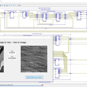
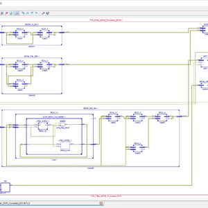
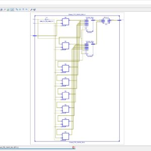
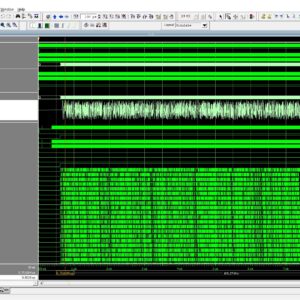
IEEE Transactions on VLSI, VLSI IEEE Project, VLSI Low Power Project, VLSI High Speed Project, VLSI Area Efficient Project, Low Cost VLSI Projects, High Speed VLSI Design projects ( CDMA, RTOS, DSP, RF, IF, etc), Low Power VLSI Design projects, Area Efficient VLSI Design projects , Audio processing VLSI Design projects, Signal Processing VLSI Design projects, Image Processing VLSI Design projects, Backend VLSI Design projects ( CMOS, TFET, BisFET, FeFET, etc), Timing & Delay Reduction VLSI Projects, Internet of Things VLSI Projects, Testing, Reliability and Fault Tolerance VLSI Projects, VLSI Applications ( Communicational, Video, Security, Sensor Networks, etc), SOC VLSI Projects, Network on Chip VLSI Projects, Wireless Communication VLSI Projects, VLSI Verifications Projects ( UVM, OVM, VVM, System Verilog).

Provide Wordlwide Online Support

We can provide Online Support Wordlwide, with proper execution, explanation and additionally provide explanation video file for execution and explanations.

24/7 Support Center

NXFEE, will Provide on 24x7 Online Support, You can call or text at +91 9789443203, or email us nxfee.innovation@gmail.com

Terms & Conditions:

Customer are advice to watch the project video file output, and before the payment to test the requirement, correction will be applicable.

After payment, if any correction in the Project is accepted, but requirement changes is applicable with updated charges based upon the requirement.

After payment the student having doubts, correction, software error, hardware errors, coding doubts are accepted.

Online support will not be given more than 3 times.

On first time explanation we can provide completely with video file support, other 2 we can provide doubt clarifications only.

If any Issue on Software license / System Error we can support and rectify that within end of day.

Extra Charges For duplicate bill copy. Bill must be paid in full, No part payment will be accepted.

After payment, to must send the payment receipt to our email id.

Powered by NXFEE INNOVATION, Pondicherry.

Call us today at : +91 9789443203 or Email us at nxfee.innovation@gmail.com

Contact us

NXFEE Development & Services

NXFEE Software Projects

Product Categories

  • 2014 (11)
  • 2015 (39)
  • 2016 (30)
  • 2017 (16)
  • 2018 (17)
  • 2019 (42)
  • 2020 (29)
  • 2021 (16)
  • 2022 (23)
  • Accessories (2)
  • Area Efficient (105)
  • High speed VLSI Design (53)
  • IEEE (15)
  • Image Processing (37)
  • Low power VLSI Design (74)
  • NOC VLSI Design (2)
  • VLSI (206)
  • VLSI 2023 (21)
  • VLSI 2024 (13)
  • VLSI 2025 (1)
  • VLSI Application / Interface and Mini Projects (21)
  • VLSI_2023 (15)

Filter by price

Price: —

Product Status

  • In stock
  • Out of stock
  • On sale

Sort by producents

    Refer and Earn

    THANK YOU

    Thank for Visit NXFEE Innovation, Get in touch with Best Semiconductor IP Development. 

    Our services

    • Company Information
    • Terms and Conditions for Sales
    • Privacy policy
    • Returns and refunds

    Quick Links

    • VLSI PHD Research
    • About NXFEE
    • Contact NXFEE

    Contact us :

    • 45, First Floor, Vivekanandar Street, Dhevan Kandappa Mudaliar Nagar, Nainarmandapam, Pondicherry - 605004. India.
    • nxfee.innovation@gmail.com
    • +91 9789443203, 0413-2968203.
    Facebook Twitter Whatsapp Email Youtube

    Copyright © 2024 Nxfee Innovation.

    Home
    Shop
    0 Cart
    More
    More
    • VLSI PHD Research
    • *** Buy VLSI Research Projects ***
    • Freelance
    • Contact
    • VLSI Mini Projects
    • Archives
    • NXFEE Youtube Channel

    WhatsApp