218 Products found
A Deblocking Filter Hardware Architecture for the High Efficiency Video Coding Standard
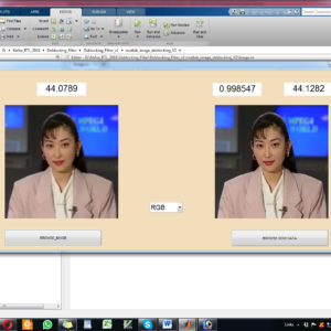
The new deblocking filter (DF) tool of the next generation High Efficiency Video Coding (HEVC) standard is one of the most time consuming algorithms in video decoding. In order to achieve real-time performance at low-power consumption, we developed a hardware accelerator for this filter. This paper proposes high throughput hardware architecture for HEVC deblocking filter employing hardware reuse to accelerate filtering decision units with a low area cost. Our architecture achieves either higher or equivalent throughput with 5X-6X lower area compared to state of-the-art deblocking filter architectures. The proposed architecture of this paper analysis the logic size, area and power consumption using Xilinx 14.2.
List of the following materials will be included with the Downloaded Backup: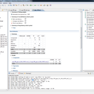
Source Code Error Detection in High Level Synthesis Functional Verification
A dynamic functional verification method that compares untimed simulations versus timed simulations for synthesizable [high-level synthesis (HLS)] behavioral descriptions (ANSI-C) is presented in this paper. This paper proposes a method that automatically inserts a set of probes into the untimed behavioral description. These probes record the status of internal signals of the behavioral description during an initial untimed simulation. These simulation results are subsequently used as golden outputs for the verification of the internal signals during a timed simulation once the behavioral description has been synthesized using HLS. Our proposed method reports any simulation mismatches and accurately pinpoints any discrepancies between the functional Software (SW) simulation and the timed simulation at the original behavioral description (source code). Our method does not only determine where to place the probes, but is also able to insert different type of probes based on the specified HLS synthesis options in order not to interfere with the HLS process, minimizing the total number of probes and the size of the data to be stored in the trace file in order to minimize the running time. Results show that our proposed method is very effective and extremely simple to use as it is fully automated using Xilinx 14.2.
List of the following materials will be included with the Downloaded Backup:
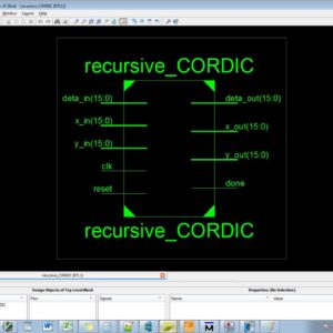
Concept Design and Implementation of Reconfigurable CORDIC
This brief presents the key concept, design strategy, and implementation of reconfigurable coordinate rotation digital computer (CORDIC) architectures that can be configured to operate either for circular or for hyperbolic trajectories in rotation as well as vectoring-modes. It can, therefore, be used to perform all the functions of both circular and hyperbolic CORDIC. We propose three reconfigurable CORDIC designs: 1) a reconfigurable rotation-mode CORDIC that operates either for circular or for hyperbolic trajectory; 2) a reconfigurable vectoring-mode CORDIC for circular and hyperbolic trajectories; and 3) a generalized reconfigurable CORDIC that can operate in any of the modes for both circular and hyperbolic trajectories. The reconfigurable CORDIC can perform the computation of various trigonometric and exponential functions, logarithms, square-root, and so on of circular and hyperbolic CORDIC using either rotation-mode or vectoring-mode CORDIC in one single circuit. It can be used in digital synchronizers, graphics processors, scientific calculators, and so on. It offers substantial saving of area complexity over the conventional design for reconfigurable applications. The proposed architecture of this paper analysis the logic size, area and power consumption using Xilinx 14.2.
List of the following materials will be included with the Downloaded Backup:
A High Speed FPGA Implementation of an RSD Based ECC Processor
In this paper, an exportable application-specific instruction-set elliptic curve cryptography processor based on redundant signed digit representation is proposed. The processor employs extensive pipelining techniques for Karatsuba–Ofman method to achieve high throughput multiplication. Furthermore, an efficient modular adder without comparison and a highthrough put modular divider, which results in a short datapath for maximized frequency, are implemented. The processor supports the recommended NIST curve P256 and is based on an extended NIST reduction scheme. The proposed architecture of this paper analysis the logic size, area and power consumption using Xilinx 14.2.
List of the following materials will be included with the Downloaded Backup:
A Multiuser Detection Algorithm in the Uplink SCFDMA System for Green Communication network
In mobile network the multiuser detection mostly in 5G networks with using communication of CDMA, SC-FDMA, UTMS, EDGE, FDMA, WI-MAX etc,. Here SC-FDMA (Single Carrier FDMA) plays major role in 5G networks even the performance of improving Low Power Consumption in Low Peak to average ratio of RF Signal Transmission. The iteration of signal transmission in the same manner of Multi User SC-FDMA requires traditional parallel and serial interference cancellation algorithm for achieving the result in large, where the algorithm is consumed to be low power consumption. In the same manner to eliminate the Multiple access RF communication, here the proposed algorithm is introduces in named Optical Weighted Parallel Interference Cancellation (OWPIC). As a result to implement the SC-FDMA with high precision then traditional Parallel Interference Cancellation(PIC) with Multi User SC-FDMA using OWPIC, and also implement this architecture in FPGA (S5LX9) and finally analysis the logic size, low power consumption, high frequency interference, radio signal interference.
List of the following materials will be included with the Downloaded Backup:
A Computation and Energy Reduction Technique for HEVC Discrete Cosine Transform
In this paper, a novel computation and energy reduction technique for High Efficiency Video Coding (HEVC) Discrete Cosine Transform (DCT) for all Transform Unit (TU) sizes is proposed. The proposed technique reduces the computational complexity of HEVC DCT significantly at the expense of slight decrease in PSNR and slight increase in bit rate by only calculating several pre-determined low frequency coefficients of TUs and assuming that the remaining coefficients are zero. It reduced the execution time of HEVC HM software encoder up to 12.74%, and it reduced the execution time of DCT operations in HEVC HM software encoder up to 37.27%. In this paper, a low energy HEVC 2D DCT hardware for all TU sizes is also designed and implemented using Verilog HDL. The proposed hardware, in the worst case, can process 53 Ultra HD (7680x4320) video frames per second. The proposed technique reduced the energy consumption of this hardware up to 18.9%. Therefore, it can be used in portable consumer electronics products that require a real-time HEVC encoder. The proposed architecture of this paper analysis the logic size, area and power consumption using Xilinx 14.2.
List of the following materials will be included with the Downloaded Backup:
Block Interleaver Design for High Data Rate Wireless Networks
With increasing data rates in wireless communication, quality of service (QoS) has become a major issue. This is more with fading channels transmitting huge volumes of data. QoS is degraded by inter-symbol interference (ISI) and related errors. One of the simplest and convenient techniques to overcome such errors is interleaving, which is used efficiently in wireless applications. It has found applications for combating burst errors that creeps up in the channel during transmission. In this paper, an efficient model of a block interleaver using a hardware description language (Verilog) is proposed. The proposed technique reduces consumption of FPGA resources to a large extent, which implies low power consumption. The proposed architecture of this paper analysis the logic size, area and power consumption using Xilinx 14.2.
List of the following materials will be included with the Downloaded Backup:
A Fully Digital Front End Architecture for ECG Acquisition System with 0.5 V Supply
This paper presents a new power-efficient electrocardiogram acquisition system that uses a fully digital architecture to reduce the power consumption and chip area. The proposed architecture is compatible with digital CMOS technology and is capable of operating with a low supply voltage of 0.5 V. In this architecture, no analog block, e.g., low-noise amplifier (LNA), and filters, and no passive elements, such as ac coupling capacitors, are used. A moving average voltage-to time converter is used, which behaves instead of the LNA and anti-aliasing filter. A digital feedback loop is employed to cancel the impact of the dc offset on the circuit, which eliminates the need for coupling capacitors. The proposed architecture of this paper area and power consumption is analysis using tanner tool.
List of the following materials will be included with the Downloaded Backup:
JF-Cut: A Parallel Graph Cut Approach for Large-Scale Image and Video
Graph cut has proven to be an effective scheme to solve a wide variety of segmentation problems in vision and graphics community. The main limitation of conventional graph-cut implementations is that they can hardly handle large images or videos because of high computational complexity. Even though there are some parallelization solutions, they commonly suffer from the problems of low parallelism (on CPU) or low convergence speed (on GPU). In this paper, we present a novel graph-cut algorithm that leverages a parallelized jump flooding technique and an heuristic push-relabel scheme to enhance the graph-cut process, namely, back-and-forth relabel, convergence detection, and block-wise push-relabel. The entire process is parallelizable on GPU, and outperforms the existing GPU-based implementations in terms of global convergence, information propagation, and performance. We design an intuitive user interface for specifying interested regions in cases of occlusions when handling video sequences. Experiments on a variety of data sets, including images (up to 15 K×10 K), videos (up to 2.5K×1.5K×50), and volumetric data, achieve highquality results and a maximum 40-fold (139-fold) speedup over conventional GPU (CPU-)-based approaches.
List of the following materials will be included with the Downloaded Backup:
Design and Analysis of Approximate Compressors for Multiplication
Inexact computing is particularly interesting for computer arithmetic designs. Implementation of 8X8 truncated multipliers using Very High Speed Integrated Circuit Hardware Description Language (VHDL). Truncated multipliers can be used in the image multiplication application. This multiplier is automatically truncating the output and reduces the power consumption and are comparing to other multipliers. The proposed architecture of this paper analysis the logic size, area and power consumption using Xilinx 14.2.
List of the following materials will be included with the Downloaded Backup:
A Robust Energy/Area-Efficient Forwarded-Clock Receiver with All-Digital Clock and Data Recovery in 28-nm CMOS for High-Density Interconnects
This paper presents a robust energy/area-efficient receiver fabricated in a 28-nm CMOS process. The receiver consists of eight data lanes plus one forwarded-clock lane supporting the hyper transport standard for high-density chip-to-chip links. The proposed all-digital clock and data recovery (ADCDR) circuit, which is well suited for today’s CMOS process scaling, enables the receiver to achieve low power and area consumption. The ADCDR can enter into open loop after lock-in to save power and avoid clock dithering phenomenon. Moreover, to compensate the open loop, a phase tracking procedure is proposed to enable the ADCDR to track the phase drift due to the voltage and temperature variations. Furthermore, the all-digital delay-locked loop circuit integrated in the ADCDR can generate accurate multiphase clocks with the proposed calibrated locking algorithm in the presence of process variations. The precise multiphase clocks are essential for the half-rate sampling and Alexander-type phase detecting. Measurement results show that the receiver can operate at a data rate of 6.4 Gbits/s with a bit error rate. The proposed architecture of this paper area and power consumption analysis using tanner tool.
List of the following materials will be included with the Downloaded Backup:
40-Gb/s 0.7-V 2:1 MUX and 1:2 DEMUX with Transformer-Coupled Technique for SerDes Interface
This paper explores the use of transformer-coupled (TC) technique for the 2:1 MUX and the 1:2 DEMUX to serialize-and-deserialize (SerDes) high-speed data sequence. The widely used current-mode logic (CML) designs of latch and multiplexer/demultiplexer (MUX/DEMUX) are replaced by the proposed TC approach to allow the more headroom and to lower the power consumption. Through the stacked transformer, the input clock pulls down the differential source voltage of the TC latch and the TC multiplexer core while alternating between the two-phase operations. With the enhanced drain-source voltage, the TC design attracts more drain current with less width-to-length ratio of NMOS than that of the CML counterpart. The source-offset voltage is decreased so that the supply voltage can be reduced. The lower supply voltage improves the power consumption and facilitates the integration with low voltage supply SerDes interface. The MUX and the DEMUX chips are fabricated in 65-nm standard CMOS process and operate at 0.7-V supply voltage. The chips are measured up to 40-Gb/s with sub-hundred milliwatts power consumption.
List of the following materials will be included with the Downloaded Backup:
Frequency-Boost Jitter Reduction for Voltage-Controlled Ring Oscillators
Ring oscillators (ROs) are popular due to their small area, modest power, wide tuning range, and ease of scaling with process technology. However, their use in many applications is limited due to poor phase noise and jitter performance. Thermal noise and flicker noise contribute jitter that decreases inversely with oscillation frequency. This paper describes a frequency boost technique to reduce jitter in ROs. We boost the internal oscillation frequency and introduce a frequency divider following the oscillator to maintain the desired output frequency. This approach offers reduced jitter as well as the opportunity to trade off output jitter with power for dynamic performance management. The oscillator has 32 operating modes, corresponding to different values for the ring size and frequency division. In a 0.5-µm CMOS process, the highest oscillation frequency achieved is 25 MHz with a root-mean-square period jitter of 54 ps and a power consumption of 817 µW at 5 V supply. A jitter model for current-starved oscillators was derived and verified by measurement; a direct relationship between oscillation frequency and jitter was derived and measured. Compared with other oscillators, this design achieves the highest performance in terms of jitter per unit interval and figure-of-merit. The performance is expected to improve in more advanced technologies. The results are summarized to offer design guidance based on the frequency boost technique. The proposed architecture of this paper area and power consumption analysis using tanner tool.
List of the following materials will be included with the Downloaded Backup:
A 0.1–3.5-GHz Duty-Cycle Measurement and Correction Technique in 130-nm CMOS
A duty-cycle correction technique using a novel pulse width modification cell is demonstrated across a frequency range of 100 MHz–3.5 GHz. The technique works at frequencies where most digital techniques implemented in the same technology node fail. An alternative method of making time domain measurements such as duty cycle and rise/fall times from the frequency domain data is introduced. The data are obtained from the equipment that has significantly lower bandwidth than required for measurements in the time domain. An algorithm for the same has been developed and experimentally verified. The correction circuit is implemented in a 0.13-µm CMOS technology and occupies an area of 0.011 mm2. It corrects to a residual error of less than 1%. The extent of correction is limited by the technology at higher frequencies. The proposed architecture of this paper area and power consumption analysis using tanner tool.
List of the following materials will be included with the Downloaded Backup:
OTA-Based Logarithmic Circuit for Arbitrary Input Signal and Its Application
In this paper, a new design procedure has been proposed for realization of logarithmic function via three phases: 1) differentiation; 2) division; and 3) integration for any arbitrary analog signal. All the basic building blocks, i.e., differentiator, divider, and integrator, are realized by operational transconductance amplifier, a current mode device. Realization of exponential, power law and hyperbolic function as the design examples claims that the proposed synthesis procedure has the potential to design a log-based nonlinear system in a systematic and hierarchical manner. The proposed architecture of this paper area and power consumption analysis using tanner tool.
List of the following materials will be included with the Downloaded Backup:
In-Field Test for Permanent Faults in FIFO Buffers of NoC Routers
Abstract:
This brief proposes an on-line transparent test technique for detection of latent hard faults which develop in first input first output buffers of routers during field operation of NoC. The technique involves repeating tests periodically to prevent accumulation of faults. A prototype implementation of the proposed test algorithm has been integrated into the router-channel interface and on-line test has been performed with synthetic self-similar data traffic. The performance of the NoC after addition of the test circuit has been investigated in terms of throughput while the area overhead has been studied by synthesizing the test hardware. In addition, an on-line test technique for the routing logic has been proposed which considers utilizing the header flits of the data traffic movement in transporting the test patterns.
List of the following materials will be included with the Downloaded Backup:
Reverse Converter Design via Parallel-Prefix Adders: Novel Components, Methodology, and Implementations
Abstract: The implementation of residue number system reverse converters based on well-known regular and modular parallel prefix adders is analyzed. The VLSI implementation results show a significant delay reduction and area × time2 improvements, all this at the cost of higher power consumption, which is the main reason preventing the use of parallel-prefix adders to achieve high-speed reverse converters in nowadays systems. Hence, to solve the high power consumption problem, novel specific hybrid parallel-prefix-based adder components those provide better tradeoff between delay and power consumption. The power, area and delay of the proposed system are analysis using Xilinx 14.2.
List of the following materials will be included with the Downloaded Backup:
FPGA Implementation of Partially Parallel Encoder Architecture for Long Polar Code
Polar coding is an encoding/decoding scheme that provably achieves the capacity of the class of symmetric binary memory-less channels. Due to the channel achieving property, the polar code has become one of the most favourable error-correcting codes. As the polar code achieves the property asymptotically, however, it should be long enough to have a good error-correcting performance. Although previous fully parallel encoder is intuitive and easy to implement, it is not suitable for long polar codes because of the huge hardware complexity required. In the brief, we analyse the encoding process in the viewpoint of very large-scale integration implementation and propose a new efficient encoder architecture that is adequate for long polar codes and effect in alleviating the hardware complexity. As the proposed encoder allows high-throughput encoding with small hardware complexity, it can be systematically applied to the design of any polar code and to any level of parallelism. Finally shown the power, area, delay report with comparison of existing work.
List of the following materials will be included with the Downloaded Backup:
Provide Wordlwide Online Support
We can provide Online Support Wordlwide, with proper execution, explanation and additionally provide explanation video file for execution and explanations.
24/7 Support Center
NXFEE, will Provide on 24x7 Online Support, You can call or text at +91 9789443203, or email us nxfee.innovation@gmail.com
Terms & Conditions:
Customer are advice to watch the project video file output, and before the payment to test the requirement, correction will be applicable.
After payment, if any correction in the Project is accepted, but requirement changes is applicable with updated charges based upon the requirement.
After payment the student having doubts, correction, software error, hardware errors, coding doubts are accepted.
Online support will not be given more than 3 times.
On first time explanation we can provide completely with video file support, other 2 we can provide doubt clarifications only.
If any Issue on Software license / System Error we can support and rectify that within end of day.
Extra Charges For duplicate bill copy. Bill must be paid in full, No part payment will be accepted.
After payment, to must send the payment receipt to our email id.
Powered by NXFEE INNOVATION, Pondicherry.
Call us today at : +91 9789443203 or Email us at nxfee.innovation@gmail.com
NXFEE Development & Services

Product Categories
- 2014 (12)
- 2015 (39)
- 2016 (31)
- 2017 (16)
- 2018 (17)
- 2019 (42)
- 2020 (29)
- 2021 (16)
- 2022 (22)
- 2023 (17)
- Area Efficient (92)
- High speed VLSI Design (49)
- IEEE (16)
- Image Processing (34)
- Low power VLSI Design (71)
- NOC VLSI Design (3)
- VLSI (180)
- VLSI Application / Interface and Mini Projects (13)
- VLSI_2023 (15)
Filter by price
Product Status
Sort by producents

Copyright © 2021 Nxfee Innovation.