9789443203
nxfee.innovation@gmail.com
Facebook Youtube Linkedin
  • VLSI PHD Research
  • *** Buy VLSI Research Projects ***
  • Freelance
  • Contact
  • VLSI Mini Projects
  • Archives
  • NXFEE Youtube Channel
What are you looking for?
Trending Searches: Low Power VLSI High Speed VLSI Signal Processing Image Processing
Popular categories
2014

2014

11 products
2015

2015

39 products
2016

2016

30 products
2017

2017

16 products
2018

2018

17 products
2019

2019

42 products
View all categories
My Account

Lost password?

0 0
0 Shopping Cart
Shopping cart (0)
Subtotal: ₹0.00

Checkout

REFER YOUR FRIENDS WHO WILL NEED VLSI PROJECTS
“EARN Rs.1,000/- FOR ONE VLSI PROJECT” ( Amount will given After Registration )
Menu Categories
  • VLSI PHD Research
  • *** Buy VLSI Research Projects ***
  • Freelance
  • Contact
  • VLSI Mini Projects
  • Archives
  • NXFEE Youtube Channel
  • Image Processing
  • 2022
  • 2016
  • VLSI 2023
  • High speed VLSI Design
  • VLSI_2023
  • Accessories
  • IEEE
  • VLSI Application / Interface and Mini Projects
  • VLSI
  • VLSI 2024
  • NOC VLSI Design
  • VLSI 2025
  • 2017
  • 2014
  • 2018
  • Area Efficient
  • 2019
  • 2015
  • 2020
  • Low power VLSI Design
  • 2021
Cart 0
0 0
0 Shopping Cart
Shopping cart (0)
Subtotal: ₹0.00

Checkout

REFER YOUR FRIENDS WHO WILL NEED VLSI PROJECTS
“EARN Rs.1,000/- FOR ONE VLSI PROJECT” ( Amount will given After Registration )
Home Shop

2014

Return to previous page

IEEE Transactions on VLSI 2014

Following Novelty based Research Projects not yet Published in Any Journal 

Customization Available for Journal Publications

Grid
List
Show
sale OFFER 44%
Floating Point Fused Dot-Product Unit
Quick View Add to cart
2014, Area Efficient, VLSI

A Floating-Point Fused Dot-Product Unit

₹18,000.00 Original price was: ₹18,000.00.₹10,000.00Current price is: ₹10,000.00.
Source : VHDL

Abstract:

A floating-point fused dot-product unit is presented that performs single-precision floating-point multiplication and addition operations on two pairs of data in a time that is only 150% the time required for a conventional floating-point multiplication. When placed and routed in a 45nm process, the fused dot-product unit occupied about 70% of the area needed to implement a parallel dot-product unit using conventional floating-point adders and multipliers. The speed of the fused dot-product is 27% faster than the speed of the conventional parallel approach. The numerical result of the fused unit is more accurate because one rounding operation is needed versus at least three for other approaches.

List of the following  materials will be included with the Downloaded Backup:
1. Source code ( Modelsim/ Xilinx/ Quartus/ DSCH3/ Microwind)
2. Existing and Proposed Project Comparison
3. Architecture Diagram
4. Algorithm with Flow chart
5. Report for Phase1 and Phase2
6. Proposed abstract document
7. Reference materials
8. Literature survey with Reference Document
9. Online Support ( Team viewer/ Ammy Admin)
sale OFFER 33%
Transmission_topology
Quick View Add to cart
2014, Low power VLSI Design

A Fully Static Topologically Compressed 21 Transistor Flip Flop With 75 Percentage of Power Saving

₹15,000.00 Original price was: ₹15,000.00.₹10,000.00Current price is: ₹10,000.00.
Source : TANNER - EDA Abstract:

An extremely low-power flip-flop (FF) named topologically-compressed flip-flop (TCFF) is proposed. As compared with conventional FFs, the FF reduces power dissipation by 75% at 0% data activity. This power reduction ratio is the highest among FFs that have been reported so far. The reduction is achieved by applying topological compression method, merger of logically equivalent transistors to an unconventional latch structure. The very small number of transistors, only three, connected to clock signal reduces the power drastically, and the smaller total transistor count assures the same cell area as conventional FFs. In addition, fully static full-swing operation makes the cell tolerant of supply voltage and input slew variation. An experimental chip design with 40 nm CMOS technology shows that almost all conventional FFs are replaceable with proposed FF while preserving the same system performance and layout area. The proposed design is analysis the power and delay by using tanner tools.

List of the following  materials will be included with the Downloaded Backup:

1. Source code ( Modelsim/ Xilinx/ Quartus/ DSCH3/ Microwind)
2. Existing and Proposed Project Comparison
3. Architecture Diagram
4. Algorithm with Flow chart
5. Report for Phase1 and Phase2
6. Proposed abstract document
7. Reference materials
8. Literature survey with Reference Document
9. Online Support ( Team viewer/ Ammy Admin)
sale OFFER 50%
Digital Spread Spectrum
Quick View Add to cart
2014, Low power VLSI Design

A Low Cost Low Power All Digital Spread Spectrum Clock Generator

₹20,000.00 Original price was: ₹20,000.00.₹10,000.00Current price is: ₹10,000.00.
Source : VHDL / Verilog HDL

Abstract:

In this brief, a low-cost low-power all-digital spread spectrum clock generator (ADSSCG) is presented. The proposed ADSSCG can provide an accurate programmable spreading ratio with process, voltage, and temperature variations. To maintain the frequency stability while performing triangular modulation, the fast-relocked mechanism is proposed. The proposed fast-relocked ADSSCG is implemented in a standard performance 90-nm CMOS process, and the active area is 200 µm × 200 µm. The experimental results show that the electromagnetic interference reduction is 14.61 dB with a 0.5% spreading ratio and 19.69 dB with a 2% spreading ratio at 270 MHz The power consumption is 443 µW at 270 MHz with a 1.0 V power supply.

List of the following  materials will be included with the Downloaded Backup:
1. Source code ( Modelsim/ Xilinx/ Quartus/ DSCH3/ Microwind)
2. Existing and Proposed Project Comparison
3. Architecture Diagram
4. Algorithm with Flow chart
5. Report for Phase1 and Phase2
6. Proposed abstract document
7. Reference materials
8. Literature survey with Reference Document
9. Online Support ( Team viewer/ Ammy Admin)
sale OFFER 50%
Floating_Point_Multiplier
Quick View Add to cart
2014, Area Efficient, VLSI

An Efficient Implementation of Floating Point Multiplier

₹20,000.00 Original price was: ₹20,000.00.₹10,000.00Current price is: ₹10,000.00.
Source : Verilog HDL

Abstract:

In this paper we describe an efficient implementation of an IEEE 754 single precision floating point multiplier targeted for Xilinx Virtex-5 FPGA. VHDL is used to implement a technology-independent pipelined design. The multiplier implementation handles the overflow and underflow cases. Rounding is not implemented to give more precision when using the multiplier in a Multiply and Accumulate (MAC) unit. With latency of three clock cycles the design achieves 301 MFLOPs. The multiplier was verified against Xilinx floating point multiplier core.

List of the following  materials will be included with the Downloaded Backup:
1. Source code ( Modelsim/ Xilinx/ Quartus/ DSCH3/ Microwind)
2. Existing and Proposed Project Comparison
3. Architecture Diagram
4. Algorithm with Flow chart
5. Report for Phase1 and Phase2
6. Proposed abstract document
7. Reference materials
8. Literature survey with Reference Document
9. Online Support ( Team viewer/ Ammy Admin)
sale OFFER 50%
Reconfigurable Pulse Shaping FIR
Quick View Add to cart
2014, High speed VLSI Design

An Efficient VLSI Architecture of a Reconfigurable Pulse Shaping FIR Interpolation

₹20,000.00 Original price was: ₹20,000.00.₹10,000.00Current price is: ₹10,000.00.
Source : VHDL Abstract:

This brief proposes a two-step optimization technique for designing a reconfigurable VLSI architecture of an interpolation filter for multi-standard digital up converter (DUC) to reduce the power and area consumption. The proposed technique initially reduces the number of multiplications per input sample and additions per input sample by 83% in comparison with individual implementation of each standard’s filter while designing a root-raised-cosine finite-impulse response filter for multi-standard DUC for three different standards. In the next step, a 2-bit binary common sub-expression (BCS)-based BCS elimination algorithm has been proposed to design an efficient constant multiplier, which is the basic element of any filter. This technique has succeeded in reducing the area and power usage by 41% and 38%, respectively, along with 36% improvement in operating frequency over a 3-bit BCS-based technique reported earlier, and can be considered more appropriate for designing the multi-standard DUC. The proposed architecture of this paper analysis the logic size, area and power consumption using Xilinx 14.2.

List of the following  materials will be included with the Downloaded Backup:

1. Source code ( Modelsim/ Xilinx/ Quartus/ DSCH3/ Microwind)
2. Existing and Proposed Project Comparison
3. Architecture Diagram
4. Algorithm with Flow chart
5. Report for Phase1 and Phase2
6. Proposed abstract document
7. Reference materials
8. Literature survey with Reference Document
9. Online Support ( Team viewer/ Ammy Admin)
sale OFFER 33%
An LUT Based RNS FIR Filter Implementation for Reconfigurable Applications
Quick View Add to cart
2014, Area Efficient, VLSI

An LUT Based RNS FIR Filter Implementation for Reconfigurable Applications

₹15,000.00 Original price was: ₹15,000.00.₹10,000.00Current price is: ₹10,000.00.
Source : Verilog HDL

Abstract:

In this work, two approaches to realize a look up table (LUT) based finite impulse response (FIR) filter using Residue Number System (RNS) are proposed. The proposed implementations take advantage of shift and add approach offered by the chosen module set. The two proposed filter architecture are compared with an earlier proposed version of reconfigurable RNS FIR filter. The filters are synthesized using Cadence RTL compiler in UMC 90 nm technology. The performance of the filters are compared in terms of Area (A), Power (P), and Delay (T). The results show that one of the proposed architecture offers significant improvement in terms of delay, while the second approach is well suited for applications that require minimal power and area. Both implementations offer advantage in area delay and power-delay-product. Proposed approaches are also verified functionally using Altera DSP Builder.

List of the following  materials will be included with the Downloaded Backup:
1. Source code ( Modelsim/ Xilinx/ Quartus/ DSCH3/ Microwind)
2. Existing and Proposed Project Comparison
3. Architecture Diagram
4. Algorithm with Flow chart
5. Report for Phase1 and Phase2
6. Proposed abstract document
7. Reference materials
8. Literature survey with Reference Document
9. Online Support ( Team viewer/ Ammy Admin)
sale OFFER 33%
Carry Select Adder
Quick View Add to cart
2014, Area Efficient

Area Delay Power Efficient Carry Select Adder

₹12,000.00 Original price was: ₹12,000.00.₹8,000.00Current price is: ₹8,000.00.

Source : VHDL

Abstract:

We are briefly discussing the logic operations are involved in the CSLA (conventional carry select adder) and the square root conventional carry select adder. We have discard the all the extra logic operations present in the conventional CSLA. In the proposed system carry selection is take place in before the final sum calculation. The proposed system achieves the optimization in the logic units. Finally the FPGA synthesis results shows to achieves a design the low power architecture for CSLA.

List of the following  materials will be included with the Downloaded Backup:

1. Source code ( Modelsim/ Xilinx/ Quartus/ DSCH3/ Microwind)
2. Existing and Proposed Project Comparison
3. Architecture Diagram
4. Algorithm with Flow chart
5. Report for Phase1 and Phase2
6. Proposed abstract document
7. Reference materials
8. Literature survey with Reference Document
9. Online Support ( Team viewer/ Ammy Admin)
sale OFFER 60%
OFDM Baseband Transceiver
Quick View Add to cart
2014, High speed VLSI Design

Design and Development of OFDM Baseband Transceiver using VIRTEX 6 FPGA Family

₹25,000.00 Original price was: ₹25,000.00.₹10,000.00Current price is: ₹10,000.00.
Source : VHDL Abstract:

Broadband Wireless Access (BWA) is a successful technology which offers high speed voice, internet connection and video.  One of the leading candidates for Broadband Wireless Access is Wi-MAX; it is a technology that compiles with the IEEE 802.16 family of standards. This paper mainly focused towards the hardware Implementation of Wireless MAN-OFDM Physical Layer of IEEE Std 802.16d Baseband Transceiver on FPGA. The RTL coding of VHDL was used, which  provides  a  high  level  design-flow  for  developing  and validating  the  communication  system  protocols  and  it provides flexibility of changes in future in order to meet real world  performance  evaluation.  This proposed system is analysis area and power. Also the outputs are verified using Xilinx 14.2.

List of the following  materials will be included with the Downloaded Backup:

1. Source code ( Modelsim/ Xilinx/ Quartus/ DSCH3/ Microwind)
2. Existing and Proposed Project Comparison
3. Architecture Diagram
4. Algorithm with Flow chart
5. Report for Phase1 and Phase2
6. Proposed abstract document
7. Reference materials
8. Literature survey with Reference Document
9. Online Support ( Team viewer/ Ammy Admin)
sale OFFER 33%
Wallace Tree Multiplier
Quick View Add to cart
2014, Area Efficient

Modified Wallace Tree Multiplier using Efficient Square Root Carry Select Adder

₹12,000.00 Original price was: ₹12,000.00.₹8,000.00Current price is: ₹8,000.00.
Source Code : VHDL  Abstract:

A multiplier is one of the key hardware blocks in most digital and high performance systems such as FIR filters,  micro processors and digital signal processors etc. A system’s  performance is generally determined by the performance of the multiplier because the multiplier is generally the slowest  element in the whole system and also it is occupying more area consuming. The Carry Select Adder (CSLA) provides a good compromise between cost and performance in carry propagation adder design. A Square Root Carry Select Adder using RCA is introduced but it offers some speed penalty. However, conventional CSLA is still area-consuming due to the dual ripple carry adder structure. In the proposed work, generally in Wallace multiplier the partial products are reduced as soon as possible and the final carry propagation path carry select adder is used. In this paper, modification is done at gate level to reduce area and power consumption. The Modified Square Root Carry Select-Adder (MCSLA) is designed using Common Boolean Logic and then compared with regular CSLA respective architectures, and this MCSLA is implemented in Wallace Tree Multiplier. This work gives the reduced area compared to normal Wallace tree multiplier. Finally an area efficient Wallace tree multiplier is designed using common Boolean logic based square root carry select adder.

List of the following  materials will be included with the Downloaded Backup:

1. Source code ( Modelsim/ Xilinx/ Quartus/ DSCH3/ Microwind)
2. Existing and Proposed Project Comparison
3. Architecture Diagram
4. Algorithm with Flow chart
5. Report for Phase1 and Phase2
6. Proposed abstract document
7. Reference materials
8. Literature survey with Reference Document
9. Online Support ( Team viewer/ Ammy Admin)
sale OFFER 33%
Parallel Self Timed Adder
Quick View Add to cart
2014, Low power VLSI Design

Recursive Approach to the Design of a Parallel Self Timed Adder

₹12,000.00 Original price was: ₹12,000.00.₹8,000.00Current price is: ₹8,000.00.
Source : TANNER

Abstract: We are briefly discussed about the 64bit parallel self timed adder based on the recursive formulation. The adder is also based on the asynchronous logic circuit and the transistor is connected in parallel. This adder is chance the path automatically, so the delay is configures automatically. The completion detection unit is given the additional support for practical implementation. The simulation is take place with 130nm CMOS technology for the adder circuit. Finally the power consumption for 64bit adder is 0.29mW.

List of the following  materials will be included with the Downloaded Backup:
1. Source code ( Modelsim/ Xilinx/ Quartus/ DSCH3/ Microwind)
2. Existing and Proposed Project Comparison
3. Architecture Diagram
4. Algorithm with Flow chart
5. Report for Phase1 and Phase2
6. Proposed abstract document
7. Reference materials
8. Literature survey with Reference Document
9. Online Support ( Team viewer/ Ammy Admin)
sale OFFER 33%
Sharing Logic for Built In Generation of Functional Broadside Tests
Quick View Add to cart
2014, Area Efficient

Sharing Logic for Built In Generation of Functional Broadside Tests

₹12,000.00 Original price was: ₹12,000.00.₹8,000.00Current price is: ₹8,000.00.
Source : VHDL

Abstract: We are discussed about the built in generation for logic blocks. The advantage of this technique is identifying the similar characteristics of the each logical block. Functional broadside tests are important for addressing overtesting of delay faults as well as avoiding excessive power dissipation during test application. Finally to analysis the performance of the built in generation technique and compare to existing system.

List of the following  materials will be included with the Downloaded Backup:
1. Source code ( Modelsim/ Xilinx/ Quartus/ DSCH3/ Microwind)
2. Existing and Proposed Project Comparison
3. Architecture Diagram
4. Algorithm with Flow chart
5. Report for Phase1 and Phase2
6. Proposed abstract document
7. Reference materials
8. Literature survey with Reference Document
9. Online Support ( Team viewer/ Ammy Admin)
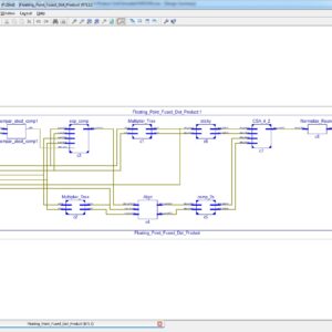
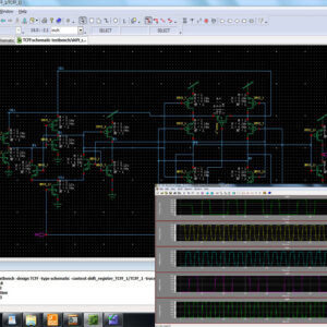
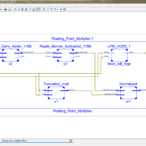
IEEE Transactions on VLSI, VLSI IEEE Project, VLSI Low Power Project, VLSI High Speed Project, VLSI Area Efficient Project, Low Cost VLSI Projects, High Speed VLSI Design projects ( CDMA, RTOS, DSP, RF, IF, etc), Low Power VLSI Design projects, Area Efficient VLSI Design projects , Audio processing VLSI Design projects, Signal Processing VLSI Design projects, Image Processing VLSI Design projects, Backend VLSI Design projects ( CMOS, TFET, BisFET, FeFET, etc), Timing & Delay Reduction VLSI Projects, Internet of Things VLSI Projects, Testing, Reliability and Fault Tolerance VLSI Projects, VLSI Applications ( Communicational, Video, Security, Sensor Networks, etc), SOC VLSI Projects, Network on Chip VLSI Projects, Wireless Communication VLSI Projects, VLSI Verifications Projects ( UVM, OVM, VVM, System Verilog.

Provide Wordlwide Online Support

We can provide Online Support Wordlwide, with proper execution, explanation and additionally provide explanation video file for execution and explanations.

24/7 Support Center

NXFEE, will Provide on 24x7 Online Support, You can call or text at +91 9789443203, or email us nxfee.innovation@gmail.com

Terms & Conditions:

Customer are advice to watch the project video file output, and before the payment to test the requirement, correction will be applicable.

After payment, if any correction in the Project is accepted, but requirement changes is applicable with updated charges based upon the requirement.

After payment the student having doubts, correction, software error, hardware errors, coding doubts are accepted.

Online support will not be given more than 3 times.

On first time explanation we can provide completely with video file support, other 2 we can provide doubt clarifications only.

If any Issue on Software license / System Error we can support and rectify that within end of day.

Extra Charges For duplicate bill copy. Bill must be paid in full, No part payment will be accepted.

After payment, to must send the payment receipt to our email id.

Powered by NXFEE INNOVATION, Pondicherry.

Call us today at : +91 9789443203 or Email us at nxfee.innovation@gmail.com

Contact us

NXFEE Development & Services

NXFEE Software Projects

Product Categories

  • 2014 (11)
  • 2015 (39)
  • 2016 (30)
  • 2017 (16)
  • 2018 (17)
  • 2019 (42)
  • 2020 (29)
  • 2021 (17)
  • 2022 (23)
  • Accessories (4)
  • Area Efficient (107)
  • High speed VLSI Design (53)
  • IEEE (15)
  • Image Processing (38)
  • Low power VLSI Design (74)
  • NOC VLSI Design (2)
  • VLSI (209)
  • VLSI 2023 (21)
  • VLSI 2024 (14)
  • VLSI 2025 (1)
  • VLSI Application / Interface and Mini Projects (24)
  • VLSI_2023 (15)

Filter by price

Price: —

Product Status

  • In stock
  • Out of stock
  • On sale

Sort by producents

    Refer and Earn

    THANK YOU

    Thank for Visit NXFEE Innovation, Get in touch with Best Semiconductor IP Development. 

    Our services

    • Company Information
    • Terms and Conditions for Sales
    • Privacy policy
    • Returns and refunds

    Quick Links

    • VLSI PHD Research
    • About NXFEE
    • Contact NXFEE

    Contact us :

    • 45, First Floor, Vivekanandar Street, Dhevan Kandappa Mudaliar Nagar, Nainarmandapam, Pondicherry - 605004. India.
    • nxfee.innovation@gmail.com
    • +91 9789443203, 0413-2968203.
    Facebook Twitter Whatsapp Email Youtube

    Copyright © 2024 Nxfee Innovation.

    Home
    Shop
    0 Cart
    More
    More
    • VLSI PHD Research
    • *** Buy VLSI Research Projects ***
    • Freelance
    • Contact
    • VLSI Mini Projects
    • Archives
    • NXFEE Youtube Channel

    WhatsApp