IEEE Transactions on VLSI 2021
Following Novelty based Research Projects not yet Published in Any Journal
Customization Available for Journal Publications
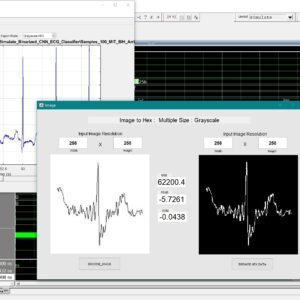
Resource and Energy Efficient Implementation of ECG Classifier using Binarized CNN for Edge AI Devices
Base Paper Abstract:
Wearable Artificial Intelligence-of-Things (AIoT) devices demand smart gadgets that are both resource and energy-efficient. In this paper, we explore efficient implementation of binary convolutional neural network employing function merging and block reuse techniques. The hardware implemented in field programmable gate array (FPGA) platform can classify ventricular beat in electrocardiogram achieving accuracy of 97.5%, sensitivity of 85.7%, specificity of 99.0%, precision of 92.3%, and F1-score of 88.9% while consuming only 10.5-µW of dynamic power dissipation.
List of the following materials will be included with the Downloaded Backup: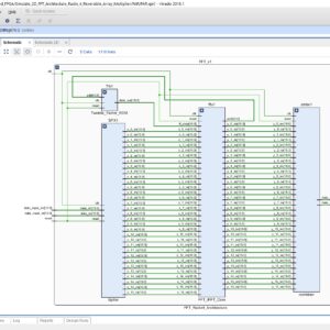
Design of SEU Tolerant 2D-FFT in SRAM-based FPGA
Base Paper Abstract:
2-Dimensional fast Fourier transform (FFT) has been widely used in radar signal process. Due to the need for high performance, field programmable gate array (FPGA) is an ideal hardware device for this application. For space-borne radar platform such as synthetic aperture radar (SAR), single-event upsets (SEUs) can cause lots of soft errors in static random access memory (SRAM) based FPGA. As to this, protecting the 2D-FFT implemented in FPGA from SEUs is very important. In this article, we analyze the critical weakness induced by SEUs in the 2D-FFT process, and then a 2D-FFT design with high SEU resilience is presented. The design utilizes the advantage of several anti-SEU methods. For butterfly control in FFT, partially triple modular redundancy (TMR) is used. For data buffers, error correction code (ECC) is applied to read and write operation. Furthermore, safe finite state machine (FSM) is adopted by important control registers. Fault injection results show that all these reinforcement technologies contribute to enhance the ability to mitigate the SEU effects.
List of the following materials will be included with the Downloaded Backup: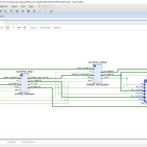
FPGA Implementation of D8PSK Demodulator
Base Paper Abstract:
Differential phase shift keying (DPSK) is a modulation scheme that facilitates non coherent demodulation and is employed for various applications such as Wireless Local Area Networks (WLANs), Bluetooth and RFID communication. In this paper, design, development and hardware implementation of a new demapping scheme for Differential 8-PSK (D8PSK) demodulator on a Zynq 7000 FPGA based ZED board is proposed using the concepts of model based design. The proposed work can be easily extended to other M-ary DPSK schemes.
List of the following materials will be included with the Downloaded Backup:
A Pipelined Reduced Complexity Two Stages Parallel LMS Structure for Adaptive Beam forming
Base Paper Abstract:
In this paper, we propose a reduced complexity parallel least mean square structure (RC-pLMS) for adaptive beamforming and its pipelined hardware implementation. RC-pLMS is formed by two least mean square (LMS) stages operating in parallel (pLMS), where the overall error signal is derived as a combination of individual stage errors. The pLMS is further simplified to remove the second independent set of weights resulting in a reduced complexity pLMS (RC-pLMS) design. In order to obtain a pipelined hardware architecture of our proposed RC-pLMS algorithm, we applied the delay and sum relaxation technique (DRC-pLMS). Convergence, stability and quantization effect analysis are performed to determine the upper bound of the step size and assess the behavior of the system. Computer simulations demonstrate the outstanding performance of the proposed RC-pLMS in providing accelerated convergence and reduced error floor while preserving a LMS identical O(N) complexity, for an antenna array of N elements. Synthesis and implementation results show that the proposed design achieves a significant increase in the maximum operating frequency over other variants with minimal resource usage. Additionally, the resulting beam radiation pattern show that the finite precision DRC-pLMS implementation presents similar behavior of the infinite precision theoretical results.
List of the following materials will be included with the Downloaded Backup: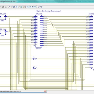
FPGA Implementation of the Adaptive Digital Beamforming for Massive Array
Base Paper Abstract:
With the rise of 5G networks and the increasing number of communication devices, improving communication quality is essential. One approach is adaptive digital beamforming, which adjusts an antenna array’s radiation pattern based on the desired received signal. Adaptation based on Least-Mean Squared (LMS) and its variants is still one of the most common literature methods. Although LMS techniques present good computational performance, the increase in antennas’ numbers led to high-performance hardware. Platforms such as Field Programmable Gate Arrays (FPGAs), designed for massive array systems, enables high-performance energy-efficient architectures. This work proposes a parallel implementation of a massive array beamforming composed of a spatial filter and adaptation unit based on LMS on FPGA. The proposed design presents ten times fewer hardware requirements and 30 times less power consumption than state of the art.
List of the following materials will be included with the Downloaded Backup:
Approximate Pruned and Truncated Haar Discrete Wavelet Transform VLSI Hardware for Energy-Efficient ECG Signal Processing
Abstract:
The approximate computing paradigm emerged as a key alternative for trading off accuracy and energy efficiency. Error-tolerant applications, such as multimedia and signal processing, can process the information with lower-than-standard accuracy at the circuit level while still fulfilling a good and acceptable service quality at the application level. The automatic detection of R-peaks in an electrocardiogram (ECG) signal is the essential step preceding ECG processing and analysis. The Haar discrete wavelet transform (HDWT) is a low-complexity pre-processing filter suitable to detect ECG R-peaks in embedded systems like wearable devices, which are incredibly energy constrained. This work presents an approximate HDWT hardware architecture for ECG processing at very high energy efficiency. Our best-proposal employing pruning within the approximate HDWT hardware architecture requires just seven additions. The use of a truncation technique to improve energy efficiency is also investigated herein by observing the evolution of the signal-to-noise ratio and the ultimate impact in the ECG peak-detection application. This research finds that our HDWT approximate hardware architecture proposal accepts higher truncation levels than the original HDWT. In summary: Our results show about 9 times energy reduction when combining our HDWT matrix approximation proposal with the pruning and the highest acceptable level of truncation while still maintaining the R-peak detection performance accuracy of 99.68% on average.
List of the following materials will be included with the Downloaded Backup: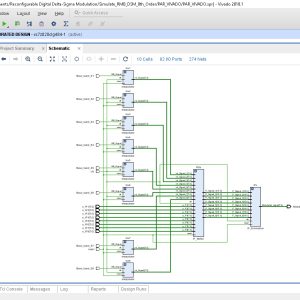
Reconfigurable Digital Delta-Sigma Modulation Transmitter Architecture for Concurrent Multi-Band Transmission
Abstract:
This paper presents a reconfigurable delta-sigma modulation (DSM) architecture for concurrent multi-band transmission. The reconfigurability in terms of carrier spacing and the number of simultaneous carrier transmission is useful for applications such as carrier aggregation in 5G. This paper uses 4th order reconfigurable multi-band DSM (RMB-DSM) such that the zeros of the noise transfer function can be reconfigured to fall at multiple frequencies, where the carriers are being aggregated. The quantization noise between the transmission bands is a critical issue in the case of multi-band transmission. Therefore, a multi-band additional noise shaping (ANS) function is also introduced, which generates notches around each carrier and reduces the noise level between the multiple pass-bands. The proposed scheme has been validated in simulation, as well as in experiment for aggregating up to four 15 MHz long term evolution (LTE) signals with an overall aggregated bandwidth of 60 MHz. Measurement results show a 10-25% improvement in coding efficiency and 15-35 dB improvement in noise level near the operating frequency band using the proposed multiband augmented noise shaping technique, as compared to the standard DSM. The corresponding improvement of 8% in the overall efficiency is observed by using the proposed multi-band augmented noise shaping technique.
List of the following materials will be included with the Downloaded Backup: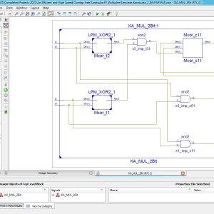
An Efficient and High Speed Overlap Free Karatsuba Based Finite Field Multiplier for FPGA Implementation
Abstract:
Cryptography systems have become inseparable parts of almost every communication device. Among cryptography algorithms, public-key cryptography, and in particular elliptic curve cryptography (ECC), has become the most dominant protocol at this time. In ECC systems, polynomial multiplication is considered to be the most slow and area consuming operation. This article proposes a novel hardware architecture for efficient field-programmable gate array (FPGA) implementation of Finite field multipliers for ECC. Proposed hardware was implemented on different FPGA devices for various operand sizes, and performance parameters were determined. Comparing to state-of-the art works, the proposed method resulted in a lower combinational delay and area–delay product indicating the efficiency of design.
List of the following materials will be included with the Downloaded Backup:
A Low Cost and High Throughtput FPGA Implementation of the Retinex Algorithm for Real Time Video Enhancement
Abstract:
For video applications in a special environment such as medical imaging, space exploration, and underwater exploration, the video captured by an image sensor is often deteriorated because of low lighting conditions. Therefore, it is necessary to enhance the part of the image that is too dark to distinguish details while maintaining the remaining part with the same brightness. The retinex algorithm is widely used to restore naturalness of a video, especially exhibiting outstanding performance in the enhancement of a dark area. However, it demands large computational complexity because of its intricate structure, such as the Gaussian filter and exponentiation operations, and consequently, it is difficult to process in real time. This article presents a low-cost and high-throughput design of the retinex video enhancement algorithm. The hardware (HW) design is implemented using a field-programmable gate array (FPGA), and it supports a throughput of 60 frames/s for a 1920 × 1080 image with negligible latency. The proposed FPGA design minimizes HW resources while maintaining the quality and the performance by using a small line buffer instead of a frame buffer, by applying the concept of approximate computing for the complex Gaussian filter, and by designing a new and nontrivial exponentiation operation. The proposed design makes it possible to significantly reduce HW resources (up to 79.22% of total resources) compared to existing systems and is compatible with commercialized devices through the standard HDMI/DVI video ports.
List of the following materials will be included with the Downloaded Backup:
High Performance Accurate and Approximate Multipliers for FPGA based Hardware Accelerators
Abstract:
Multiplication is one of the widely used arithmetic operations in a variety of applications, such as image/video processing and machine learning. FPGA vendors provide high performance multipliers in the form of DSP blocks. These multipliers are not only limited in number and have fixed locations on FPGAs but can also create additional routing delays and may prove inefficient for smaller bit-width multiplications. Therefore, FPGA vendors additionally provide optimized soft IP cores for multiplication. However, in this work, we advocate that these soft multiplier IP cores for FPGAs still need better designs to provide high-performance and resource efficiency. Towards this, we present generic area-optimized, low-latency accurate and approximate soft-core multiplier architectures, which exploit the underlying architectural features of FPGAs, i.e., look-up table (LUT) structures and fast carry chains to reduce the overall critical path delay and resource utilization of multipliers. Compared to Xilinx multiplier LogiCORE IP, our proposed unsigned and signed accurate architecture provides up to 25% and 53% reduction in LUT utilization, respectively, for different sizes of multipliers. Moreover, with our unsigned approximate multiplier architectures, a reduction of up to 51% in the critical path delay can be achieved with an insignificant loss in output accuracy when compared with the LogiCORE IP. For illustration, we have deployed the proposed multiplier architecture in accelerators used in image and video applications, and evaluated them for area and performance gains.
List of the following materials will be included with the Downloaded Backup: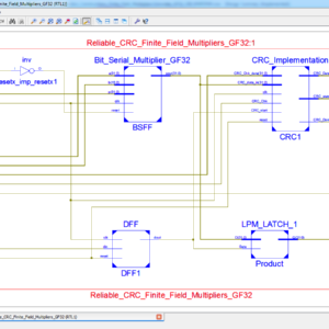
Reliable CRC Based Error Detection Constructions for Finite Field Multipliers With Applications in Cryptography
Abstract:
Finite-field multiplication has received prominent attention in the literature with applications in cryptography and error-detecting codes. For many cryptographic algorithms, this arithmetic operation is a complex, costly, and time-consuming task that may require millions of gates. In this work, we propose efficient hardware architectures based on cyclic redundancy check (CRC) as error-detection schemes for postquantum cryptography (PQC) with case studies for the Luov cryptographic algorithm. Luov was submitted for the National Institute of Standards and Technology (NIST) PQC standardization competition and was advanced to the second round. The CRC polynomials selected are in-line with the required error-detection capabilities and with the field sizes as well. We have developed verification codes through which software implementations of the proposed schemes are performed to verify the derivations of the formulations. Additionally, hardware implementations of the original multipliers with the proposed error-detection schemes are performed over a Xilinx field-programmable gate array (FPGA), verifying that the proposed schemes achieve high error coverage with acceptable overhead.
List of the following materials will be included with the Downloaded Backup: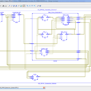
FPGA Based High Definition SPWM Generation With Harmonic Mitigation Property
Abstract:
High-resolution sinusoidal pulse width modulation (SPWM) switching is beneficial in order to achieve compact size and fine sinusoidal output of dc–ac converters. In this article, a novel field-programmable gate array (FPGA) based high-definition SPWM (HD-SPWM) architecture is proposed for adopting a scheme of integrating a lower frequency PWM train to a high-frequency SPWM train in order to suppress inverter output harmonics while achieving high resolution output. An optimized FPGA based two-stage finite-state-machine (FSM) architecture is designed, where the initial stage decides pulse widths of a lower frequency PWM train based on the premeditated pulse width of the high-frequency SPWM train, whereas in the final stage, lower frequency PWM pulse widths are integrated with the high-frequency SPWM pulse widths to generate updated pulse widths of high-frequency SPWM, i.e., HD-SPWM. Moreover, a pre-formulation mathematical model is established for the calculation of duty-cycle count values of pulse trains to support the online adjustment of modulation index (MI) of the HD-SPWM. The proposed generation has the benefits of harmonic mitigation, online fine adjustment of MI, low-processing time, and requirement of a minor segment of a medium-sized FPGA; thereby, providing a good tradeoff between larger designs and higher performance. Theoretical calculations, characteristics, and design contemplations are specified, and the HD-SPWM generation is demonstrated through experimentation with a Xilinx Spartan-3 FPGA board.
List of the following materials will be included with the Downloaded Backup: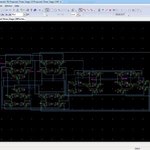
A Three Stage Comparator and Its Modified Version With Fast Speed and Low Kickback
Abstract:
This brief presents a three-stage comparator and its modified version to improve the speed and reduce the kickback noise. Compared to the traditional two-stage comparators, the three-stage comparator in this work has an extra amplification stage, which enlarges the voltage gain and increases the speed. Unlike the traditional two-stage structure that uses pMOS input pair in the regeneration stage, the three-stage comparator makes it possible to use nMOS input pairs in both the regeneration stage and the amplification stage, further increasing the speed. Furthermore, in the proposed modified version of three-stage comparator, a CMOS input pair is adopted at the amplification stage. This greatly reduces the kickback noise by canceling out the nMOS kickback through the pMOS kickback. It also adds an extra signal path in the regeneration stage, which helps increase the speed further. For easy comparison, both the conventional two-stage and the proposed three-stage comparators are implemented in the same 130-nm CMOS process. Measured results show that the modified version of three-stage comparator improves the speed by 32%, and decreases the kickback noise by ten times. This improvement is not at the cost of increased input referred offset or noise.
List of the following materials will be included with the Downloaded Backup: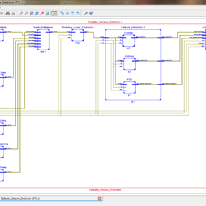
FPGA Implementation of Epileptic Seizure Detection Using ELM Classifier Detection Using ELM Classifier
Abstract:
Electroencephalography (EEG) Signals are widely used to determine the brain disorders. The Electrical activity of human brain is recorded in the form of EEG signal. The abnormal Electrical activity of the human brain is called as epileptic seizure. In epilepsy patients, the seizure occurs at unpredictable times and it causes sudden death. Detection and Prediction of Epileptic seizure is performed by analyzing the EEG signal. The EEG signal of human brain is random in nature, hence detection of seizure in EEG signal is challenging task. Hardware implementation of Epileptic seizure detection system is necessary for real time applications. In this work an accurate approach is used to identify the Epileptic seizure and that is implemented in FPGA (Field Programmable Gate Array).The hardware implementation of epileptic seizure detection algorithm is done using Xilinx System generator tool. In the first step the EEG signal is extracted from the human brain and it is filtered by using Finite Impulse response (FIR) band pass filter. The band pass filter separates the EEG signal into delta, theta, alpha, beta and gamma brain rhythms. The band separated brain signal is modeled by linear prediction theory. In the next step features are extracted from the modeled EEG signal and the classification of normal or seizure signal is done by using Extreme Learning Machine (ELM) classifier. The EEG signals used in this paper were obtained from Epilepsy Center at the University of Bonn, Germany. The hardware architecture, Look up tables, resource utilization, Accuracy and power consumption of the algorithm is analyzed using xilinx zynq7000 all programmable soc.
List of the following materials will be included with the Downloaded Backup:
ReLOPE: Resistive RAM-Based Linear First-Order Partial Differential Equation Solver
Abstract:
Data movement between memory and processing units poses an energy barrier to Von-Neumann-based architectures. In-memory computing (IMC) eliminates this barrier. RRAM-based IMC has been explored for data-intensive applications, such as artificial neural networks and matrix-vector multiplications that are considered as “soft” tasks where performance is a more important factor than accuracy. In “hard” tasks such as partial differential equations (PDEs), accuracy is a determining factor. In this brief, we propose ReLOPE, a fully RRAM crossbar-based IMC to solve PDEs using the Runge–Kutta numerical method with 97% accuracy. ReLOPE expands the operating range of solution by exploiting shifters to shift input data and output data. ReLOPE range of operation and accuracy can be expanded by using fine-grained step sizes by programming other RRAMs on the BL. Compared to software-based PDE solvers, ReLOPE gains 31.4× energy reduction at only 3% accuracy loss.
List of the following materials will be included with the Downloaded Backup: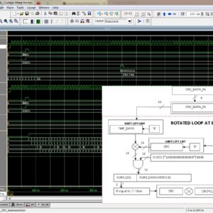
Low-Cost and Programmable CRC Implementation Based on FPGA
Abstract:
Cyclic redundancy check (CRC) is a well-known error detection code that is widely used in Ethernet, PCIe, and other transmission protocols. The existing FPGA-based implementation solutions encounter the problem of excessive resource utilization in high-performance scenarios. The padding zeros problem and the introduction of programmability further exacerbate this problem. In this brief, the stride-by-5 algorithm is proposed to achieve the optimal utilization of FPGA resources. The pipelining go back algorithm is proposed to solve the padding zeros problem. The method of reprogramming by HWICAP is proposed to realize programmability with small and constant resource utilization. The experimental results show that the resource utilization of the proposed non-segmented architecture is 80.7%-87.5% and 25.1%-46.2% lower than that of two state of-the-art FPGA-based CRC implementations, and the proposed segmented architecture has lower resource utilization, by 81.7%- 85.9% and 2.9%-20.8%, than two state-of-the-art architectures. Furthermore, throughput and programmability are guaranteed.
List of the following materials will be included with the Downloaded Backup:
Design of ultra-low power consumption approximate 4-2 compressors based on the compensation characteristic
Abstract:
Approximate computing is tentatively applied in some digital signal processing applications which have an inherent tolerance for erroneous computing results. The approximate arithmetic blocks are utilized in them to improve the electrical performance of these circuits. Multiplier is one of the fundamental units in computer arithmetic blocks. Moreover, the 4-2 compressors are widely employed in the parallel multipliers to accelerate the compression process of partial products. In this paper, three novel approximate 4-2 compressors are proposed and utilized in 8-bit multipliers. Meanwhile, an error-correcting module (ECM) is presented to promote the error performance of approximate multiplier with the proposed 4-2 compressors. In this paper, the number of the approximate 4-2 compressor’s outputs is innovatively reduced to one, which brings further improvements in the energy efficiency. Compared with the exact 4-2 compressors, the simulation results indicate that the proposed approximate compressors UCAC1, UCAC2, UCAC3 achieve 24.76%, 51.43%, and 66.67% reduction in delay, 71.76%, 83.06%, and 93.28% reduction in power and 54.02%, 79.32%, and 93.10% reduction in area, respectively. And the utilization of these proposed compressors in 8-bit multipliers brings 49.29% reduction of power consumption on average.
List of the following materials will be included with the Downloaded Backup:IEEE Transactions on VLSI, VLSI IEEE Project, VLSI Low Power Project, VLSI High Speed Project, VLSI Area Efficient Project, Low Cost VLSI Projects, High Speed VLSI Design projects ( CDMA, RTOS, DSP, RF, IF, etc), Low Power VLSI Design projects, Area Efficient VLSI Design projects , Audio processing VLSI Design projects, Signal Processing VLSI Design projects, Image Processing VLSI Design projects, Backend VLSI Design projects ( CMOS, TFET, BisFET, FeFET, etc), Timing & Delay Reduction VLSI Projects, Internet of Things VLSI Projects, Testing, Reliability and Fault Tolerance VLSI Projects, VLSI Applications ( Communicational, Video, Security, Sensor Networks, etc), SOC VLSI Projects, Network on Chip VLSI Projects, Wireless Communication VLSI Projects, VLSI Verifications Projects ( UVM, OVM, VVM, System Verilog.
Provide Wordlwide Online Support
We can provide Online Support Wordlwide, with proper execution, explanation and additionally provide explanation video file for execution and explanations.
24/7 Support Center
NXFEE, will Provide on 24x7 Online Support, You can call or text at +91 9789443203, or email us nxfee.innovation@gmail.com
Terms & Conditions:
Customer are advice to watch the project video file output, and before the payment to test the requirement, correction will be applicable.
After payment, if any correction in the Project is accepted, but requirement changes is applicable with updated charges based upon the requirement.
After payment the student having doubts, correction, software error, hardware errors, coding doubts are accepted.
Online support will not be given more than 3 times.
On first time explanation we can provide completely with video file support, other 2 we can provide doubt clarifications only.
If any Issue on Software license / System Error we can support and rectify that within end of day.
Extra Charges For duplicate bill copy. Bill must be paid in full, No part payment will be accepted.
After payment, to must send the payment receipt to our email id.
Powered by NXFEE INNOVATION, Pondicherry.
Call us today at : +91 9789443203 or Email us at nxfee.innovation@gmail.com
NXFEE Development & Services

Product Categories
- 2014 (11)
- 2015 (39)
- 2016 (30)
- 2017 (16)
- 2018 (17)
- 2019 (42)
- 2020 (29)
- 2021 (17)
- 2022 (23)
- Accessories (43)
- Area Efficient (116)
- High speed VLSI Design (56)
- IEEE (15)
- Image Processing (40)
- Low power VLSI Design (97)
- NOC VLSI Design (2)
- VLSI (249)
- VLSI 2023 (21)
- VLSI 2024 (18)
- VLSI 2025 (30)
- VLSI 2026 (3)
- VLSI Application / Interface and Mini Projects (31)
- VLSI_2023 (15)
Filter by price
Product Status
Sort by producents

Copyright © 2026 Nxfee Innovation.