IEEE Transactions on VLSI 2020
Following Novelty based Research Projects not yet Published in Any Journal
Customization Available for Journal Publications
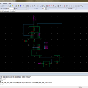
A 2.5-V 8-Bit Low power SAR ADC using POLC and SMTCMOS D-FF for IoT Applications
Abstract:
A 2.5-V 8-bit low force and efficient Successive Approximation Register Analog-to-Digital converter (SAR-ADC) utilizing a Principled Open Loop Comparator (POLC) and Switched Multi-Threshold Complementary Metal Oxide Semiconductor (SMTCMOS) D-FF shift Register. In light of high proficiency and low force applications SAR-ADC is increasingly well known, yet it experience the ill effects of resolution and speed confinements. To defeat the above issue proposed a systematic methodology uses low force POLC based SAR-ADC is structured. Considering about the resolution, speed and compact design of 8- bit SAR-ADC, the proposed POLC strategy reasonably diminishes the propagation delay by 37% and decreases the force utilization by 62% appeared differently in relation to the standard system. A D-flip flop is planned to employ SMTCMOS procedure which has low force utilization and productively decline the leakage power. All the above circuits are simulated by using TANNER-EDA tool in 0.25μm CMOS technology produces 97% Efficiency.
List of the following materials will be included with the Downloaded Backup:
A Compact 0.3 V Class AB Bulk Driven OTA
Abstract:
In this article, a new solution for an ultralow-voltage (ULV) ultralow-power (ULP) operational transconductance amplifier (OTA) is presented. Thanks to the combination of a low-voltage bulk-driven nontailed differential stage with the multipath Miller zero compensation technique, a simple class AB power-efficient ULV structure has been obtained, which can operate from supply voltages less than the threshold voltages of the employed MOS transistors, while offering rail-to-rail input common-mode range at the same time. The proposed OTA was fabricated using the 180-nm CMOS process from Taiwan Semiconductor Manufacturing Company (TSMC) and can operate from VDD ranging from 0.3 to 0.5 V. The 0.3-V version dissipates only 12.6 nW of power while showing a 64.7-dB voltage gain at 1-Hz, 2.96-kHz gain-bandwidth product, and a 4.15-V/ms average slew-rate at 30-pF load capacitance. The measured results agree well with simulations.
List of the following materials will be included with the Downloaded Backup:
A Design Implementation and Comparative Analysis of Advanced Encryption Standard (AES) Algorithm on FPGA
Abstract:
As the technology is getting advanced continuously the problem for the security of data is also increasing. The hackers are equipped with new advanced tools and techniques to break any security system. Therefore people are getting more concern about data security. The data security is achieved by either software or hardware implementations. In this work Field Programmable Gate Arrays (FPGA) device is used for hardware implementation since these devices are less complex, more flexible and provide more efficiency. This work focuses on the hardware execution of one of the security algorithms that is the Advanced Encryption Standard (AES) algorithm. The AES algorithm is executed on Vivado 2014.2 ISE Design Suite and the results are observed on 28 nanometers (nm) Artix-7 FPGA. This work discusses the design implementation of the AES algorithm and the resources consumed in implementing the AES design on Artix-7 FPGA. The resources which are consumed are as follows- Slice Register (SR), Look-Up Tables (LUTs), Input/Output (I/O) and Global Buffer (BUFG).
List of the following materials will be included with the Downloaded Backup:
A High-Performance Multiply-Accumulate Unit by Integrating Additions and Accumulations into Partial Product Reduction Process
Abstract:
In this paper, we propose a low-power high-speed pipeline multiply-accumulate (MAC) architecture. In a conventional MAC, carry propagations of additions (including additions in multiplications and additions in accumulations) often lead to large power consumption and large path delay. To resolve this problem, we integrate a part of additions into the pa rtial product reduction (PPR) process. In the proposed MAC architecture, the addition and accumulation of higher significance bits are not performed until the PPR process of the next multiplication. To correctly deal with the overflow in the PPR process, a small-size adder is designed to accumulate the total number of carries. Compared with previous works, experimental results show that the proposed MAC architecture can greatly reduce both power consumption and circuit area under the same timing constraint.
List of the following materials will be included with the Downloaded Backup:
A Highly Efficient Conditional Feed through Pulsed Flip Flop for High Speed Applications
Abstract:
A novel type of highly efficient conditional feed through pulse-triggered flip-flop (P-FF) is proposed and demonstrated. The data-to-output (D-to-Q) delay in this circuit was highly optimized using pre discharging and conditional signal feed through schemes. Power consumption was also reduced using a shared pulse generator and an output feedback-controlled conditional keeper, which diminished the floating status of the internal node. The driving strength of this design was further enhanced by including an additional pull-down path at the output node. Various post layout simulation results applied to 16-nm Fin FET technology demonstrated a higher energy efficiency (at all input data toggle rates) for the proposed topology than comparable P-FF devices. Notably, the proposed model achieved a 62% D-to-Q delay reduction, compared to a transmission gate FF, outperforming the device by more than 66% in terms of power efficiency and 87% in energy efficiency (at a 50% input data toggle rate). Improvements were even more significant in comparison with other conventional P-FFs. These results suggest the proposed design to be a viable new option for high-efficiency sequential elements in high-speed applications.
List of the following materials will be included with the Downloaded Backup:
A Review on Fundamentals of Ternary Reversible Logic Circuits
Abstract:
One of the main motivations for using ternary logic systems is the amount of information per circuit line is higher as compared to the corresponding binary logic representation, thereby leading to more compact circuit realizations. This is particularly attractive for quantum computing as quarts are expensive resources and minimizing their number is one of the main objectives during synthesis. Therefore, ternary reversible logic synthesis has drawn significant attention among researchers. It deals with fundamental unit of information called quarts that can exist in one of the three states |0, |1 and |2. Hence, the aim of this paper is to bridge the knowledge gap for the beginners in this domain than searching the entire space. Therefore, the present work discusses the basic concepts of ternary reversible logic and ternary reversible gates. The detailed discussion of the various ternary reversible logic synthesis will enable the beginners in this domain to understand the ternary reversible logic in a better way.
List of the following materials will be included with the Downloaded Backup:
A Sub-200nW All-in-One Bandgap Voltage and Current Reference without Amplifiers
Abstract:
This brief presents a low-power and high-precision bandgap voltage and current reference (BGVCR) in one simple circuit for battery-powered applications. All the amplifiers have been eliminated in the proposed circuit. The voltage reference is derived from the bandgap topology, and the current reference is obtained by summing a proportional-to-absolute-temperature (PTAT) current and a complementary-to-absolute-temperature (CTAT) current. Therefore, the temperature coefficient of the current reference can be optimized. Besides, a pseudo-cascode structure and a simple line sensitivity enhancement circuit are adopted to improve the current mirror accuracy and line sensitivity. The proposed circuit is fabricated in a 0.18-μm deep N-well CMOS process with an active area of 0.063 mm2. The measured VREF and IREF are 1.2 V and 51 nA, respectively. The VREF and IREF show measured average temperature coefficients of 32.7 ppm/℃ and 89 ppm/℃ at a temperature of -45 to 125 ℃ and standard deviations of 0.17 % and 1.15 %, respectively. In the supply voltage range of 2 to 5 V, the line sensitivities of voltage and current are 0.058%/V and 1.76%/V, respectively. The minimum supply voltage is 2 V with a total power consumption of 192 nW at room temperature.
List of the following materials will be included with the Downloaded Backup:
AddNet: Deep Neural Networks Using FPGA-Optimized Multipliers
Abstract:
Low-precision arithmetic operations to accelerate deep-learning applications on field-programmable gate arrays (FPGAs) have been studied extensively, because they offer the potential to save silicon area or increase throughput. However, these benefits come at the cost of a decrease in accuracy. In this article, we demonstrate that reconfigurable constant coefficient multipliers (RCCMs) offer a better alternative for saving the silicon area than utilizing low-precision arithmetic. RCCMs multiply input values by a restricted choice of coefficients using only adders, subtractors, bit shifts, and multiplexers (MUXes), meaning that they can be heavily optimized for FPGAs. We propose a family of RCCMs tailored to FPGA logic elements to ensure their efficient utilization. To minimize information loss from quantization, we then develop novel training techniques that map the possible coefficient representations of the RCCMs to neural network weight parameter distributions. This enables the usage of the RCCMs in hardware, while maintaining high accuracy. We demonstrate the benefits of these techniques using AlexNet, ResNet-18, and ResNet-50 networks. The resulting implementations achieve up to 50% resource savings over traditional 8-bit quantized networks, translating to significant speedups and power savings. Our RCCM with the lowest resource requirements exceeds 6-bit fixed point accuracy, while all other implementations with RCCMs achieve at least similar accuracy to an 8-bit uniformly quantized design, while achieving significant resource savings.
List of the following materials will be included with the Downloaded Backup:
Approximate Multiplier Design Using Novel Dual-Stage 4 : 2 Compressors
Base Paper Abstract:
High speed multimedia applications have paved way for a whole new area in high speed error-tolerant circuits with approximate computing. These applications deliver high performance at the cost of reduction in accuracy. Furthermore, such implementations reduce the complexity of the system architecture, delay and power consumption. This paper explores and proposes the design and analysis of two approximate compressors with reduced area, delay and power with comparable accuracy when compared with the existing architectures. The proposed designs are implemented using 45 nm CMOS technology and efficiency of the proposed designs have been extensively verified and projected on scales of area, delay, power, Power Delay Product (PDP), Error Rate (ER), Error Distance (ED), and Accurate Output Count (AOC). The proposed approximate 4 : 2 compressor shows 56.80% reduction in area, 57.20% reduction in power, and 73.30% reduction in delay compared to an accurate 4 : 2 compressor. The proposed compressors are utilised to implement 8 × 8 and 16 × 16 Dadda multipliers. These multipliers have comparable accuracy when compared with state-of-the-art approximate multipliers. The analysis is further extended to project the application of the proposed design in error resilient applications like image smoothing and multiplication.
List of the following materials will be included with the Downloaded Backup:
Area Delay and Energy Efficient Multi-Operand Binary Tree Adder
Abstract:
Here, the critical path of ripple carry adder (RCA)-based binary tree adder (BTA) is analyzed to find the possibilities for delay minimization. Based on the findings of the analysis, the new logic formulation and the corresponding design of RCA are proposed for the BTA. The comparison result shows that the proposed RCA design offers better efficiency in terms of area, delay and energy than the existing RCA. Using this RCA design, the BTA structure is proposed. The synthesis result reveals that the proposed 32-operand BTA provides the saving of 22.5% in area–delay product and 28.7% in energy–delay product over the recent Wallace tree adder which is the best among available multi-operand adders. The authors have also applied the proposed BTA in the recent multiplier designs to evaluate its performance. The synthesis result shows that the performance of multiplier designs improved significantly due to the use of proposed BTA. Therefore, the proposed BTA design can be a better choice to develop the area, delay and energy efficient digital systems for signal and image processing applications.
List of the following materials will be included with the Downloaded Backup:
Comparison and Extension of Approximate 4-2 Compressors for Low-Power Approximate Multipliers
Abstract:
Approximate multipliers attract a large interest in the scientific literature that proposes several circuits built with approximate 4-2 compressors. Due to the large number of proposed solutions, the designer who wishes to use an approximate 4-2 compressor is faced with the problem of selecting the right topology. In this paper, we present a comprehensive survey and comparison of approximate 4-2 compressors previously proposed in literature. We present also a novel approximate compressor, so that a total of twelve different approximate 4-2 compressors are analyzed. The investigated circuits are employed to design 8 × 8 and 16 × 16 multipliers, implemented in 28nm CMOS technology. For each operand size we analyze two multiplier configurations, with different levels of approximations, both signed and unsigned. Our study highlights that there is no unique winning approximate compressor topology since the best solution depends on the required precision, on the signedness of the multiplier and on the considered error metric.
List of the following materials will be included with the Downloaded Backup:
Design and analysis of High speed Wallace tree multiplier using parallel prefix adders for VLSI circuit designs
Abstract:
Major operation block in any processing unit is a multiplier. There are many multiplication algorithms are proposed, by using which multiplier structure can be designed. Among various multiplication algorithms, Wallace tree multiplication algorithm is beneficial in terms of speed of operation. With the advancement of technology, demand for circuits with high speed and low area is increasing. In order to improve the speed of Wallace tree multiplier without degrading its area parameter, a new structure of Wallace tree multiplier is proposed in this paper. In the proposed structure, the final addition stage of partial products is performed by parallel prefix adders (PPAs). In this paper, five Wallace tree multiplier structures are proposed using Kogge stone adder, Sklansky adder, Brent Kung adder, Ladner Fischer adder and Han carlson adder. All the multiplier structures are designed using Verilog HDL in Xilinix 13.2 design suite. The proposed structures are simulated using ISIM simulator and synthesized using XST synthesizer. The proposed designs are analyzed with respect to traditional multiplier design in terms of area (No. of LUTs) and delay (ns).
List of the following materials will be included with the Downloaded Backup:
Design and FPGA Implementation of Lattice Wave Digital Notch Filter with Minimal Transient Duration
Abstract:
In this study, the design and field-programmable gate array (FPGA) implementation of the digital notch filter with the lattice wave digital filter (LWDF) structure is presented. For reducing the initial signal transient, the variable notch bandwidth filter is designed. During the initial samples, the notch filter has a wide bandwidth in order to diminish signal transient. As time moves forward, the notch bandwidth reduces to attain the possible minimum width. This results in minimized transient duration notch filter with a sufficiently high-quality factor. Previously, the IIR structure has been used for implementing the time varying bandwidth notch filter. Such a filter requires two variable coefficients for varying the notch width with time. The advantage of using a LWDF structure is that only one coefficient has variable values to vary the notch width with time. Therefore, the number of memory locations required to implement the proposed design is reduced by half. Moreover, the LWDF is less sensitive to the word-length effects. Thus, the proposed lattice wave digital notch filter (LWDNF) produces better results compared to the existing literature in terms of error analysis. The suggested LWDNF is then implemented on a field-programmable gate array using a Xilinx system generator for the DSP design suite.
List of the following materials will be included with the Downloaded Backup:
Design of a Scalable Low Power 1 bit Hybrid Full Adder for Fast Computation
Abstract:
A novel design of a hybrid Full Adder (FA) using Pass Transistors (PTs), Transmission Gates (TGs) and Conventional Complementary Metal Oxide Semiconductor (CCMOS) logic is presented. Performance analysis of the circuit has been conducted using Cadence toolset. For comparative analysis, the performance parameters have been compared with twenty existing FA circuits. The proposed FA has also been extended up to a word length of 64 bits in order to test its scalability. Only the proposed FA and five of the existing designs have the ability to operate without utilizing buffer in intermediate stages while extended to 64 bits. According to simulation results, the proposed design demonstrates notable performance in power consumption and delay which accounted for low power delay product. Based on the simulation results, it can be stated that the proposed hybrid FA circuit is an attractive alternative in the data path design of modern high-speed Central Processing Units.
List of the following materials will be included with the Downloaded Backup:
Determining Application-Specific Knowledge for Improving Robustness of Sequential Circuits
Base Paper Abstract:
Due to their shrinking feature sizes as well as environmental influences, such as high-energy radiation, electrical noise, and particle strikes, integrated circuits are getting more vulnerable to transient faults. Accordingly, how to make those circuits more robust has become an essential step in today’s design flows. Methods increasing the robustness of circuits against these faults already exist for a long period of time but either introduce huge additional logic, change the timing behavior of the circuit, or are applicable for dedicated circuits such as microprocessors only. In this paper, we propose an alternative method, which overcomes these drawbacks by determining application specific knowledge of the circuit, namely the relations of flip-flops and when they assume the same value. By this, we exploit partial redundancies, which are inherent in most circuits anyway (even the optimized ones), to frequently compare the circuit signals for their correctness—eventually leading to an increased robustness. Since determining the correspondingly needed information is a computationally hard task, formal methods, such as bounded model checking, satisfiability-based automatic test pattern generation, and binary decision diagrams, are utilized for this purpose. The resulting methodology requires only a slight increase in additional hardware, does only influence the timing behavior of the circuit negligibly, and is automatically applicable to arbitrary circuits. Experimental evaluations confirm these benefits.
List of the following materials will be included with the Downloaded Backup:
ER-TCAM: A Soft-Error-Resilient SRAM-Based Ternary Content-Addressable Memory for FPGAs
Abstract:
Static random access memory (SRAM)-based ternary content-addressable memory (TCAM) on field-programmable gate arrays (FPGAs) is used for packet classification in software-defined networking (SDN) and Open Flow applications. SRAMs implementing TCAM contents constitute the major part of a TCAM design on FPGAs, which are vulnerable to soft errors. The protection of SRAM-based TCAMs against soft errors is challenging without compromising critical path delay and maintaining a high search performance. This brief presents a low cost and low-response-time technique for the protection of SRAM-based TCAMs. This technique uses simple, single-bit parity for fault detection which has a minimal critical path overhead. This technique exploits the binary-encoded TCAM table maintained in SRAM-based TCAMs for update purposes to implement a low-response-time error-correction mechanism at low cost. The error-correction process is carried out in the background, allowing lookup operations to be performed simultaneously, thus maintaining a high search performance. The proposed technique provides protection against soft errors with a response time of 293 ns, whereas maintaining a search rate of 222 million searches per second on a 1024 × 40 size TCAM on Artix-7 FPGA.
List of the following materials will be included with the Downloaded Backup:
Floating-point discrete wavelet transform-based image compression on FPGA
Abstract:
In the era of data transmission through internet, image compression is considered an active research topic, decreasing the amount of data storage for faster data transfer. In this paper, the hardware implementation of an image compression system using Discrete Wavelet Transform (DWT) is presented. The transposed form Finite Impulse Response (FIR) filter is employed for performing the convolution process, on which the DWT is based. The design is generic to fit for different wavelet types and symmetric to expand for filters of multiple taps. The architecture is implemented on FPGA using IEEE-754 single precision. Floating-Point representation offered higher precision and better accuracy compared to scaled integer values. The proposed hardware design is implemented on Virtex 5 FPGA achieving 243.6 MHz clock frequency.
List of the following materials will be included with the Downloaded Backup:
FPGA Based True Random Number Generation Using Programmable Delays in Oscillator Rings
Abstract:
True random number generators play a fundamental role in cryptographic systems. This paper presents a new and efficient method to generate true random numbers on field programmable gate array by utilizing the random jitter of free running oscillators as a source of randomness. The free-running oscillator rings incorporate programmable delay lines to generate large variation of the oscillations and to introduce jitter in the generated ring oscillators clocks. The main advantage of the proposed true random number generator utilizing programmable delay lines is to reduce correlation between several equal length oscillator rings, and thus improve the randomness qualities. In addition, a Von Neumann corrector as post-processor is employed to remove any bias in the output bit sequence. The validation of the proposed approach is demonstrated on Xilinx Spartan-3A FPGAs. The proposed true random number generator occupies 528 slices, achieves 6 Mbps throughput with 0.999 per bit entropy rate, and passes all the National Institute of Standards and Technology (NIST) statistical tests.
List of the following materials will be included with the Downloaded Backup:
FPGA implementation of low power and high speed image edge detection algorithm
Abstract:
Image processing is a vital task in data processing system for applications in medical fields, remote sensing, microscopic imaging etc., Algorithms for processing image exist except for real time system style, hardware implementation is most popular principally. This paper presents a design for Sobel filter based edge detection on Field Programmable Gate Array (FPGA) board. Hardware implementation of the Sobel edge detection algorithm is chosen because it presents an honest scope for similarity over software package. On the opposite hand, Sobel edge detection will work with less deterioration in high level of noise. Edges are primarily the noticeable variation of intensities in a picture. Edges facilitate to spot the placement of an object and also the boundary of a selected entity within the image. It conjointly helps in feature extraction and pattern recognition. Hence, edge detection is of nice importance in pc vision. The planned design for edge detection exploitation Sobel algorithm is designed using structural Verilog lipoprotein synthesized exploitation Cadence Genus and enforced using Cadence Innovus. The practicality of the planning is verified exploitation normal pictures by FPGA implementation. The proposed architecture reduce the power, delay and space complexity compare to three existing architectures.
List of the following materials will be included with the Downloaded Backup:
High Speed Area Efficient VLSI Architecture of Three Operand Binary Adder
Abstract:
Three-operand binary adder is the basic functional unit to perform the modular arithmetic in various cryptography and pseudorandom bit generator (PRBG) algorithms. Carry save adder (CS3A) is the widely used technique to perform the three-operand addition. However, the ripple-carry stage in the CS3A leads to a high propagation delay of O(n). Moreover, a parallel prefix two-operand adder such as Han-Carlson (HCA) can also be used for three-operand addition that significantly reduces the critical path delay at the cost of additional hardware. Hence, a new high-speed and area-efficient adder architecture is proposed using pre-compute bitwise addition followed by carry prefix computation logic to perform the three-operand binary addition that consumes substantially less area, low power and drastically reduces the adder delay to O(log2 n). The proposed architecture is implemented on the FPGA device for functional validation and also synthesized with the commercially available 32nm CMOS technology library. The post-synthesis results of the proposed adder reported 3.12, 5.31 and 9.28 times faster than the CS3A for 32-, 64- and 128- bit architecture respectively. Moreover, it has a lesser area, lower power dissipation and smaller delay than the HC3A adder. Also, the proposed adder achieves the lowest ADP and PDP than the existing three-operand adder techniques.
List of the following materials will be included with the Downloaded Backup:
High-Speed Hybrid-Logic Full Adder Using High-Performance 10-T XOR–XNOR Cell
Abstract:
Hybrid logic style is widely used to implement full adder (FA) circuits. Performance of hybrid FA in terms of delay, power, and driving capability is largely dependent on the performance of XOR–XNOR circuit. In this article, a high speed, low-power 10-T XOR–XNOR circuit is proposed, which provides full swing outputs simultaneously with improved delay performance. The performance of the proposed circuit is measured by simulating it in cadence virtuoso environment using 90-nm CMOS technology. The proposed circuit reduces the power delay product (PDP) at least by 7.5% than that of the available XOR–XNOR modules. Four different designs of FAs are also proposed in this article utilizing the proposed XOR–XNOR circuit and available sum and carry modules. The proposed FAs provide 2%–28.13% improvement in terms of PDP than that of other architectures. To measure the driving capabilities, the proposed FAs are embedded in 2-, 4-, and 8-bit cascaded full adder (CFA) structures. Results show that two of the proposed FAs provide the best performance for a higher number of bits among all the FAs.
List of the following materials will be included with the Downloaded Backup:
Implementation of Low Power 1-bit Hybrid Full Adder using 22nm CMOS Technology
Abstract:
Adders are plays a vital role in digital and vlsi systems. Arithmetic operations are an essential part of digital systems. During VLSI systems, the entire research is on lowering the scale of transistors for enforcing any other digital system. This proposed architecture implemented by different types of logic systems; each logic performs the different role in the hybrid system. The hybrid Full Adder cell with one bit is implemented in this structure. The proposed method is investigated using 22-nm CMOS hybrid full adder. The proposed architecture demonstrates substantial efficiency in power consumption and delay, based on simulation results. The simulation result expressed that the full adder circuit is used to modern high speed central processing unit in the data path architecture. This form of hybrid Full Adder, reduces the delay and increasing efficiency and mainly used in nano technology applications. The average power consumption of 1.1055uW with moderately low delay of 7.0415 ps was found to be extremely low for 0.8-V supply at 22-nm technology. These kind of adder allocates significant improvements in power, high speed and area compared with previous full adder designs.
List of the following materials will be included with the Downloaded Backup:
One-Sided Schmitt-Trigger-Based 9T SRAM Cell for Near-Threshold Operation
Abstract:
This paper presents a one-sided Schmitt-trigger based 9T static random access memory cell with low energy consumption and high read stability, write ability, and hold stability yields in a bit-interleaving structure without write-back scheme. The proposed Schmitt-trigger-based 9T static random access memory cell obtains a high read stability yield by using a one-sided Schmitt-trigger inverter with a single bit-line structure. In addition, the write ability yield is improved by applying selective power gating and a Schmitt-trigger inverter write assist technique that controls the trip voltage of the Schmitt-trigger inverter. The proposed Schmitt-trigger-based 9T static random access memory cell has 0.79, 0.77, and 0.79 times the area, and consumes 0.31, 0.68, and 0.90 times the energy of Chang’s 10T, the Schmitt-trigger-based 10T, and MH’s 9T static random access memory cells, respectively, based on 22-nm Fin FET technology.
List of the following materials will be included with the Downloaded Backup:
Power Efficient Tiny Yolo CNN Using Reduced Hardware Resources Based on Booth Multiplier and WALLACE Tree Adders
Base Paper Abstract:
Convolutional Neural Network (CNN) has attained high accuracy and it has been widely employed in image recognition tasks. In recent times, deep learning-based modern applications are evolving and it poses a challenge in research and development of hardware implementation. Therefore, hardware optimization for efficient accelerator design of CNN remains a challenging task. A key component of the accelerator design is a processing element (PE) that implements the convolution operation. To reduce the amount of hardware resources and power consumption, this article provides a new processing element design as an alternate solution for hardware implementation. Modified BOOTH encoding (MBE) multiplier and WALLACE tree-based adders are proposed to replace bulky MAC units and typical adder tree respectively. The proposed CNN accelerator design is tested on Zynq-706 FPGA board which achieves a throughput of 87.03 GOP/s for Tiny-YOLO-v2 architecture. The proposed design allows to reduce hardware costs by 24.5% achieving a power efficiency of 61.64 GOP/s/W that outperforms the previous designs.
List of the following materials will be included with the Downloaded Backup:
Radiation-Hardened 0.3–0.9-V Voltage-Scalable 14T SRAM and Peripheral Circuit in 28-nm Technology for Space Applications
Abstract:
Conventional radiation-hardened cells of static random access memory (SRAM) are not robust enough in 28 nm technology, due to partial immunity of single-event upset (SEU) effect (Quatrobased cells) or insufficient critical charges in sensitive nodes (conventional stacked cells). The reduction of read noise margin (RNM) at the low supply voltage (VDD) confines these cells from low VDD applications. We propose a novel interleaving stacked-14T (ILS-14T) cell which prevents voltage transient from propagating to other redundancies. The ILS-14T cell can be resilient to both 0–1 and 1–0 upsets by injecting 12 mA in sensitive nodes. The critical charges of the ILS-14T cell are substantially larger than most other hardened cells at VDD from 0.3 to 0.9 V. The RNM of the ILS-14T cell is two times of most Quatro-based cells at 0.3 V VDD and larger than most cells at 0.6 and 0.9 V VDD. The area of occupation is 334% of the conventional 6T cell, which equals other 14T cells. The static–dynamic decoder array with 20%–40% area penalty and 116%–132% delay of rising edge, when compared with the conventional one, reduces the read failure rate by preventing single event transients (SETs) from propagating to unexpected word lines (WLs).
List of the following materials will be included with the Downloaded Backup: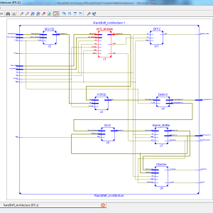
RandShift: An Energy-Efficient Fault Tolerant Method in Secure Nonvolatile Main Memory
Abstract:
In this article, we present a simple, yet energy- and area-efficient method for tolerating the stuck-at faults caused by an endurance issue in secure-resistive main memories. In the proposed method, by employing the random characteristics of the encrypted data encoded by the Advanced Encryption Standard (AES) as well as a rotational shift operation, a large number of memory locations with stuck-at faults could be employed for correctly storing the data. Due to the simple hardware implementation of the proposed method, its energy consumption is considerably smaller than that of other recently proposed methods. The technique may be employed along with other error correction methods, including the error correction code (ECC) and the error correction pointer (ECP). To assess the efficacy of the proposed method, it is implemented in a phase-change memory (PCM)- based main memory system and compared with three error tolerating methods. The results reveal that for a stuck-at fault occurrence rate of 10−2 and with the uncorrected bit error rate of 2 × 10⁻³, the proposed method achieves 82% energy reduction compared to the state-of-the-art method. More generally, using a simulation analysis technique, we show that the fault coverage of the proposed method is similar to that of the state-of-the-art method.
List of the following materials will be included with the Downloaded Backup: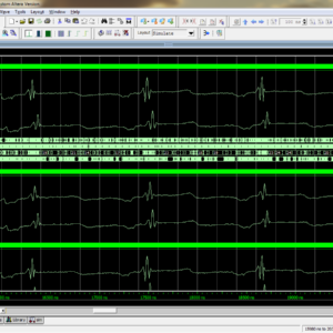
Sparse FIR Filter Design via Partial 1-Norm Optimization
Abstract:
Electrocardiogram (ECG) is a form of cardiovascular measurement, for the diagnosis of different heart rate conditions. However, numerous noises usually harm the amplitude and time period of the signal from the ECG signal, at following a transition of the analog ECG signal from the sensor module into a digital format. The appropriate digital filter may be used to remove different forms of noise such as Baseline Wander, Power line interference, High frequency noise and Physiological Artifacts. The Digital FIR filter will have prospected to reduced the artifacts in the ECG signals. The signals taken from the MIT-BIH data base which contains the normal and abnormal waveforms. This Digital FIR filter can have more performance by using more TAP numbers such as multiplying, delaying and getting more effectiveness. This proposed work would implement a 1 norm minimization in the FIR filter with liner step method to minimize sparse complexity and reduce the mini-max approximation error for sparse maximization. Given these facts, several rules for selecting indicators of potential zero coefficients to be used in 1 standard optimization are adopted in the proposed algorithm. The efficacy of the proposed design algorithm was developed in Verilog HDL, simulated in Modelsim software and synthesized in Xilinx vertex 5 FPGA, and finally prove all the parameters in terms of area, delay and power.
List of the following materials will be included with the Downloaded Backup: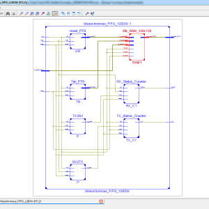
The Mesochronous Dual-Clock FIFO Buffer
Abstract:
To increase system composability and facilitate timing closure, fully synchronous clocking is replaced by more relaxed clocking schemes, such as mesochronous clocking. Under this regime, the modules at the two ends of a mesochronous interface receive the same clock signal, thus operating under the same clock frequency, but the edges of the arriving clock signals may exhibit an unknown phase relationship. In such cases, clock synchronization is needed when sending data across modules. In this brief, we present a novel mesochronous dual-clock first-input– first-output (FIFO) buffer that can handle both clock synchronization and temporary data storage, by synchronizing data implicitly through the explicit synchronization of only the flow-control signals. The proposed design can operate correctly even when the transmitter and the receiver are separated by a long link whose delay cannot fit within the target operating frequency. In such scenarios, the proposed mesochronous FIFO can be extended to support multicycle link delays in a modular manner and with minimal modifications to the baseline architecture. When compared with the other state-of-the-art dual-clock mesochronous FIFO designs, the new architecture is demonstrated to yield a substantially lower cost implementation.
List of the following materials will be included with the Downloaded Backup:
Vital-Sign Processing Receiver With Clutter Elimination Using Servo Feedback Loop for UWB Pulse Radar System
Abstract:
This brief presents a vital-sign processing circuit for simultaneous dc/near-dc elimination and out-of-band interference rejection without any digital signal processing or algorithm assistance for the ultra wideband (UWB) pulse-based radar system. An intrinsic self balanced MOS diode (SBMD) was proposed as a stable and balanced pseudo resistor applied under a servo feedback loop in a vital-sign receiver of the sensing radar to perform as a high-pass filter (HPF) with an ultralow corner frequency lower than 0.5 Hz for removing undesired clutters of the reflected signals and input dc-offset voltages from innate circuit offsets. A third-order switched-capacitor (SC) Chebyshev low-pass filter (LPF) with leap-frog topology as the subsequent stage was adopted to suppress the out-band noises, thereby establishing an integrated vital-sign processing circuit with band pass frequency response and incorporating it into a radar module to verify its viability.
List of the following materials will be included with the Downloaded Backup:IEEE Transactions on VLSI, VLSI IEEE Project, VLSI Low Power Project, VLSI High Speed Project, VLSI Area Efficient Project, Low Cost VLSI Projects, High Speed VLSI Design projects ( CDMA, RTOS, DSP, RF, IF, etc), Low Power VLSI Design projects, Area Efficient VLSI Design projects , Audio processing VLSI Design projects, Signal Processing VLSI Design projects, Image Processing VLSI Design projects, Backend VLSI Design projects ( CMOS, TFET, BisFET, FeFET, etc), Timing & Delay Reduction VLSI Projects, Internet of Things VLSI Projects, Testing, Reliability and Fault Tolerance VLSI Projects, VLSI Applications ( Communicational, Video, Security, Sensor Networks, etc), SOC VLSI Projects, Network on Chip VLSI Projects, Wireless Communication VLSI Projects, VLSI Verifications Projects ( UVM, OVM, VVM, System Verilog.
Provide Wordlwide Online Support
We can provide Online Support Wordlwide, with proper execution, explanation and additionally provide explanation video file for execution and explanations.
24/7 Support Center
NXFEE, will Provide on 24x7 Online Support, You can call or text at +91 9789443203, or email us nxfee.innovation@gmail.com
Terms & Conditions:
Customer are advice to watch the project video file output, and before the payment to test the requirement, correction will be applicable.
After payment, if any correction in the Project is accepted, but requirement changes is applicable with updated charges based upon the requirement.
After payment the student having doubts, correction, software error, hardware errors, coding doubts are accepted.
Online support will not be given more than 3 times.
On first time explanation we can provide completely with video file support, other 2 we can provide doubt clarifications only.
If any Issue on Software license / System Error we can support and rectify that within end of day.
Extra Charges For duplicate bill copy. Bill must be paid in full, No part payment will be accepted.
After payment, to must send the payment receipt to our email id.
Powered by NXFEE INNOVATION, Pondicherry.
Call us today at : +91 9789443203 or Email us at nxfee.innovation@gmail.com
NXFEE Development & Services

Product Categories
- 2014 (11)
- 2015 (39)
- 2016 (30)
- 2017 (16)
- 2018 (17)
- 2019 (42)
- 2020 (29)
- 2021 (17)
- 2022 (23)
- Accessories (45)
- Area Efficient (117)
- High speed VLSI Design (56)
- IEEE (15)
- Image Processing (40)
- Low power VLSI Design (98)
- NOC VLSI Design (2)
- VLSI (251)
- VLSI 2023 (21)
- VLSI 2024 (18)
- VLSI 2025 (31)
- VLSI 2026 (4)
- VLSI Application / Interface and Mini Projects (31)
- VLSI_2023 (15)
Filter by price
Product Status
Sort by producents

Copyright © 2026 Nxfee Innovation.