218 Products found
VLSI Implementation of an Edge-Oriented Image Scaling Processor
Abstract:
Image scaling is a very important technique and has been widely used in many image processing applications. In this paper, we present an edge-oriented area-pixel scaling processor. To achieve the goal of low cost, the area-pixel scaling technique is implemented with a low-complexity VLSI architecture in our design. A simple edge catching technique is adopted to preserve the image edge features effectively so as to achieve better image quality. Compared with the previous low-complexity techniques, our method performs better in terms of both quantitative evaluation and visual quality. The seven-stage VLSI architecture of our image scaling processor contains 10.4-K gate counts and yields a processing rate of about 200 MHz by using TSMC 0.18- m technology.
List of the following materials will be included with the Downloaded Backup:
Design of Power and Area Efficient Approximate Multipliers
Abstract:
Approximate computing can decrease the design complexity with an increase in performance and power efficiency for error resilient applications. This brief deals with a new design approach for approximation of multipliers. The partial products of the multiplier are altered to introduce varying probability terms. Logic complexity of approximation is varied for the accumulation of altered partial products based on their probability. The proposed approximation is utilized in two variants of 16-bit multipliers. Synthesis results reveal that two proposed multipliers achieve power savings of 72% and 38%, respectively, compared to an exact multiplier. They have better precision when compared to existing approximate multipliers. Mean relative error figures are as low as 7.6% and 0.02% for the proposed approximate multipliers, which are better than the previous works. Performance of the proposed multipliers is evaluated with an image processing application, where one of the proposed models achieves the highest peak signal to noise ratio.
List of the following materials will be included with the Downloaded Backup:
Low Power Split Radix FFT Processors Using Radix 2 Butterfly Units
Split radix fast Fourier Transform (SRFFT) is an ideal candidate for the implementation of a low power FFT processor, because it has the lowest number of arithmetic operation among all the FFT algorithms. In the design of such processors, an efficient addressing scheme for FFT data as well as twiddle factors is required. The signal flow graph of SRFFT is the same as radix-2 FFT, and therefore, the conventional address generation schemes of FFT data could also be applied to SRFFT. However SRFFT has irregular locations of twiddle factors and forbids the application of radix-2 address generation methods. This brief presents a shared memory low power SRFFT processor architecture. The SRFFT can be computed by using a modified radix-2 butterfly unit. The butterfly unit exploits the multiplier-gating technique to save dynamic power at the expense of using more hardware resources. In addition, two novel address generation algorithm for both the trivial and nontrivial twiddle factors are developed. In this paper We increases the architecture size, of radix-4 and 2048 point complex valued transform, and shown the performance of area, power and delay, and synthesized xilinx FPGA on s6lx16-2csg225.
List of the following materials will be included with the Downloaded Backup:
RF Power Gating A Low Power Technique for Adaptive Radios
Low Power System for Detection of Symptomatic Patterns in Audio Biological Signals
We present a low-power, efficacious, and scalable system for the detection of symptomatic patterns in biological audio signals. The digital audio recordings of various symptoms, such as cough, sneeze, and so on, are spectrally analyzed using a discrete wavelet transform. Subsequently, we use simple mathematical metrics, such as energy, quasi-average, and coastline parameter for various wavelet coefficients of interest depending on the type of pattern to be detected. Furthermore, a mel-frequency cepstrum-based analysis is applied to distinguish between signals, such as cough and sneeze, which have a similar frequency response and, hence, occur in common wavelet coefficients. Algorithm-circuit codesign methodology is utilized in order to optimize the system at algorithm and circuit levels of design abstraction. This helps in implementing a low-power system as well as maintaining the efficacy of detection. The system is scalable in terms of user specificity as well as the type of signal to be analyzed for an audio symptomatic pattern. The proposed architecture of this paper analysis the logic size, area and power consumption using Xilinx 14.2.
List of the following materials will be included with the Downloaded Backup:
Low Power FPGA Design Using Memoization Based Approximate Computing
Field-programmable gate arrays (FPGAs) are increasingly used as the computing platform for fast and energy efficient execution of recognition, mining, and search applications. Approximate computing is one promising method for achieving energy efficiency. Compared with most prior works on approximate computing, which target approximate processors and arithmetic blocks, this paper presents an approximate computing methodology for FPGA-based design. It studies memoization as a method for approximation on FPGA and analyzes different architectural and design parameters that should be considered. The proposed design flow leverages on high-level synthesis to enable memoization-based microarchitecture generation, thus also facilitating a C-to-register-transfer-level synthesis. When compared with the previous approaches of bit-width truncation and approximate multipliers, memoization-based approximate computation on FPGA achieves a significant dynamic power saving (around 20%) with very small area overhead (<5%) and better power-to-signal noise ratio values for the studied image processing benchmarks. The proposed architecture of this paper is verified using vivado HLS..
List of the following materials will be included with the Downloaded Backup:
An Efficient VLSI Architecture of a Reconfigurable Pulse Shaping FIR Interpolation
This brief proposes a two-step optimization technique for designing a reconfigurable VLSI architecture of an interpolation filter for multi-standard digital up converter (DUC) to reduce the power and area consumption. The proposed technique initially reduces the number of multiplications per input sample and additions per input sample by 83% in comparison with individual implementation of each standard’s filter while designing a root-raised-cosine finite-impulse response filter for multi-standard DUC for three different standards. In the next step, a 2-bit binary common sub-expression (BCS)-based BCS elimination algorithm has been proposed to design an efficient constant multiplier, which is the basic element of any filter. This technique has succeeded in reducing the area and power usage by 41% and 38%, respectively, along with 36% improvement in operating frequency over a 3-bit BCS-based technique reported earlier, and can be considered more appropriate for designing the multi-standard DUC. The proposed architecture of this paper analysis the logic size, area and power consumption using Xilinx 14.2.
List of the following materials will be included with the Downloaded Backup:
High Speed Low Power and Highly Reliable Frequency Multiplier for DLL Based Clock Generator
To propose a novel frequency multiplier with high-speed, low-power, and highly reliable design for a delay-locked loop-based clock generator to generate a multiplied clock with a high frequency and wide frequency range. The proposed edge combiner achieves a high-speed and highly reliable operation using a hierarchical structure and an overlap canceller. In addition, by applying the logical effort to the pulse generator and multiplication-ratio control logic design, the proposed frequency multiplier minimizes the delay difference between positive- and negative-edge generation paths, which causes a deterministic jitter. Finally, a numerical analysis is performed to analyze and compare the performance of the proposed frequency multiplier with that of previous frequency multipliers. The proposed frequency multiplier is fabricated using a 0.13-µm CMOS process technology, and has the multiplication ratios of 1, 2, 4, 8, and 16, and an output range of 50 MHz–3.3 GHz. The frequency multiplier achieves power consumption is 17.49mW. The proposed architecture of this paper is analysis the logic size, area and power consumption using tanner tool.
List of the following materials will be included with the Downloaded Backup:
Full Swing Local Bitline SRAM Architecture Based on the 22 nm FinFET Technology for Low Voltage Operation
The previously proposed average-8T static random access memory (SRAM) has a competitive area and does not require a write-back scheme. In the case of an average-8T SRAM architecture, a full-swing local bitline (BL) that is connected to the gate of the read buffer can be achieved with a boosted wordline (WL) voltage. However, in the case of an average-8T SRAM based on an advanced technology, such as a 22-nm FinFET technology, where the variation in threshold voltage is large, the boosted WL voltage cannot be used, because it degrades the read stability of the SRAM. Thus, a full-swing local BL cannot be achieved, and the gate of the read buffer cannot be driven by the full supply voltage (VDD), resulting in a considerably large read delay. To overcome the above disadvantage, in this paper, a differential SRAM architecture with a full-swing local BL is proposed. In the proposed SRAM architecture, full swing of the local BL is ensured by the use of cross-coupled pMOSs, and the gate of the read buffer is driven by a full VDD, without the need for the boosted WL voltage. Various configurations of the proposed SRAM architecture, which stores multiple bits, are analyzed in terms of the minimum operating voltage and area per bit. The proposed SRAM that stores four bits in one block can achieve a minimum voltage of 0.42 V and a read delay that is 62.6 times lesser than that of the average-8T SRAM based on the 22-nm FinFET technology. The proposed architecture of this paper is analysis the area and power consumption using tanner tool.
List of the following materials will be included with the Downloaded Backup:
Fully Reused VLSI Architecture of FM0Manchester Encoding Using SOLS Technique for DSRC Applications
The dedicated short-range communication (DSRC) is an emerging technique to push the intelligent transportation system into our daily life. The DSRC standards generally adopt FM0 and Manchester codes to reach dc-balance, enhancing the signal reliability. Nevertheless, the coding-diversity between the FM0 and Manchester codes seriously limits the potential to design a fully reused VLSI architecture for both. In this paper, the similarity-oriented logic simplification (SOLS) technique is proposed to overcome this limitation. The encoding capability of this paper can fully support the DSRC standards of America, Europe, and Japan. This paper not only develops a fully reused VLSI architecture, but also exhibits an efficient performance compared with the existing works. The proposed architecture of this paper analysis the logic size, area and power consumption using Xilinx 14.2.
List of the following materials will be included with the Downloaded Backup:
A VLSI Architecture for Watermarking of Gray scale Images using Weighted Median Prediction
Abstract:
Watermarking the digital data is a familiar technique to authenticate and resolve the copyright issues of multimedia data. This paper proposes a new VLSI architecture for watermarking grayscale images using weighted median prediction operation, as this mechanism will have a minimum computation complexity. In this VLSI based data hiding process the secret digital signature is hidden in the host image and analyzed with the PSNR value and Payload capacity.
List of the following materials will be included with the Downloaded Backup: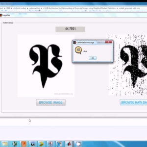
VLSI Implementation of Efficient Image Watermarking Algorithm
Abstract:
The watermarking is the important multimedia content for authentication and security in nowadays. We are proposed to implement the watermarking in FPGA with VLSI architecture. And also use the Haar discrete wallet transform and bit plane slicing for creating the water marking images and extracted watermark images. The area, power, delay of the proposed architecture is analysis using Xilinx 14.2.
List of the following materials will be included with the Downloaded Backup: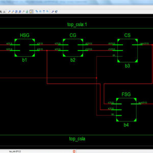
Area Delay Power Efficient Carry Select Adder
Source : VHDL
Abstract:
We are briefly discussing the logic operations are involved in the CSLA (conventional carry select adder) and the square root conventional carry select adder. We have discard the all the extra logic operations present in the conventional CSLA. In the proposed system carry selection is take place in before the final sum calculation. The proposed system achieves the optimization in the logic units. Finally the FPGA synthesis results shows to achieves a design the low power architecture for CSLA.
List of the following materials will be included with the Downloaded Backup:
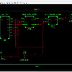
Low Power Compressor Based MAC Architecture for DSP Applications
This paper presents the low power compressor based Multiply-Accumulate (MAC) architecture for DSP applications. In VLSI, highly computed arithmetic cells including adders and multipliers are the most copiously used components. Efficient implementation of arithmetic logic units, floating point units and other dedicated functional components are utilized in most of the microprocessors and digital signal processors (DSPs). Thus in this brief, compressor circuit has been illustrated for the low power applications and also the impact of datapath circuits has been demonstrated. The proposed low power compressor architecture was applied to MAC unit and compared against the conventional compressor based MAC units and observed that the proposed architecture has reduced significant amount of leakage power. The proposed architecture of this paper analysis the logic size, area and power consumption using Xilinx 14.2.
List of the following materials will be included with the Downloaded Backup:
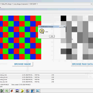
VLSI-Oriented Lossy Image Compression Approach using DA-Based 2D-Discrete Wavelet
We introduced a Discrete Wavelet Transform (DWT) based VLSI-oriented lossy image compression approach, widely used as the core of digital image compression. Here, Distributed Arithmetic (DA) technique is applied to determine the wavelet coefficients, so that the number of arithmetic operation can be reduced substantially. As well, the compression rate is enhanced with the aid of introducing RW block that blocks some of the coefficients obtained from the high pass filter to zero. Subsequently, Differential Pulse-Code Modulation (DPCM) and huffman-encoding are applied to acquire the binary sequence of the image. The proposed architecture of this paper analysis the logic size, area and power consumption using Xilinx 14.2.
List of the following materials will be included with the Downloaded Backup: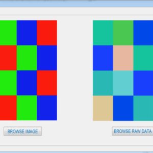
A New Parallel VLSI Architecture for Real-time Electrical Capacitance Tomography
This paper presents a fixed-point reconfigurable parallel VLSI hardware architecture for real-time Electrical Capacitance Tomography (ECT). Another FPGA module performs the inverse steps of the tomography algorithm. A dual port built-in memory banks store the sensitivity matrix, the actual value of the capacitances, and the actual image with RGB format. A two dimensional (2D) core multiprocessing elements (PE) engine intercommunicates with these memory banks via parallel buses. We are focus only on the FPGA module because the design is decide the power consumption and cost. The proposed architecture of this paper analysis the logic size, area and power consumption using Xilinx 14.2. List of the following materials will be included with the Downloaded Backup:
Low-Energy Power-ON-Reset Circuit for Dual Supply SRAM
Design of a low-energy power-ON reset (POR) circuit is proposed to reduce the energy consumed by the stable supply of the dual supply static random access memory (SRAM), as the other supply is ramping up. The proposed POR circuit, when embedded inside dual supply SRAM, removes its ramp-up constraints related to voltage sequencing and pin states. The circuit consumes negligible energy during ramp-up, does not consume dynamic power during operations, and includes hysteresis to improve noise immunity against voltage fluctuations on the power supply. The POR circuit, designed in the 40-nm CMOS technology within 10.6-µm2 area, enabled 27× reduction in the energy consumed by the SRAM array supply during periphery power-up in typical conditions. The proposed architecture of this paper area and power consumption analysis using tanner tool.
List of the following materials will be included with the Downloaded Backup:
Low Power Variation Tolerant Nonvolatile Lookup Table Design
Emerging nonvolatile memories (NVMs), such as MRAM, PRAM, and RRAM, have been widely investigated to replace SRAM as the configuration bits in field-programmable gate arrays (FPGAs) for high security and instant power ON. However, the variations inherent in NVMs and advanced logic process bring reliability issue to FPGAs. This brief introduces a low-power variation-tolerant nonvolatile lookup table (nvLUT) circuit to overcome the reliability issue. Because of large ROFF/RON, 1T1R RRAM cell provides sufficient sense margin as a configuration bit and a reference resistor. A single-stage sense amplifier with voltage clamp is employed to reduce the power and area without impairing the reliability. Matched reference path is proposed to reduce the parasitic RC mismatch for reliable sensing. Evaluation shows that 22% reduction in delay, 38% reduction in power, and the tolerance of variations of 2.5× typical RON or ROFF in reliability are achieved for proposed nvLUT with six inputs. The proposed architecture of this paper area and power consumption analysis using tanner tool.
List of the following materials will be included with the Downloaded Backup:
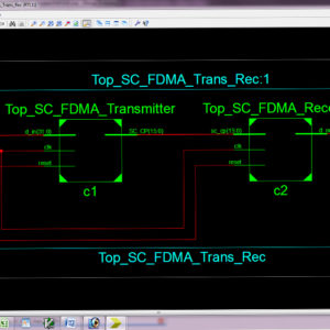
A High-Throughput VLSI Architecture for Hard and Soft SC-FDMA MIMO Detectors
Abstract:
A novel low-complexity multiple-input multiple-output (MIMO) detector tailored for single-carrier frequency division-multiple access (SC-FDMA) systems, suitable for efficient hardware implementations. The proposed detector starts with an initial estimate of the transmitted signal based on a minimum mean square error (MMSE) detector. Subsequently, it recognizes less reliable symbols for which more candidates in the constellation are browsed to improve the initial estimate. The proposed architecture of this paper analysis the logic size, area and power consumption using Xilinx 14.2.
List of the following materials will be included with the Downloaded Backup:
Fully Pipelined Low-Cost and High-Quality Color Demosaicking VLSI Design for Real-Time Video Applications
This system presents a fully pipelined color demosaicking design. To improve the quality of reconstructed images, a linear deviation compensation scheme was created to increase the correlation between the interpolated and neighboring pixels. Furthermore, immediately interpolated green color pixels are first to be used in hardware-oriented color demosaicking algorithms, which efficiently promoted the quality of the reconstructed image. A boundary detector and boundary mirror machine were added to improve the quality of pixels located in boundaries. In addition, a hardware sharing technique was used to reduce the hardware costs of three interpolators. Finally these are implemented and get the simulated result is compared to the previous architecture. The code are simulated and power, area, cost are taken using Xilinx 14.2 software and MATLAB. Compared with the previous low complexity designs, this work has the benefits in terms of low cost, low power consumption, and high performance.
List of the following materials will be included with the Downloaded Backup:
Low-Cost High-Performance VLSI Architecture for Montgomery Modular Multiplication
Source Code : VHDL & VERILOG HDL
Abstract: This paper proposes a simple and efficient Montgomery multiplication algorithm such that the low-costand high-performance Montgomery modular multiplier can be implemented accordingly. The proposed multiplier output data with representation and uses only one parallel prefix adder to avoid a carry propagation and reduce the area, power and delay, and also increasing the speed. Mainly the usage of parallel prefix adder is to reduce the significant delay reduction and area × time2 improvements, all this at the cost of higher power consumption, which is the main reason preventing the use of parallel-prefix adders to achieve high-speed reverse converters in nowadays systems. Hence, to solve the high power consumption problem, novel specific hybrid parallel-prefix-based adder components those provide better trade-off between delay and power consumption. As a result, the extra clock cycles for operand pre-computation and format conversion can be hidden and high throughput can be obtained. Experimental results show that the proposed Montgomery modular multiplier can achieve higher performance and significant area–time product improvement when compared with previous designs. Using VHDL to design the RTL, and the result to be shown in Xilinx 14.2 with Power consumption and area reduction.
List of the following materials will be included with the Downloaded Backup:
Implementation of High-Precision MFCC Feature Extraction Using FPGA for Speech Recognition
Proposed Abstract:
Speaker recognition is one of the technologies that may be used for biometric identification, and it offers higher application possibilities in many sectors. At the moment, the implementation of the speaker identification algorithm on the hardware is mostly dependent on the SOC of the FPGA. An FPGA-based real-time technique for extracting acoustic characteristics is presented in this research. The method is based on MFCC, which stands for Mel Frequency Cepstral Coefficients. The trials have shown that the FPGA-based MFCC calculation has a high level of accuracy; the purpose of this study is to enhance the performance assessment of MFCC by making use of novelty-based architecture. In this study, a technique for FPGA-based speech recognition is provided. This approach was developed by investigation and analysis of the speaker recognition algorithm. The IFFT, the Mell filter, the DFT, the derivatives, and the Hamming Window with pre-emphasis are every aspect of this approach. This proposed MFCC will be constructed with an AHB interface in order to facilitate higher access DMA Controller when it is used in SOC applications. This work was carried out using Verilog HDL, and it was generated with Xilinx Vivado FPGA. Additionally, all of the parameters were analyzed and compared with regard to area, latency, and power.
List of the following materials will be included with the Downloaded Backup:
Parallel Pipelined Architecture and Algorithm for Matrix Transposition Using Registers
Base Paper Abstract:
In this brief, we present a new algorithm and architecture for continuous-flow matrix transposition using registers. The algorithm supports P-parallel matrix transposition. The hardware architecture reaches the theoretical minimums in terms of latency and memory. It is composed of a group of identical cascaded basic swap circuits, whose stages are determined by the corresponding algorithm, and can be controlled via a set of counters. Compared with the state-of-the-art architecture, the proposed architecture supports matrices whose rows and columns are integer multiples of P. Here P can be arbitrary, including but not limited to power-of-two integers. Moreover, our results provide additional insight into continuous-flow non-square matrix transposition.
List of the following materials will be included with the Downloaded Backup:
A Reversible Processor Architecture and Its Reversible Logic Design
Proposed Abstract:
This paper presents the design and FPGA implementation of a 16-bit reversible processor architecture employing Fredkin, Feynman, and PERES gate architectures for reversible logic design. Reversible computing offers promising advantages in terms of energy efficiency and information loss prevention, making it suitable for various emerging computing paradigms. The proposed processor architecture encompasses a carefully crafted instruction set, data path, and control logic, all realized using reversible logic gates. Key components such as the ALU, register file, and memory elements are designed with an emphasis on reversibility. The design is implemented using Hardware Description Languages (HDLs), targeting a specific FPGA platform. The paper outlines the design methodology, gate-level implementation details, memory design considerations, FPGA synthesis, and testing procedures. Furthermore, it discusses optimization strategies and presents simulation results to validate the functionality and efficiency of the proposed reversible processor architecture. This work contributes to the advancement of reversible computing and provides insights into the practical realization of reversible processor architectures on FPGA platforms.
List of the following materials will be included with the Downloaded Backup:
Design and Analysis of a Majority Logic Based Imprecise 6-2 Compressor for Approximate Multipliers
Base Paper Abstract:
Approximate computing is an emerging paradigm for trading off computing accuracy to reduce energy consumption and design complexity in a variety of applications, for which exact computation is not a critical requirement. Different from conventional designs using AND-OR and XOR gates, the majority gate is widely used in many emerging nanotechnologies. An ultra-efficient 6-2 compressor is proposed in this paper. It is composed of two majority gates that lead to low energy consumption and high hardware efficiency. The proposed compressor is utilized in the approximate partial product reduction of a modified 8×8 Dadda multiplier with a truncated structure. Experimental results show that this multiplier realizes a significant reduction in hardware cost, especially in terms of power and area, on average by up to 40% and 31% respectively, compared to exact and state-of-the-art designs. The application of image multiplication is also presented to assess the practicability of the multiplier. The results show that the proposed multiplier results in images with higher quality in peak signal to noise ratio (PSNR) and mean structural similarity index metric (MSSIM) compared to other designs.
List of the following materials will be included with the Downloaded Backup:
Fast and Hardware-Efficient Variable Step Size Adaptive Beamformer
Base Paper Abstract:
Constant step size least mean square (CSS-LMS) is one of the most popular adaptive beamforming algorithms. However, for varying channel signal-to-noise ratios (SNRs), the CSS algorithms are not effective, and there is a need for variable step size (VSS) algorithms. The VSS algorithms provide extremely deep nulls for the interferences; however, they are complex to implement on hardware. Hence, this paper proposes two hardware-efficient variable step size algorithms, namely, efficient variable step size LMS (EVSS-LMS) and reduced complexity parallel LMS (EVSS-RC-pLMS). The proposed EVSS algorithms eliminate the complex operations of VSS algorithms like division and exponential and approximate them to simpler operations. Further, MATLAB simulations demonstrate accelerated convergence, deep nulls, a lower error floor, and better performance in varying SNR environments for the proposed algorithms. Additionally, the finite precision radiation patterns are similar to infinite precision. Hardware synthesis results show the outstanding performance of EVSS in terms of resource utilization on the Xilinx Artix-7 FPGA.
List of the following materials will be included with the Downloaded Backup: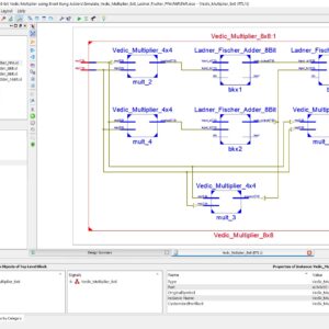
Design of High Speed 8-bit Vedic Multiplier using Brent Kung Parallel Prefix Adder
Base Paper Abstract:
One of the primary purposes of a digital signal processing system is multiplication. The multiplier’s performance affects the DSP system’s overall performance. Therefore, it is crucial to create an effective and quick multiplier implementation design. Vedic mathematics can be used to simplify complex computations so that they are easier to perform verbally. Urdhva Triyambakam is the multiplication algorithm used in Vedic math. In this paper, we employing Brent Kung adder to enhance the Vedic multiplier’s performance. The Urdhva Tiryagbhyam sutra is being used in place of other multiplication strategies since it applies to all instances of algorithms for N x N bit numbers and produces the least amount of latency. Four 4-bit vedic multipliers, two 8-bit Brent Kung adders, one 4-bit Brent Kung adder, and an OR gate are used to create an 8-bit vedic multiplier. A 4-bit vedic multiplier is created similarly by combining four 2-bit vedic multipliers, two 4-bit Brent Kung Adders, one 2-bit Brent Kung Adder, and one OR gate. These four-bit vedic multipliers are then combined to form an eight-bit vedic multiplier. After that, Xilinx Vivado Software is used to simulate and synthesis the 8 x 8 Vedic Multiplier, which was coded in Verilog HDL. The proposed Vedic Multiplier is outperformed in terms of speed when compared to related works.
List of the following materials will be included with the Downloaded Backup:
Design and Implementation of an 8-bit Approximate Wallace Tree Multiplier for Energy Efficient Deep Neural Networks
Base Paper Abstract:
Approximate arithmetic computing circuits and architectures have been proven to be energy efficient designs for Deep Neural Networks (DNNs) which are error resilient. In this paper, an approximate 8-bit Wallace Multiplier has been proposed and designed in 90nm CMOS technology for energy efficiency. The proposed 8-bit approximate multiplier design consumes ~32% less energy in comparison to an accurate 8-bit Wallace Tree multiplier with less than 20% Mean Relative Error (MRE).
List of the following materials will be included with the Downloaded Backup: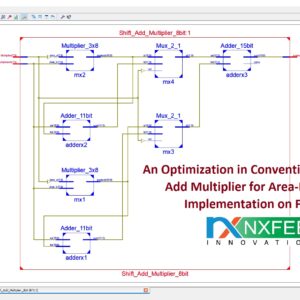
An Optimization in Conventional Shift &Add Multiplier for Area-Efficient Implementation on FPGA
Base Paper Abstract:
FPGA is familiar with prototyping and implementing simple to complex DSP systems. The FPGA based design may be highly affected by factors that include selection of an FPGA board, Electronic Design Automation Tool and the Programming Techniques to optimize the algorithm. The algorithm optimization results in a more compact design regarding the area and achieved frequency. In DSP algorithms optimization, the major bottleneck is the multiplier complexity evident in, for example - FIR, IIR, FFT, and others. Research shows much work on multiplier optimization. Despite all possible optimization techniques, the multiplier consumes tremendous resources when translated on hardware, with more power consumption and observed delay. The proposed work is novel in that it brings resources optimization in a familiar shift and add multiplier algorithm by implementing the design in FPGA and comparing the results with the existing shift, and add a multiplier. In the implementation of the design, Xilinx Vertex -7 FPGA is used along with ISE 14.2 simulators. The parameters to compare are the Lookup tables (Logic element of FPGA), adder/subtractors and the multiplexers, along with performance characters, like the operating frequency, delay and total levels of logic (path travelled by the signal in register transfer level). The output shows that the anticipated design is an excellent alternative to the conventional shift and add algorithm.
List of the following materials will be included with the Downloaded Backup: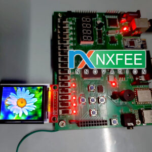
FPGA Implementation of TFT 1.8 inch SPI 128×160 Display ROM Interface
Simple Description:
This ST7735R is a display controller used in small TFT (Thin-Film Transistor) LCD displays. It is often used in combination with microcontrollers or FPGAs to drive these displays. The controller supports the Serial Peripheral Interface mode of communication for sending commands and data to the display. This TFT display helps with a greater number of image and video processing applications. Here we have implemented this TFT display in FPGA hardware implementation using Verilog HDL with a novelty-based architecture design. Finally shown the output with TFT Display.
List of the following materials will be included with the Downloaded Backup:
FPGA Implementation of Spread Spectrum Clock Generator with Onion Modulation
Proposed Abstract:
A Spread Spectrum Clock Generator (SSCG) is used in electronics to purposefully vary the frequency of a clock signal via modulation. Modulation is accomplished by dispersing the energy of the signal throughout a spectrum of frequencies rather than focusing it on a certain frequency. The main objective of using the spread spectrum approach in clock generation is to minimize electromagnetic interference (EMI) and enhance electromagnetic compatibility (EMC) in electronic systems. The main reason for using many layers of modulation in spread spectrum clock production, regardless of whether the name "Onion Modulation" is used, is to provide a more advanced and adaptable method for reducing electromagnetic interference. The primary design feature of the onion wave is that the core portion of the waveform has the least steep slope, which serves to generate the output. In order to optimize the frequency effect design, the conventional approach involves using a memory ROM to regulate the slope and obtain the desired onion waveform. This current methodology necessitates substantial memory allocation and an intricate architecture, resulting in higher power consumption. The proposed method presents a unique architecture for onion modulation, which offers reduced logic size and power usage. This architecture was created using Verilog HDL, tested using Modelsim, and implemented using the Xilinx Vertex-5 FPGA.
List of the following materials will be included with the Downloaded Backup: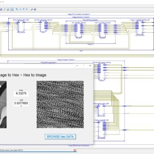
An Efficient Image Encryption Algorithm Based on Innovative DES Structure and Hyperchaotic Keys
Base Paper Abstract:
In fact, as a traditional encryption method, DES has been certified as an unsuitable tool for ciphering due to its smaller key space. Further, in concern of the real-time encryption in the current fast communication era, such as 5G, long-time as well as large computational level processes are not gotten into the consideration. As a result, an innovative encryption structure with hyperchaotic keys for efficient encryption is constructed, where the frame of DES structure is applied, the plain image is shuffled through row and column directions in the first round, and then rearranged to be 64 blocks to fit into the frame of DES structure for 4 rounds ciphering with hyperchaotic subkeys. Also, in order to encrypt the content of the image at the block level, a set of alternative S-box has been produced in this article as well. The simulation results indicate that the proposed scheme is feasible and reliable for digital image encrypting, not only a large key space can be obtained, but also the low correlation of the adjacent contents can be achieved, and further, in comparison of several existing approaches, less-computational resource can be proven as well. In particular, due to the innovative DES structure, the computational speed is significantly faster than the original DES algorithm and many other chaos-based image ciphering schemes.
List of the following materials will be included with the Downloaded Backup:An Innovative Area Efficient Pixel Shuffling Method for Image Encryption Algorithm
Proposed Abstract:
In image processing and computer vision, pixel shuffling is a method used to increase an image's resolution without adding more parameters or network complexity. With this technique, a low-quality image's pixels are rearranged to produce an output with a better resolution. Pixel shuffling has proven successful in a number of applications, such as image synthesis, super-resolution, and style transfer. Its simplicity and efficiency make it an attractive option for tasks where increasing image resolution is essential, while avoiding the computational overhead associated with more complex architectures. The image line buffer based pixel shuffling technique presented in this study is an alternative to the classic method, which takes up more logic space in VLSI implementations. This proposed method splits and reconstructs the source photos using a 5x5 image line buffer. With the use of block interleave techniques, this pixel shuffling approach handled row and column sequence using this 5x5 picture line buffer. In conclusion, this study was compared with the PSNR and SSIM value; comparisons of logic sizes for area, latency, and power were also examined.
List of the following materials will be included with the Downloaded Backup:
FPGA Implementation of 64 Block Data Encryption Standard Algorithm
Proposed Abstract:
The Data Encryption Standard (DES) is widely recognized as the inaugural and prevailing symmetric key method used for the cryptographic processes of encrypting and decrypting digital data. Despite its lack of security against determined attackers in contemporary times, the use of this method persists in older systems. This work introduces a novel implementation of the Data Encryption and Decryption Standard algorithm using Field Programming Gate Arrays (FPGAs) that prioritizes security, high throughput, and space efficiency. The suggested solution involves the creation of a system that utilizes a block size of 64 bits and a key length that is also 64 bits. Additionally, the system operates with a data width of 64 bits. This achievement is accomplished by integrating the notion of pipelining with time variable permutations, and then comparing it with previously shown encryption techniques. The permutations undergo temporal variations under the control of the cryptographer. Hence, the cipher text also undergoes alteration while the key and plaintext remain constant. The algorithm under consideration has been successfully executed on the Xilinx Vetex-5 Field-Programmable Gate Array (FPGA) platform. The findings of this study indicate that the suggested implementation exhibits exceptional speed in comparison to other hardware implementations. Additionally, it demonstrates superior area efficiency and significantly enhanced security measures.
List of the following materials will be included with the Downloaded Backup: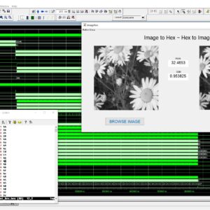
FPGA Implementation of Image Line Buffer to Split and reconstruct a 3×3 size of image pixel with using FIFO Design
Proposed Abstract:
Image line buffers are used in several kinds of image processing applications, particularly where operations must be executed on a per-line basis in order to optimize efficiency. There are many typical applications associated with this technology, including real-time video processing, image filtering, edge detection, computer vision, memory optimization, parallel processing, compression algorithms, and medical imaging. In the context of image and video processing applications, the use of image line buffers may contribute to the optimization of operations when dealing with a continuous stream of frames processed in real time. In the context of image processing, convolutional processes are often used for tasks like as image filtering and blurring. These operations are typically carried out on a per-pixel basis, wherein the value assigned to each pixel is determined by the values of its adjacent pixels. The proposed structure was created using a First-In-First-Out (FIFO) based approach, aiming to decrease the number of logic sizes and complexity in Very Large Scale Integration (VLSI) design architecture. The conversion of design images to hexadecimal and hexadecimal to image format is accomplished using MATLAB GUI applications. These applications also facilitate the comparison of Peak Signal-to-Noise Ratio (PSNR) and Structural Similarity Index Measure (SSIM) values. The internal architecture of the system is implemented using Verilog Hardware Description Language (HDL). Additionally, the simulation is conducted using Modelsim. Furthermore, the system's performance parameters, including area, delay, and power consumption, are compared with those of the Xilinx Vertex-5 Field Programmable Gate Array (FPGA).
List of the following materials will be included with the Downloaded Backup:
Toward the Multiple Constant Multiplication at Minimal Hardware Cost
Base Paper Abstract:
Multiple Constant Multiplication (MCM) over integers is a frequent operation arising in embedded systems that require highly optimized hardware. An efficient way is to replace costly generic multiplication by bit-shifts and additions, i. e. a multiplier less circuit. In this work, we improve the state of-the-art optimal approach for MCM, based on Integer Linear Programming (ILP). We introduce a new low-level hardware cost metric, which counts the number of one-bit adders and demonstrate that it is strongly correlated with the LUT count. This new model permitted us to consider intermediate truncations that permit to significantly save resources when a full output precision is not required. We incorporate the error propagation rules into our ILP model to guarantee a user-given error bound on the MCM results. The proposed ILP models for multiple flavors of MCM are implemented as an open-source tool and, combined with an automatic code generator, provide a complete coefficient-to-VHDL flow. We evaluate our models in extensive experiments, and propose an in-depth analysis of the impact that design metrics have on synthesized hardware.
List of the following materials will be included with the Downloaded Backup:
FPGA Implementation of Single Precision Floating Point Multiplier using High Speed Parallel Prefix Adder based Wallace Tree Multiplier
Base Paper Abstract:
In this paper present, an efficient implementation of single precision method of floating point multiplier target for Xilinx Vertex 5 FPGA using Verilog HDL. The floating point implementation will cover up with 23-bit exponent, 8-bit mantissa, and 1 sign bit. This proposed architecture implement with high speed parallel prefix adder based Wallace Tree Multiplier. a Wallace tree multiplication will provide effective terms of low logic sizes and more speed of operations. In a recent arithmetic applications based circuit design will have more demand with high speed and low area, in this manner the proposed approach of this work will improve the speed of Wallace tree multiplier using 4:2 compressor method without degrading its area parameter. Thus, the proposed method will integrate more efficient and more reliable Kogge stone parallel prefix, Brent kung parallel prefix, Sklansky parallel prefix addition operation in the Wallace tree multiplication on final addition stage at 16-bit data width. Finally, done this floating point multiplier architecture with Wallace tree architecture included normalized rounding method and to reduce area, delay and power. The error difference will have analyzed using Modelsim Software, and analyses optimized logic size's, delay and power consumptions.
List of the following materials will be included with the Downloaded Backup:
Hybrid Protection of Digital FIR Filters
Base Paper Abstract:
A digital finite impulse response (FIR) filter is a ubiquitous block in digital signal processing applications and its behavior is determined by its coefficients. To protect filter coefficients from an adversary, efficient obfuscation techniques have been proposed, either by hiding them behind decoys or replacing them by key bits. In this article, we initially introduce a query attack that can discover the secret key of such obfuscated FIR filters, which could not be broken by the existing prominent attacks. Then, we propose a first of its kind hybrid technique, including both hardware obfuscation and logic locking using a point function for the protection of parallel direct and transposed forms of digital FIR filters. Experimental results show that the hybrid protection technique can lead to FIR filters with higher security while maintaining the hardware complexity competitive or superior to those locked by prominent logic locking methods. It is also shown that the protected multiplier blocks and FIR filters are resilient to existing attacks. The results on different forms and realizations of FIR filters show that the parallel direct form FIR filter has a promising potential for a secure design.
List of the following materials will be included with the Downloaded Backup:
Smart Intelligent and Adaptive Traffic Controller using FPGA
Proposed Abstract:
Traffic management is a critical aspect of modern urban infrastructure, and the ever-increasing volume of vehicles on the road demands innovative and adaptive solutions. This work presents a novel approach to traffic control using Field-Programmable Gate Arrays (FPGAs) as the core technology. The proposed system leverages the capabilities of FPGAs to create a Smart, Intelligent, and Adaptive Traffic Controller that can revolutionize urban traffic management. One of the key features of the proposed work is its adaptability. The system can dynamically adjust traffic signal timings and lane allocations in response to changing traffic patterns of 4-way road conditions with the help of sensor inputs. This methodology adaptability enhances road safety and minimizes traffic delays. The use of FPGA technology in the Traffic controller provides several advantages, including high computational performance, low power consumption, and the ability to reconfigure the system as traffic management needs evolve. Additionally, the system is highly scalable and can be deployed in various urban settings.
List of the following materials will be included with the Downloaded Backup: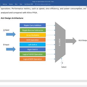
Design and Implementation of Arithmetic Logic Unit in HDL
Proposed Abstract:
Arithmetic logic unit (ALU) is an important part of all digital gadgets and applications. This paper presents the design and implementation of an 8-bit Arithmetic Logic Unit (ALU) with a capability to perform eight distinct operations. ALUs are fundamental components in the central processing units (CPUs) of microprocessors and are responsible for executing arithmetic and logical operations. The primary objective of this research is to design an efficient and versatile 8-bit ALU that can execute a wide range of operations while optimizing for performance and area efficiency. The proposed 8-bit ALU is designed to perform the following eight operations: Ripple carry addition, Ripple borrow subtraction, Array multiplication, XOR operation, left shift, right shift, NAND operation and a logical NOR operation. The research presents a detailed description of the ALU's architecture, its constituent components, and the control mechanism for selecting operations. Performance metrics, such as speed, area efficiency, and power consumption, are analyzed and compared with Xilinx FPGA.
List of the following materials will be included with the Downloaded Backup:
Efficient Design of Behavioral Clock Divider for Multiple Frequency
Proposed Abstract:
Frequency dividers are of utmost importance in frequency synthesizers that are based on phase locked loops. The use of dual modulus presales enhances the versatility of the design in both integer and Fractional-N frequency synthesizers. The selection of an acceptable division ratio is dependent upon the channel spacing and frequency range of the synthesizer. There are several techniques for division in electronic systems, including the injection locked frequency divider (ILFD), complementary ILFDs, flip flop based dividers, dual modulus dividers, and modular dividers. Therefore, these approaches possess some advantages and disadvantages, such as reduced jitter, a restricted frequency tuning range, increased circuit size due to the addition of an LC tank circuit, increased power consumption, and lower quality factor. This work aims at addressing certain issues pertaining to clock dividers and proposes a unique design that utilizes a multiple digital frequency divider based on D flip flops. The architectural design is predicated on the use of a phase shifting mechanism using a D flip flop, which effectively controls the division ratio. The present study involves the use of a preliminary phase shifting melody in conjunction with the Digital Clock Manager (DCM). The auto tuning strategy described in this study aims to adjust the phase difference between two differential clock signals. By intentionally inducing metastability in one or more flip flops, the proposed approach utilizes a digital clock manager in a clock divider to mitigate the effects of metastability and reduce jitter across multiple tuning frequencies. Furthermore, it is worth noting that the logic size and power consumption required for its operation are significantly reduced.
List of the following materials will be included with the Downloaded Backup: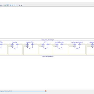
FPGA Heart Rate Monitoring (Pre Processing – QRS Detection Stage)
Base Paper Abstract:
The continuous monitoring of cardiac patients requires an ambulatory system that can automatically detect heart diseases. This study presents a new field programmable gate array (FPGA)-based hardware implementation of the QRS complex detection. The proposed detection system is mainly based on the Pan and Tompkins algorithm, but applying a new, simple, and efficient technique in the detection stage. The new method is based on the centered derivative and the intermediate value theorem, to locate the QRS peaks. The proposed architecture has been implemented on FPGA using the Xilinx System Generator for digital signal processor and the Nexys-4 FPGA evaluation kit. To evaluate the effectiveness of the proposed system, a comparative study has been performed between the resulting performances and those obtained with existing QRS detection systems, in terms of reliability, execution time, and FPGA resources estimation. The proposed architecture has been validated using the 48 half-hours of records obtained from the Massachusetts Institute of Technology - Beth Israel Hospital (MITBIH) arrhythmia database. It has also been validated in real time via the analogue discovery device.
List of the following materials will be included with the Downloaded Backup:
Design of Approximate Restoring Divider
Proposed Abstract:
Approximate computing is an emerging paradigm in error-tolerant applications that leads to power-efficient designs without significant loss in quality. The divider in these applications have complex hardware and more latency among the computational blocks resulting in power consumption. Hence approximating the division module would lead to designs with vastly improved power efficiency. A new approximate subtractor (AxSUB) is proposed in this paper with the intent to reduce the hardware complexity while achieving accuracy within permissible limits. The proposed AxSUB and existing approximate subtractor units are used in the restoring array division (RAD) architecture to prove the efficacy of the AxSUB. This proposed architecture design with 8/4 approximate divider using Verilog HDL and synthesized using Xilinx Spartan 6 FPGA, and proved the performance of area, delay and power.
List of the following materials will be included with the Downloaded Backup: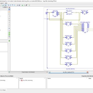
Hamming based Single Fault Error Correction Code
Proposed Abstract:
Signal processing and communication systems often use digital filters. In certain circumstances, the dependability of such systems is essential, prompting the construction of fault-tolerant filters. Many methods that take use of the structure and characteristics of the filters to achieve fault tolerance have been put forward throughout the years. Technology advances permit more intricate systems with several filters. It is typical for some of the filters in such complicated systems to function in simultaneously, for instance by using the same filter on several input signals. Recently, a straightforward method for achieving fault tolerance was given that takes use of the existence of parallel filters. This paper expands on that concept to demonstrate how error correction codes (ECCs), in which each filter is the equivalent of a bit in a conventional ECC, may be used to secure parallel filters. When there are several parallel filters operating simultaneously, this new technique enables more effective protection. The efficiency of the method in terms of protection and implementation cost is assessed using a case study of parallel finite impulse response filters.
List of the following materials will be included with the Downloaded Backup:
FPGA Implementation of High Performance Reversible logic based 16×16 Array Multiplier
Proposed Abstract:
In this recent technology of digital gadgets and digital signal processing and image processing method will have more priority in arithmetic operation, such as multiplication, divisions, addition and subtractions. In this operations of arithmetic unit will have number of garbage signal with more memory logic element, due to this problem these arithmetic operations will take more area, delay and power in VLSI system design. Here, this proposed work will present a arithmetic operation using reversible logic method, thus it take memory less logic and less garbage elements, therefore here this reversible logic method will integrated using reversible half adders and full adder in array multiplier and proved the performance with less garbage signals. Finally, this work will have integrated in Verilog HDL, simulated in Modelsim and Synthesized in Xilinx FPGA, and also compared all the parameter in terms of area, delay and power.
List of the following materials will be included with the Downloaded Backup: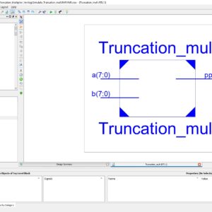
FPGA Implementation of 8×8 Truncated Multiplier
Proposed Abstract:
The operation of multiplication is an often encountered need in the field of digital signal processing. Parallel multipliers provide a rapid approach for performing multiplication operations, while demanding a significant amount of space in VLSI (Very Large Scale Integration) implementations. In the majority of signal processing applications, there is a preference for using a rounded result in order to prevent an increase in the size of the word. Therefore, an important goal in the design process is to minimize the spatial demand of the rounded output multiplier. This study introduces a novel approach to parallel multiplication that efficiently calculates the products of two n-bit values by selectively summing the most important columns using a variable correction technique. This research furthermore includes a comparative analysis of the implementation of 8X8 conventional and truncated multipliers using Verilog Hardware Description Language (HDL) on Field Programmable Gate Arrays (FPGAs). The shortened multiplier demonstrates a much greater decrease in device consumption as compared to the regular multiplier. A conventional multiplier performs computations on n x n bits and produces a weighted sum of the output, consisting of 2n bits. In contrast, a truncated multiplier generates an output of just n bits from the n x n bit input. The use of logic gates in both internal and external hardware design will be decreased. Truncated multipliers provide a viable approach for achieving significant reductions in FPGA resources, latency, and power consumption compared to regular parallel multipliers, particularly in scenarios where the complete accuracy provided by the standard multiplier is unnecessary.
List of the following materials will be included with the Downloaded Backup: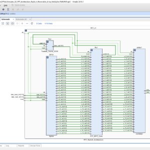
Design of SEU Tolerant 2D-FFT in SRAM-based FPGA
Base Paper Abstract:
2-Dimensional fast Fourier transform (FFT) has been widely used in radar signal process. Due to the need for high performance, field programmable gate array (FPGA) is an ideal hardware device for this application. For space-borne radar platform such as synthetic aperture radar (SAR), single-event upsets (SEUs) can cause lots of soft errors in static random access memory (SRAM) based FPGA. As to this, protecting the 2D-FFT implemented in FPGA from SEUs is very important. In this article, we analyze the critical weakness induced by SEUs in the 2D-FFT process, and then a 2D-FFT design with high SEU resilience is presented. The design utilizes the advantage of several anti-SEU methods. For butterfly control in FFT, partially triple modular redundancy (TMR) is used. For data buffers, error correction code (ECC) is applied to read and write operation. Furthermore, safe finite state machine (FSM) is adopted by important control registers. Fault injection results show that all these reinforcement technologies contribute to enhance the ability to mitigate the SEU effects.
List of the following materials will be included with the Downloaded Backup: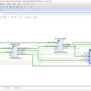
FPGA Implementation of D8PSK Demodulator
Base Paper Abstract:
Differential phase shift keying (DPSK) is a modulation scheme that facilitates non coherent demodulation and is employed for various applications such as Wireless Local Area Networks (WLANs), Bluetooth and RFID communication. In this paper, design, development and hardware implementation of a new demapping scheme for Differential 8-PSK (D8PSK) demodulator on a Zynq 7000 FPGA based ZED board is proposed using the concepts of model based design. The proposed work can be easily extended to other M-ary DPSK schemes.
List of the following materials will be included with the Downloaded Backup:
A Lightweight True Random Number Generator for Root of Trust Applications
Base Paper Abstract:
There are many schemes proposed to protect integrated circuits (ICs) against an unauthorized access and usage, or at least to mitigate security risks. They lay foundations for hardware roots of trust whose crucial security primitives are generators of truly random numbers. In particular, such generators are used to yield one-time challenges (nonces) supporting the IC authentication protocols employed to counteract potential threats such as untrusted users accessing ICs. However, IC vendors raise several concerns regarding the complexity of these solutions, both in terms of area overhead, the impact on the design flow, and testability. These concerns have motivated this work presenting a simple, yet effective, all-digital lightweight and self-testable random number generator to produce a nonce. It builds on a generic ring generator architecture, i.e., an area and time optimized version of a linear feedback shift register, driven by a multiple-output ring oscillator. A comprehensive evaluation, based on three statistical test suits from NIST and BSI, show feasibility and efficiency of the proposed scheme and are reported herein.
List of the following materials will be included with the Downloaded Backup:
Implementation of a Multipath Fully Differential OTA in 0.18-μm CMOS Process
Base Paper Abstract:
This brief implements a highly efficient fully differential trans conductance amplifier, based on several input-to-output paths. Some traditional techniques, such as positive feedback, nonlinear tail current sources, and current mirror-based paths, are combined to increase the trans conductance, thus leading to larger dc gain and higher gain bandwidth (GBW) product. Two flipped voltage-follower (FVF) cells are employed as variable current sources to provide class-AB operation and adaptive biasing of all other drivers. The proposed structure includes several input-to-output paths that play the role of dynamic current boosters during the slewing phase, thus improving the slew rate (SR) performance. The circuit was fabricated in a TSMC 0.18-µm CMOS process with a silicon area of 54.5 × 30.1 µm. Experimental results show a GBW of 173.3 MHz, a dc gain of 72.7 dB, and an SR of 139.4 V/µs for a capacitive load of 2 × 5 pF. The proposed circuit consumes 619 µW of power, under a supply voltage of 1.8 V.
List of the following materials will be included with the Downloaded Backup:Provide Wordlwide Online Support
We can provide Online Support Wordlwide, with proper execution, explanation and additionally provide explanation video file for execution and explanations.
24/7 Support Center
NXFEE, will Provide on 24x7 Online Support, You can call or text at +91 9789443203, or email us nxfee.innovation@gmail.com
Terms & Conditions:
Customer are advice to watch the project video file output, and before the payment to test the requirement, correction will be applicable.
After payment, if any correction in the Project is accepted, but requirement changes is applicable with updated charges based upon the requirement.
After payment the student having doubts, correction, software error, hardware errors, coding doubts are accepted.
Online support will not be given more than 3 times.
On first time explanation we can provide completely with video file support, other 2 we can provide doubt clarifications only.
If any Issue on Software license / System Error we can support and rectify that within end of day.
Extra Charges For duplicate bill copy. Bill must be paid in full, No part payment will be accepted.
After payment, to must send the payment receipt to our email id.
Powered by NXFEE INNOVATION, Pondicherry.
Call us today at : +91 9789443203 or Email us at nxfee.innovation@gmail.com
NXFEE Development & Services

Product Categories
- 2014 (12)
- 2015 (39)
- 2016 (31)
- 2017 (16)
- 2018 (17)
- 2019 (42)
- 2020 (29)
- 2021 (16)
- 2022 (22)
- 2023 (17)
- Area Efficient (92)
- High speed VLSI Design (49)
- IEEE (16)
- Image Processing (34)
- Low power VLSI Design (71)
- NOC VLSI Design (3)
- VLSI (180)
- VLSI Application / Interface and Mini Projects (13)
- VLSI_2023 (15)
Filter by price
Product Status
Sort by producents

Copyright © 2021 Nxfee Innovation.