78 Products found
ReLOPE: Resistive RAM-Based Linear First-Order Partial Differential Equation Solver
Abstract:
Data movement between memory and processing units poses an energy barrier to Von-Neumann-based architectures. In-memory computing (IMC) eliminates this barrier. RRAM-based IMC has been explored for data-intensive applications, such as artificial neural networks and matrix-vector multiplications that are considered as “soft” tasks where performance is a more important factor than accuracy. In “hard” tasks such as partial differential equations (PDEs), accuracy is a determining factor. In this brief, we propose ReLOPE, a fully RRAM crossbar-based IMC to solve PDEs using the Runge–Kutta numerical method with 97% accuracy. ReLOPE expands the operating range of solution by exploiting shifters to shift input data and output data. ReLOPE range of operation and accuracy can be expanded by using fine-grained step sizes by programming other RRAMs on the BL. Compared to software-based PDE solvers, ReLOPE gains 31.4× energy reduction at only 3% accuracy loss.
List of the following materials will be included with the Downloaded Backup:
A Low Power and High Speed Voltage Level Shifter Based on a Regulated Cross Coupled Pull Up Network
Abstract:
In this brief, a fast and very low power voltage level shifter (LS) is presented. By using a new regulated cross-coupled (RCC) pull-up network, the switching speed is boosted and the dynamic power consumption is highly reduced. The proposed (LS) has the ability to convert input signals with voltage levels much lower than the threshold voltage of a MOS device to higher nominal supply voltage levels. The presented LS occupies a small silicon area owing to its very low number of elements and is ultra-low-power, making it suitable for low-power applications such as implantable medical devices and wireless sensor networks. Results of the post-layout simulation in a standard 0.18-μm CMOS technology show that the proposed circuit can convert up input voltage levels as low as 80 mV. The power dissipation and propagation delay of the proposed level shifter for a low/high supply voltages of 0.4/1.8 V and input frequency of 1 MHz are 123.1 nW and 23.7 ns, respectively.
List of the following materials will be included with the Downloaded Backup:
Design of ultra-low power consumption approximate 4-2 compressors based on the compensation characteristic
Abstract:
Approximate computing is tentatively applied in some digital signal processing applications which have an inherent tolerance for erroneous computing results. The approximate arithmetic blocks are utilized in them to improve the electrical performance of these circuits. Multiplier is one of the fundamental units in computer arithmetic blocks. Moreover, the 4-2 compressors are widely employed in the parallel multipliers to accelerate the compression process of partial products. In this paper, three novel approximate 4-2 compressors are proposed and utilized in 8-bit multipliers. Meanwhile, an error-correcting module (ECM) is presented to promote the error performance of approximate multiplier with the proposed 4-2 compressors. In this paper, the number of the approximate 4-2 compressor’s outputs is innovatively reduced to one, which brings further improvements in the energy efficiency. Compared with the exact 4-2 compressors, the simulation results indicate that the proposed approximate compressors UCAC1, UCAC2, UCAC3 achieve 24.76%, 51.43%, and 66.67% reduction in delay, 71.76%, 83.06%, and 93.28% reduction in power and 54.02%, 79.32%, and 93.10% reduction in area, respectively. And the utilization of these proposed compressors in 8-bit multipliers brings 49.29% reduction of power consumption on average.
List of the following materials will be included with the Downloaded Backup:
Design of a Scalable Low Power 1 bit Hybrid Full Adder for Fast Computation
Abstract:
A novel design of a hybrid Full Adder (FA) using Pass Transistors (PTs), Transmission Gates (TGs) and Conventional Complementary Metal Oxide Semiconductor (CCMOS) logic is presented. Performance analysis of the circuit has been conducted using Cadence toolset. For comparative analysis, the performance parameters have been compared with twenty existing FA circuits. The proposed FA has also been extended up to a word length of 64 bits in order to test its scalability. Only the proposed FA and five of the existing designs have the ability to operate without utilizing buffer in intermediate stages while extended to 64 bits. According to simulation results, the proposed design demonstrates notable performance in power consumption and delay which accounted for low power delay product. Based on the simulation results, it can be stated that the proposed hybrid FA circuit is an attractive alternative in the data path design of modern high-speed Central Processing Units.
List of the following materials will be included with the Downloaded Backup:
An Efficient Design for Reversible Wallace Unsigned Multiplier
Abstract:
Today, reversible logic can be used for designing low-power CMOS circuits, optical data processing, DNA computations, biological researches, quantum circuits and nanotechnology. Sometimes using of reversible logic is inevitable such as build quantum computers. Reversible logic circuits structure is much more complicated than irreversible logic circuits. Multiplication operation is considered as one of the most important operations in the ALU unit. In this paper, we have proposed two 4×4 reversible unsigned multiplier circuits in which Wallace tree method is used to reduce the depth of circuits. In first design, the partial products circuit is designed using TG and FG gates so that TG is used to produce the partial products and FG for fan-out. In the second design, TG and PG gates are used to produce the partial products and no fan-out is required. Moreover, we have used PG gate and Feynman' block as reversible half-adder (HA) and full-adder (FA) in the summation network, respectively. In the first design, the main purpose is to decrease the depth of the circuit and increase the circuit speed. In the second design we would attempt to improve quantum parameters the number of garbage outputs, constant inputs and quantum cost. The evaluation results show that the first design, in terms of delay, is the fastest circuit. Also, the second design in terms of the number of constant inputs, garbage outputs and quantum cost is better than other designs.
List of the following materials will be included with the Downloaded Backup:
Design and analysis of High speed Wallace tree multiplier using parallel prefix adders for VLSI circuit designs
Abstract:
Major operation block in any processing unit is a multiplier. There are many multiplication algorithms are proposed, by using which multiplier structure can be designed. Among various multiplication algorithms, Wallace tree multiplication algorithm is beneficial in terms of speed of operation. With the advancement of technology, demand for circuits with high speed and low area is increasing. In order to improve the speed of Wallace tree multiplier without degrading its area parameter, a new structure of Wallace tree multiplier is proposed in this paper. In the proposed structure, the final addition stage of partial products is performed by parallel prefix adders (PPAs). In this paper, five Wallace tree multiplier structures are proposed using Kogge stone adder, Sklansky adder, Brent Kung adder, Ladner Fischer adder and Han carlson adder. All the multiplier structures are designed using Verilog HDL in Xilinix 13.2 design suite. The proposed structures are simulated using ISIM simulator and synthesized using XST synthesizer. The proposed designs are analyzed with respect to traditional multiplier design in terms of area (No. of LUTs) and delay (ns).
List of the following materials will be included with the Downloaded Backup: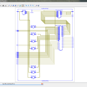
Error Detection and Correction in SRAM Emulated TCAMs
Abstract:
Ternary content addressable memories (TCAMs) are widely used in network devices to implement packet classification. They are used, for example, for packet forwarding, for security, and to implement software-defined networks (SDNs). TCAMs are commonly implemented as standalone devices or as an intellectual property block that is integrated on networking application-specific integrated circuits. On the other hand, field-programmable gate arrays (FPGAs) do not include TCAM blocks. However, the flexibility of FPGAs makes them attractive for SDN implementations, and most FPGA vendors provide development kits for SDN. Those need to support TCAM functionality and, therefore, there is a need to emulate TCAMs using the logic blocks available in the FPGA. In recent years, a number of schemes to emulate TCAMs on FPGAs have been proposed. Some of them take advantage of the large number of memory blocks available inside modern FPGAs to use them to implement TCAMs. A problem when using memories is that they can be affected by soft errors that corrupt the stored bits. The memories can be protected with a parity check to detect errors or with an error correction code to correct them, but this requires additional memory bits per word. In this brief, the protection of the memories used to emulate TCAMs is considered. In particular, it is shown that by exploiting the fact that only a subset of the possible memory contents are valid, most single-bit errors can be corrected when the memories are protected with a parity bit.
List of the following materials will be included with the Downloaded Backup:
Feed forward-Cutset-Free Pipelined Multiply–Accumulate Unit for the Machine Learning Accelerator
Abstract:
Multiply–accumulate (MAC) computations account for a large part of machine learning accelerator operations. The pipelined structure is usually adopted to improve the performance by reducing the length of critical paths. An increase in the number of flip-flops due to pipelining, however, generally results in significant area and power increase. A large number of flip-flops are often required to meet the feed forward-cutset rule. Based on the observation that this rule can be relaxed in machine learning applications, we propose a pipelining method that eliminates some of the flip-flops selectively. The simulation results show that the proposed MAC unit achieved a 20% energy saving and a 20% area reduction compared with the conventional pipelined MAC.
List of the following materials will be included with the Downloaded Backup: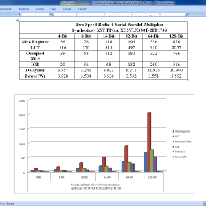
A Two-Speed, Radix-4, Serial–Parallel Multiplier (Booth Multiplier )
Abstract:
In this paper, we present a two-speed, radix-4, serial-parallel multiplier for accelerating applications such as digital filters, artificial neural networks, and other machine learning algorithms. Our multiplier is a variant of the serial–parallel (SP) modified radix-4 Booth multiplier that adds only the nonzero Booth encodings and skips over the zero operations, making the latency dependent on the multiplier value. Two sub circuits with different critical paths are utilized so that throughput and latency are improved for a subset of multiplier values. The multiplier is evaluated on an Intel Cyclone V field-programmable gate array against standard parallel–parallel and SP multipliers across four different process–voltage–temperature corners. We show that for bit widths of 32 and 64, our optimizations can result in a 1.42×–3.36× improvement over the standard parallel Booth multiplier in terms of area–time depending on the input set.
List of the following materials will be included with the Downloaded Backup:
A High-Throughput Hardware Accelerator for Lossless Compression of a DDR4 Command Trace
Abstract:
In a memory system, understanding how the host is stressing the memory is important to improve memory performance. Accordingly, the need for the analysis of memory command trace, which the memory controller sends to the dynamic random access memory, has increased. However, the size of this trace is very large; consequently, a high-throughput hardware (HW) accelerator that can efficiently compress these data in real time is required. This paper proposes a high throughput HW accelerator for lossless compression of the command trace. The proposed HW is designed in a pipeline structure to process Huffman tree generation, encoding, and stream merge. To avoid the HW cost increase owing to high throughput processing, a Huffman tree is efficiently implemented by utilizing static random access memory-based queues and bitmaps. In addition, variable length stream merge is performed at a very low cost by reducing the HW wire width using the mathematical properties of Huffman coding and processing the metadata and the Huffman codeword using FIFO separately. Furthermore, to improve the compression efficiency of the DDR4 memory command, the proposed design includes two preprocessing operations, the “don’t care bits override” and the “bits arrange,” which utilize the operating characteristics of DDR4 memory. The proposed compression architecture with such preprocessing operations achieves a high throughput of 8 GB/s with a compression ratio of 40.13% on average. Moreover, the total HW resource per throughput of the proposed architecture is superior to the previous implementations.
List of the following materials will be included with the Downloaded Backup: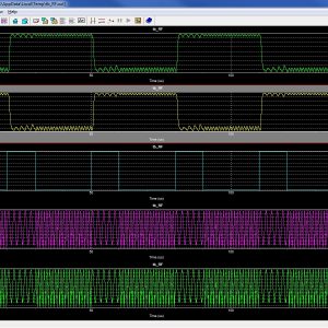
Highly Linear Low-Power Wireless RF Receiver for WSN
Abstract:
This paper introduces a low-power wireless RF receiver for the wireless sensor network. The receiver has improved linearity with incorporated current-mode circuits and high-selectivity filtering. The receiver operates at the 900-MHz industrial, scientific, and medical band and is implemented in 130-nm CMOS technology. The receiver has a frequency multiplication mixer, which uses a 300-MHz clock from a local oscillator (LO). The LO is implemented using vertical delay cells to reduce power consumption. The receiver conversion gain is 40 dB and the receiver noise. The receiver’s input third-order intercept point (IIP3) is −6 dBm and the total power consumption is 1.16 mW.
List of the following materials will be included with the Downloaded Backup: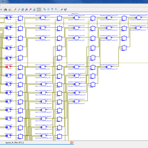
Design of Sparse FIR Filters With Reduced Effective Length
Abstract:
In this paper, an exchange algorithm is proposed to design sparse linear phase finite impulse response (FIR) filters with reduced effective length. The sparse FIR filter design problem is formally an l0-norm minimization problem. This original design problem is re-formulated by encoding the filter coefficients using a binary encoding vector, which represents the locations of the zero and non-zero filter coefficients. An iterative 0-1 exchange process with proper direction control is proposed to propel the minimax approximation error toward the specified upper bound of error for sparsity maximization. The effective length is optimized with a lower priority than sparsity in the proposed algorithm. Simulation results show that the proposed algorithm is superior to the existing algorithms in terms of both sparsity and/or effective length in most cases.
List of the following materials will be included with the Downloaded Backup:
Many-Objective Sizing Optimization of a Class-C/D VCO for Ultralow-Power IoT and Ultralow Phase-Noise Cellular Applications
Abstract:
In this paper, the performance boundaries and corresponding tradeoffs of a complex dual-mode class-C/D voltage controlled oscillator (VCO) are extended using a framework for the automatic sizing of radio frequency integrated circuit blocks, where an all-inclusive test bench formulation enhanced with an additional measurement processing system enables the optimization of “everything at once” toward its true optimal tradeoffs. VCOs embedded in the state-of-the-art multi standard transceivers must comply with extremely high performance and ultralow power requirements for modern cellular and Internet of Things applications. However, the proper analysis of the design tradeoffs is tedious and impractical, as a large amount of conflicting performance figures obtained from multiple modes, test benches, and/or analysis must be considered simultaneously. Here, the dual-mode design and optimization conducted provided 287 design solutions with figures of merit above 192 dBc/Hz, where the power consumption varies from 0.134 to 1.333 mW, the phase noise at 10 MHz from −133.89 to −142.51 dBc/Hz, and the frequency pushing from 2 to 500 MHz/V, on the worst case of the tuning range. These results pushed this circuit design to its performance limits on a 65-nm CMOS technology, reducing 49% of the power consumption of the original design while also showing its potential for ultralow power with more than 93% reduction. In addition, worst case corner criteria were also performed on the top of the worst case tuning range optimization, taking the problem to a human-untrea table LXVI-D performance space.
List of the following materials will be included with the Downloaded Backup:
Energy-Quality Scalable Adders Based on Non-zeroing Bit Truncation
Abstract:
Approximate addition is a technique to trade off energy consumption and output quality in error-tolerant applications. In prior art, bit truncation has been explored as a lever to dynamically trade off energy and quality. In this brief, an innovative bit truncation strategy is proposed to achieve more graceful quality degradation compared to state-of-the-art truncation schemes. This translates into energy reduction at a given quality target. When applied to a ripple-carry adder, the proposed bit truncation approach improves quality by up to 8.5 dB in terms of peak signal-to-noise ratio, compared to traditional bit truncation. As a case study, the proposed approach was applied to a discrete cosine transform engine. In comparison with prior art, the proposed approach reduces energy by 20%, at insignificant delay and silicon area overhead.
List of the following materials will be included with the Downloaded Backup: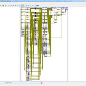
World’s Fastest FFT Architectures: Breaking the Barrier of 100 GS/s
Abstract:
This paper presents the fastest fast Fourier transform (FFT) hardware architectures so far. The architectures are based on a fully parallel implementation of the FFT algorithm. In order to obtain the highest throughput while keeping the resource utilization low, we base our design on making use of advanced shift-and-add techniques to implement the rotators and on selecting the most suitable FFT algorithms for these architectures. Apart from high throughput and resource efficiency, we also guarantee high accuracy in the proposed architectures. For the implementation, we have developed an automatic tool that generates the architectures as a function of the FFT size, input word length and accuracy of the rotations. We provide experimental results covering various FFT sizes, FFT algorithms, and field-programmable gate array boards. These results show that it is possible to break the barrier of 100 GS/s for FFT calculation.
List of the following materials will be included with the Downloaded Backup: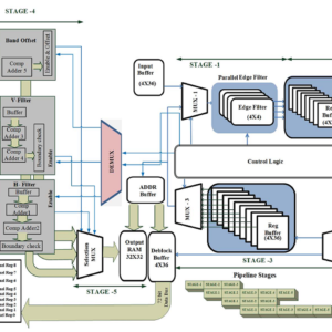
Design and Implementation of Efficient Streaming Deblocking and SAO Filter for HEVC Decoder
We have also Code for 720 x 576 Image Resolution using 64 x 64 Block Size of HEVC. Cost of this Update work in High Resolution Rs. 45,000/- ( Rs. 45,000/- + Rs. 30,000/- ) : Total Cost : Rs. 75,000/-
Abstract:
This paper aims to design an efficient mixed serial five-stage pipeline processing hardware architecture of deblocking filter (DBF) and sample adaptive offset (SAO) filter for high efficiency video coding decoder. The proposed hardware is designed to increase the throughput and reduce the number of clock cycles by processing the pixels in a stream of 4 × 36 samples in which edge filters are applied vertically in a parallel fashion for processing of luma/chroma samples. Subsequently these filtered pixels are transposed and reprocessed through vertical filter for horizontal filtering in a pipeline fashion. Finally, the filtered block transposed back to the original orientation and forwarded to a three-stage pipeline SAO filter. The proposed architecture is implemented in field programmable gate array and application specific integrated circuit platform using 90-nm library. Experimental results illustrate that the proposed DBF and SAO architecture decreases the processing cycles (172) required for processing each 64 × 64 or large coding unit compared with the state-of-the-art literature with the increase of gate count (593.32K) including memory. The results show that the throughput of the proposed filter can successfully decode ultrahigh definition video sequences at 200 frames/s at 341 MHz.
List of the following materials will be included with the Downloaded Backup:
Analysis, Comparison, and Experimental Validation of a Class AB Voltage Follower With Enhanced Bandwidth and Slew Rate
Abstract:
This paper describes a bandwidth (BW)- and slew rate (SR)-enhanced class AB voltage follower (VF). A thorough small signal analysis of the proposed and a state-of-the-art AB-enhanced VF is presented to compare their performance. The proposed circuit has 50-MHz BW, 19.5-V/µs SR, and a BW figure of merit of 41.6 (MHz × pF/µW) for CL = 50 pF. It provides 13 times higher current efficiency and 15 times higher BW than the conventional VF with equal 60-µW static power dissipation. The experimental and simulation results of a fabricated test chip in the 130-nm CMOS technology validate the proposed circuit.
List of the following materials will be included with the Downloaded Backup:
Low-Complexity 2-D Digital FIR Filters Using Polyphase Decomposition and Farrow Structure
Abstract:
This paper proposes a novel realization technique for quadrantally symmetric 2-D finite impulse response filters with a guaranteed reduction in the hardware complexity. Here, the concept of Farrow structure-based interpolation filter design using the polyphase decomposition of the 1-D filter transfer function is effectively utilized in the 2-D domain. The proposed 2-D filter makes use of row-wise polyphase decomposition of the 2-D transfer function or frequency response, followed by the polynomial approximation of the individual polyphase coefficients resulting in Farrow structures corresponding to each row filter. The final coefficients are implemented by varying the delay values in all the Farrow structures, followed by the interpolation of the coefficients obtained from each delay value, which in turn forms the rows in the 2-D kernel. The major highlight of the proposed method is the highly reduced implementation complexity in terms of the number of multipliers and adders, with a low normalized root-mean-square error. Design examples of the circularly symmetric and fan-type filters have been considered to show the efficiency of the approach. The results show a drastic reduction in the implementation complexity of the 2-D filters of upto 20%, with significantly low normalized root-mean-square error lesser than 0.5%.
List of the following materials will be included with the Downloaded Backup:
A Low Complexity I/Q Imbalance Calibration Method for Quadrature Modulator
Abstract:
This brief presents a low-complexity I/Q (in-phase and quadrature components) imbalance calibration method for the transmitter using quadrature modulation. Impairments in analog quadrature modulator have a deleterious effect on the signal fidelity. Among the critical impairments, I/Q imbalance (gain and phase mismatches) deteriorates the residual sideband performance of the analog quadrature modulator degrading the error vector magnitude. Based on the theoretical mismatch analysis of the quadrature modulator, we propose a low-complexity I/Q imbalance extraction algorithm. After the parameter extraction, the transmitter is calibrated by imposing the counter imbalanced mismatch of the transmitter through the digital baseband. In comparison with existing I/Q imbalance calibration methods, the novelty of the proposed method lies in that: 1) only three spectrum measurements of the device-under-test are needed for extraction and calibration of gain and phase mismatches; 2) due to the blind nature of the calibration algorithm, the proposed approach can be readily applicable to an existing I/Q transmitter; 3) no extra hardware that degrades the calibration accuracy is required; and 4) due to the non-iterative nature, the proposed method is faster and computationally more efficient than previously published methods.
List of the following materials will be included with the Downloaded Backup:
Low Power and High Speed Implementation of FIR filter design using CMOS GDI Truncated Multiplier
Abstract:
The logic size, propagation delay, power of applications, based upon this improvement the adder design logic size will reduced year by year, here a proposed In recent technology of any application, adders is a more priority to do a function and task of arithmetic operation, in crucial this adder based arithmetic operation will decide work of this paper will design using a single bit full adder to design a multiplier. In this multiplier design, adder is a main priority to reduce the arithmetic logic size and increases speed of multiplier, in recent we have lots of multiplier design, Vedic multiplier, Wallace tree multiplier, booth multiplier, approximate multiplier. Here, the proposed work will taken truncated multiplier design, it's because, the truncated multiplier will have a capability to reduced internal and external architecture size in every design, regarding this truncated multiplier will have three options such as rounding, deleting, truncating, here the MSB bits will be truncated and present the output of n x n multiplication will provided only n bit level, using this truncated multiplier the proposed work will designed a 8-Tap FIR(Finite impulse response) filter and shown the efficiency of filter design using this CMOS GDI (Gate Diffusion Input) adder design. This proposed work will design in CMOS Logic gate and which 10-T transistor level of full adders with 90um technology, finally proved the terms of area, delay and power.
List of the following materials will be included with the Downloaded Backup:
Improving Error Correction Codes for Multiple-Cell Upsets in Space Applications
Proposed Abstract:
Currently, faults suffered by SRAM memory systems have increased due to the aggressive CMOS integration density. Thus, the probability of occurrence of single-cell upsets (SCUs) or multiple-cell upsets (MCUs) augments. One of the main causes of MCUs in space applications is cosmic radiation. A common solution is the use of error correction codes (ECCs). Nevertheless, when using ECCs in space applications, they must achieve a good balance between error coverage and redundancy, and their encoding/decoding circuits must be efficient in terms of area, power, and delay. Different codes have been proposed to tolerate MCUs. For instance, Matrix codes use Hamming codes and parity checks in a bi-dimensional layout to correct and detect some patterns of MCUs. Recently presented, column–line–code (CLC) has been designed to tolerate MCUs in space applications. CLC is a modified Matrix code, based on extended Hamming codes and parity checks. Nevertheless, a common property of these codes is the high redundancy introduced. In this paper, we present a series of new low redundant ECCs able to correct MCUs with reduced area, power, and delay overheads. Also, these new codes maintain, or even improve, memory error coverage with respect to Matrix and CLC codes.
List of the following materials will be included with the Downloaded Backup:
Approximate Sum-of-Products Design Based on Distributed Arithmetic
Proposed Abstract:
Approximate circuits provide high performance and require low power. Sum-of-products (SOP) units are key elements in many digital signal processing applications. In this brief, three approximate SOP (ASOP) models which are based on the distributed arithmetic are proposed. They are designed for different levels of accuracy. First model of ASOP achieves an improvement up to 64% on area and 70% on power, when compared with conventional unit. Other two models provide an improvement of 32% and 48% on area and 54% and 58% on power, respectively, with a reduced error rate compared with the first model. Third model achieves the mean relative error and normalized error distance as low as 0.05% and 0.009%, respectively. Performance of approximate units is evaluated with a noisy image smoothing application, where the proposed models are capable of achieving higher peak signal to-noise ratio than the existing state-of-the-art techniques. It is shown that the proposed approximate models achieve higher processing accuracy than existing works but with significant improvements in power and performance.
List of the following materials will be included with the Downloaded Backup:
Low-Complexity VLSI Design of Large Integer Multipliers for Fully Homomorphic Encryption
Abstract:
Large integer multiplication has been widely used in fully homomorphic encryption (FHE). Implementing feasible large integer multiplication hardware is thus critical for accelerating the FHE evaluation process. In this paper, a novel and efficient operand reduction scheme is proposed to reduce the area requirement of radix-r butterfly units. We also extend the single port, merged-bank memory structure to the design of number theoretic transform (NTT) and inverse NTT (INTT) for further area minimization. In addition, an efficient memory addressing scheme is developed to support both NTT/INTT and resolving carries computations. Experimental results reveal that significant area reductions can be achieved for the targeted 786 432- and 1 179 648-bit NTT-based multipliers designed using the proposed schemes in comparison with the related works. Moreover, the two multiplications can be accomplished in 0.196 and 2.21 ms, respectively, based on 90-nm CMOS technology. The low-complexity feature of the proposed large integer multiplier designs is thus obtained without sacrificing the time performance.
List of the following materials will be included with the Downloaded Backup:
Input Based Dynamic Reconfiguration of Approximate Arithmetic Units for Video Encoding
Abstract:
The field of approximate computing has receivedsignificant attention from the research community in the pastfew years, especially in the context of various signal processingapplications. Image and video compression algorithms, such asJPEG, MPEG, and so on, are particularly attractive candidatesfor approximate computing, since they are tolerant of computingimprecision due to human imperceptibility, which can beexploited to realize highly power-efficient implementations ofthese algorithms. However, existing approximate architecturestypically fix the level of hardware approximation staticallyand are not adaptive to input data. For example, if afixed approximate hardware configuration is used for anMPEG encoder (i.e., a fixed level of approximation), theoutput quality varies greatly for different input videos. Thispaper addresses this issue by proposing a reconfigurableapproximate architecture for MPEG encoders thatoptimizespower consumption with the goal of maintaining a particularPeak Signal-to-Noise Ratio (PSNR) threshold for any video.We propose two heuristics for automaticallytuning the approximation degree of the RABs in thesetwo modules during runtime based on the characteristics of eachindividual video. The proposed architecture of this paper analysis the logic size, area and power consumption using Xilinx 14.2.
List of the following materials will be included with the Downloaded Backup:
Low Power Split Radix FFT Processors Using Radix 2 Butterfly Units
Split radix fast Fourier Transform (SRFFT) is an ideal candidate for the implementation of a low power FFT processor, because it has the lowest number of arithmetic operation among all the FFT algorithms. In the design of such processors, an efficient addressing scheme for FFT data as well as twiddle factors is required. The signal flow graph of SRFFT is the same as radix-2 FFT, and therefore, the conventional address generation schemes of FFT data could also be applied to SRFFT. However SRFFT has irregular locations of twiddle factors and forbids the application of radix-2 address generation methods. This brief presents a shared memory low power SRFFT processor architecture. The SRFFT can be computed by using a modified radix-2 butterfly unit. The butterfly unit exploits the multiplier-gating technique to save dynamic power at the expense of using more hardware resources. In addition, two novel address generation algorithm for both the trivial and nontrivial twiddle factors are developed. In this paper We increases the architecture size, of radix-4 and 2048 point complex valued transform, and shown the performance of area, power and delay, and synthesized xilinx FPGA on s6lx16-2csg225.
List of the following materials will be included with the Downloaded Backup:
RF Power Gating A Low Power Technique for Adaptive Radios
A Computation and Energy Reduction Technique for HEVC Discrete Cosine Transform
In this paper, a novel computation and energy reduction technique for High Efficiency Video Coding (HEVC) Discrete Cosine Transform (DCT) for all Transform Unit (TU) sizes is proposed. The proposed technique reduces the computational complexity of HEVC DCT significantly at the expense of slight decrease in PSNR and slight increase in bit rate by only calculating several pre-determined low frequency coefficients of TUs and assuming that the remaining coefficients are zero. It reduced the execution time of HEVC HM software encoder up to 12.74%, and it reduced the execution time of DCT operations in HEVC HM software encoder up to 37.27%. In this paper, a low energy HEVC 2D DCT hardware for all TU sizes is also designed and implemented using Verilog HDL. The proposed hardware, in the worst case, can process 53 Ultra HD (7680x4320) video frames per second. The proposed technique reduced the energy consumption of this hardware up to 18.9%. Therefore, it can be used in portable consumer electronics products that require a real-time HEVC encoder. The proposed architecture of this paper analysis the logic size, area and power consumption using Xilinx 14.2.
List of the following materials will be included with the Downloaded Backup:
A New Parallel VLSI Architecture for Real-time Electrical Capacitance Tomography
This paper presents a fixed-point reconfigurable parallel VLSI hardware architecture for real-time Electrical Capacitance Tomography (ECT). Another FPGA module performs the inverse steps of the tomography algorithm. A dual port built-in memory banks store the sensitivity matrix, the actual value of the capacitances, and the actual image with RGB format. A two dimensional (2D) core multiprocessing elements (PE) engine intercommunicates with these memory banks via parallel buses. We are focus only on the FPGA module because the design is decide the power consumption and cost. The proposed architecture of this paper analysis the logic size, area and power consumption using Xilinx 14.2. List of the following materials will be included with the Downloaded Backup:
Provide Wordlwide Online Support
We can provide Online Support Wordlwide, with proper execution, explanation and additionally provide explanation video file for execution and explanations.
24/7 Support Center
NXFEE, will Provide on 24x7 Online Support, You can call or text at +91 9789443203, or email us nxfee.innovation@gmail.com
Terms & Conditions:
Customer are advice to watch the project video file output, and before the payment to test the requirement, correction will be applicable.
After payment, if any correction in the Project is accepted, but requirement changes is applicable with updated charges based upon the requirement.
After payment the student having doubts, correction, software error, hardware errors, coding doubts are accepted.
Online support will not be given more than 3 times.
On first time explanation we can provide completely with video file support, other 2 we can provide doubt clarifications only.
If any Issue on Software license / System Error we can support and rectify that within end of day.
Extra Charges For duplicate bill copy. Bill must be paid in full, No part payment will be accepted.
After payment, to must send the payment receipt to our email id.
Powered by NXFEE INNOVATION, Pondicherry.
Call us today at : +91 9789443203 or Email us at nxfee.innovation@gmail.com
NXFEE Development & Services

Product Categories
- 2014 (12)
- 2015 (39)
- 2016 (31)
- 2017 (16)
- 2018 (17)
- 2019 (42)
- 2020 (29)
- 2021 (16)
- 2022 (22)
- 2023 (17)
- Area Efficient (92)
- High speed VLSI Design (49)
- IEEE (16)
- Image Processing (34)
- Low power VLSI Design (71)
- NOC VLSI Design (3)
- VLSI (180)
- VLSI Application / Interface and Mini Projects (13)
- VLSI_2023 (15)
Filter by price
Product Status
Sort by producents

Copyright © 2021 Nxfee Innovation.