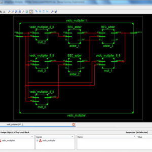
A Comparative Analysis of Multiplier Topologies using Different Vedic Sutras
Abstract: The need of low area and high speed Multiplier is increasing as the need of high speed processors are needed. The multipliers used in Square and cube architecture have to be more efficient in area and also in speed. In this paper a multiplier is implemented based on Nikhilam sutra with binary excess unit. The ripple carry adder in the multiplier architecture increases the speed of addition of partial products. The proposed architecture of this paper analysis the logic size, area and power consumption using Xilinx 14.2.
List of the following materials will be included with the Downloaded Backup:
A Computation and Energy Reduction Technique for HEVC Discrete Cosine Transform
In this paper, a novel computation and energy reduction technique for High Efficiency Video Coding (HEVC) Discrete Cosine Transform (DCT) for all Transform Unit (TU) sizes is proposed. The proposed technique reduces the computational complexity of HEVC DCT significantly at the expense of slight decrease in PSNR and slight increase in bit rate by only calculating several pre-determined low frequency coefficients of TUs and assuming that the remaining coefficients are zero. It reduced the execution time of HEVC HM software encoder up to 12.74%, and it reduced the execution time of DCT operations in HEVC HM software encoder up to 37.27%. In this paper, a low energy HEVC 2D DCT hardware for all TU sizes is also designed and implemented using Verilog HDL. The proposed hardware, in the worst case, can process 53 Ultra HD (7680x4320) video frames per second. The proposed technique reduced the energy consumption of this hardware up to 18.9%. Therefore, it can be used in portable consumer electronics products that require a real-time HEVC encoder. The proposed architecture of this paper analysis the logic size, area and power consumption using Xilinx 14.2.
List of the following materials will be included with the Downloaded Backup:
A Fully Digital Front End Architecture for ECG Acquisition System with 0.5 V Supply
This paper presents a new power-efficient electrocardiogram acquisition system that uses a fully digital architecture to reduce the power consumption and chip area. The proposed architecture is compatible with digital CMOS technology and is capable of operating with a low supply voltage of 0.5 V. In this architecture, no analog block, e.g., low-noise amplifier (LNA), and filters, and no passive elements, such as ac coupling capacitors, are used. A moving average voltage-to time converter is used, which behaves instead of the LNA and anti-aliasing filter. A digital feedback loop is employed to cancel the impact of the dc offset on the circuit, which eliminates the need for coupling capacitors. The proposed architecture of this paper area and power consumption is analysis using tanner tool.
List of the following materials will be included with the Downloaded Backup:
A Fully Static Topologically Compressed 21 Transistor Flip Flop With 75 Percentage of Power Saving
An extremely low-power flip-flop (FF) named topologically-compressed flip-flop (TCFF) is proposed. As compared with conventional FFs, the FF reduces power dissipation by 75% at 0% data activity. This power reduction ratio is the highest among FFs that have been reported so far. The reduction is achieved by applying topological compression method, merger of logically equivalent transistors to an unconventional latch structure. The very small number of transistors, only three, connected to clock signal reduces the power drastically, and the smaller total transistor count assures the same cell area as conventional FFs. In addition, fully static full-swing operation makes the cell tolerant of supply voltage and input slew variation. An experimental chip design with 40 nm CMOS technology shows that almost all conventional FFs are replaceable with proposed FF while preserving the same system performance and layout area. The proposed design is analysis the power and delay by using tanner tools.
List of the following materials will be included with the Downloaded Backup:
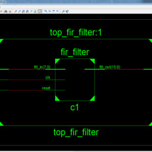
A High Performance FIR Filter Architecture for Fixed and Reconfigurable Applications
Abstract:
Transpose form finite-impulse response (FIR)filters are inherently pipelined and support multiple constant multiplications (MCM) technique that results in significant saving of computation. However, transpose form configuration does not directly support the block processing unlike direct form configuration. In this paper, we explore the possibility of realization of block FIR filter in transpose form configuration for area-delay efficient realization of large order FIR filters for both fixed and reconfigurable applications. Based on a detailed computational analysis of transpose form configuration of FIR filter, we have derived a flow graph for transpose form block FIR filter with optimized register complexity. A generalized block formulation is presented for transpose form FIR filter. We have derived a general multiplier-based architecture for the proposed transpose form block filter for reconfigurable applications. A low-complexity design using the MCM scheme is also presented for the block implementation of fixed FIR filters. The proposed structure involves significantly less area delay product (ADP) and less energy per sample (EPS) than the existing block implementation of direct-form structure for medium or large filter lengths, while for the short-length filters, the block implementation of direct-form FIR structure has less ADP and less EPS than the proposed structure. The proposed architecture of this paper analysis the logic size, area and power consumption using Xilinx 14.2.
List of the following materials will be included with the Downloaded Backup:
A High Speed FPGA Implementation of an RSD Based ECC Processor
In this paper, an exportable application-specific instruction-set elliptic curve cryptography processor based on redundant signed digit representation is proposed. The processor employs extensive pipelining techniques for Karatsuba–Ofman method to achieve high throughput multiplication. Furthermore, an efficient modular adder without comparison and a highthrough put modular divider, which results in a short datapath for maximized frequency, are implemented. The processor supports the recommended NIST curve P256 and is based on an extended NIST reduction scheme. The proposed architecture of this paper analysis the logic size, area and power consumption using Xilinx 14.2.
List of the following materials will be included with the Downloaded Backup:
A Low Cost Low Power All Digital Spread Spectrum Clock Generator
Abstract:
In this brief, a low-cost low-power all-digital spread spectrum clock generator (ADSSCG) is presented. The proposed ADSSCG can provide an accurate programmable spreading ratio with process, voltage, and temperature variations. To maintain the frequency stability while performing triangular modulation, the fast-relocked mechanism is proposed. The proposed fast-relocked ADSSCG is implemented in a standard performance 90-nm CMOS process, and the active area is 200 µm × 200 µm. The experimental results show that the electromagnetic interference reduction is 14.61 dB with a 0.5% spreading ratio and 19.69 dB with a 2% spreading ratio at 270 MHz The power consumption is 443 µW at 270 MHz with a 1.0 V power supply.
List of the following materials will be included with the Downloaded Backup:
A Multiuser Detection Algorithm in the Uplink SCFDMA System for Green Communication network
In mobile network the multiuser detection mostly in 5G networks with using communication of CDMA, SC-FDMA, UTMS, EDGE, FDMA, WI-MAX etc,. Here SC-FDMA (Single Carrier FDMA) plays major role in 5G networks even the performance of improving Low Power Consumption in Low Peak to average ratio of RF Signal Transmission. The iteration of signal transmission in the same manner of Multi User SC-FDMA requires traditional parallel and serial interference cancellation algorithm for achieving the result in large, where the algorithm is consumed to be low power consumption. In the same manner to eliminate the Multiple access RF communication, here the proposed algorithm is introduces in named Optical Weighted Parallel Interference Cancellation (OWPIC). As a result to implement the SC-FDMA with high precision then traditional Parallel Interference Cancellation(PIC) with Multi User SC-FDMA using OWPIC, and also implement this architecture in FPGA (S5LX9) and finally analysis the logic size, low power consumption, high frequency interference, radio signal interference.
List of the following materials will be included with the Downloaded Backup:
A New Parallel VLSI Architecture for Real-time Electrical Capacitance Tomography
This paper presents a fixed-point reconfigurable parallel VLSI hardware architecture for real-time Electrical Capacitance Tomography (ECT). Another FPGA module performs the inverse steps of the tomography algorithm. A dual port built-in memory banks store the sensitivity matrix, the actual value of the capacitances, and the actual image with RGB format. A two dimensional (2D) core multiprocessing elements (PE) engine intercommunicates with these memory banks via parallel buses. We are focus only on the FPGA module because the design is decide the power consumption and cost. The proposed architecture of this paper analysis the logic size, area and power consumption using Xilinx 14.2. List of the following materials will be included with the Downloaded Backup:
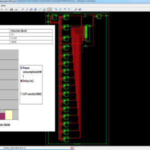
A Novel Quantum Dot Cellular Automata X bit × 32 bit SRAM
Application of quantum-dot cellular automata (QCA) technology as an alternative to CMOS technology on the nanoscale has a promising future; QCA is an interesting technology for building memory. The proposed design and simulation of a new memory cell structure based on QCA with a minimum delay, area, and complexity is presented to implement a static random access memory (SRAM). This paper presents the design and simulation of a 16-bit × 32-bit SRAM with a new structure in QCA. Since QCA is a pipeline, this SRAM has a high operating speed. The 16-bit × 32-bit SRAM has a new structure with a 32-bit width designed and implemented in QCA. It has the ability of a conventional logic SRAM that can provide read/write operations frequently with minimum delay. The 16-bit × 32-bit SRAM is generalized and an n × 16-bit × 32-bit SRAM is implemented in QCA. Novel 16-bit decoders and multiplexers (MUXs) in QCA are presented that have been designed with a minimum number of majority gates and cells. The new SRAM, decoders, and MUXs are designed, implemented, and simulated in QCA using a signal distribution network to avoid the coplanar problem of crossing wires. The QCA-based SRAM cell was compared with the SRAM cell based on CMOS. Results show that the proposed SRAM is more efficient in terms of area, complexity, clock frequency, latency, throughput, and power consumption.
List of the following materials will be included with the Downloaded Backup:
A Thermal Energy Harvesting Power Supply with an Internal Start up Circuit
A complete thermal energy harvesting power supply for implantable pacemakers is presented in this paper. The designed power supply includes an internal startup and does not need any external reference voltage. The startup circuit includes a prestart up charge pump (CP) and a startup boost converter. The prestart up CP consists of an ultralow-voltage oscillator followed by a high-efficiency modified Dickson. Forward body biasing is used to effectively reduce the MOS threshold voltages as well as the supply voltage in oscillator and CP. The steady-state circuit includes a high-efficiency boost converter that utilizes a modified maximum power point tracking scheme. The system is designed so that no failure occurs under overload conditions. Using this approach, a thermal energy harvesting power supply has been designed using 130-nm CMOS technology with low dropout regulator. Finally we are got the output of 2.5V in 10ms.
List of the following materials will be included with the Downloaded Backup:
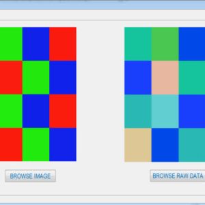
A VLSI Architecture for Watermarking of Gray scale Images using Weighted Median Prediction
Abstract:
Watermarking the digital data is a familiar technique to authenticate and resolve the copyright issues of multimedia data. This paper proposes a new VLSI architecture for watermarking grayscale images using weighted median prediction operation, as this mechanism will have a minimum computation complexity. In this VLSI based data hiding process the secret digital signature is hidden in the host image and analyzed with the PSNR value and Payload capacity.
List of the following materials will be included with the Downloaded Backup:
Algorithm and Architecture for a Low Power Content Addressable Memory Based on Sparse Clustered Networks
Abstract: We propose a low-power content-addressable memory (CAM) employing a new algorithm for associativity between the input tag and the corresponding address of the output data of 128bit. The proposed architecture is based on a recently developed sparse clustered network using binary connections that on-average eliminates most of the parallel comparisons performed during a search. Therefore, the dynamic energy consumption of the proposed design is significantly lower compared with that of a conventional low-power CAM design. Given an input tag, the proposed architecture computes a few possibilities for the location of the matched tag and performs the comparisons on them to locate a single valid match. A design methodology based on the silicon area and power budgets, and performance requirements is discussed. The proposed architecture of this paper will be analysis the logic size, area and power consumption using Xilinx 14.2.
List of the following materials will be included with the Downloaded Backup:
An Efficient Constant Multiplier Architecture Based on Vertical-Horizontal Binary Common Sub-expression Elimination Algorithm for Reconfigurable FIR Filter Synthesis.
Abstract: This paper proposes efficient constant multiplier architecture based on vertical-horizontal binary common sub-expression elimination (VHBCSE) algorithm for designing a reconfigurable finite impulse response (FIR) filter whose coefficients can dynamically change in real time. To design an efficient reconfigurable FIR filter, according to the proposed VHBCSE algorithm, 2-bit binary common sub-expression elimination (BCSE) algorithm has been applied vertically across adjacent coefficients on the 2-D space of the coefficient matrix initially, followed by applying variable-bit BCSE algorithm horizontally within each coefficient. Faithfully rounded truncated multiple constant multiplication/accumulation (MCMAT) and multi-root binary partition graph (MBPG) respectively. Efficiency shown by the results of comparing the FPGA and ASIC implementations of the reconfigurable FIR filter designed using VHBCSE algorithm based constant multiplier establishes the suitability of the proposed algorithm for efficient fixed point reconfigurable FIR filter synthesis.
List of the following materials will be included with the Downloaded Backup:
An Efficient VLSI Architecture of a Reconfigurable Pulse Shaping FIR Interpolation
This brief proposes a two-step optimization technique for designing a reconfigurable VLSI architecture of an interpolation filter for multi-standard digital up converter (DUC) to reduce the power and area consumption. The proposed technique initially reduces the number of multiplications per input sample and additions per input sample by 83% in comparison with individual implementation of each standard’s filter while designing a root-raised-cosine finite-impulse response filter for multi-standard DUC for three different standards. In the next step, a 2-bit binary common sub-expression (BCS)-based BCS elimination algorithm has been proposed to design an efficient constant multiplier, which is the basic element of any filter. This technique has succeeded in reducing the area and power usage by 41% and 38%, respectively, along with 36% improvement in operating frequency over a 3-bit BCS-based technique reported earlier, and can be considered more appropriate for designing the multi-standard DUC. The proposed architecture of this paper analysis the logic size, area and power consumption using Xilinx 14.2.
List of the following materials will be included with the Downloaded Backup:
Area Delay Power Efficient Carry Select Adder
Source : VHDL
Abstract:
We are briefly discussing the logic operations are involved in the CSLA (conventional carry select adder) and the square root conventional carry select adder. We have discard the all the extra logic operations present in the conventional CSLA. In the proposed system carry selection is take place in before the final sum calculation. The proposed system achieves the optimization in the logic units. Finally the FPGA synthesis results shows to achieves a design the low power architecture for CSLA.
List of the following materials will be included with the Downloaded Backup:
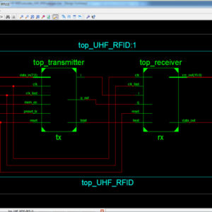
ASIC design of UHF RFID reader digital baseband
This paper presents the ASIC design and implementation of digital baseband system for UHF RFID reader based on EPC Global C1G2 /ISO 18000-6c protocol. The digital baseband system consists of two parts :transmitter and receiver, which including encoding module, decoding module, channel filers, CRC check module, control module and a SPI module. It is described in verilog HDL in RTL level, with Design Complier for synthesizing, PT for static timing analyzing and Astro for physical design. The die is fabricated using IBM 130nm 8-layer-metal RF CMOS process successfully, which size is 3 mm x 3mm, the power consumption is around 6.7mW. It can be applied in the research of single-chip UHF RFID reader. The proposed architecture of this paper analysis the logic size, area and power consumption using Xilinx 14.2.
List of the following materials will be included with the Downloaded Backup:
Block Interleaver Design for High Data Rate Wireless Networks
With increasing data rates in wireless communication, quality of service (QoS) has become a major issue. This is more with fading channels transmitting huge volumes of data. QoS is degraded by inter-symbol interference (ISI) and related errors. One of the simplest and convenient techniques to overcome such errors is interleaving, which is used efficiently in wireless applications. It has found applications for combating burst errors that creeps up in the channel during transmission. In this paper, an efficient model of a block interleaver using a hardware description language (Verilog) is proposed. The proposed technique reduces consumption of FPGA resources to a large extent, which implies low power consumption. The proposed architecture of this paper analysis the logic size, area and power consumption using Xilinx 14.2.
List of the following materials will be included with the Downloaded Backup: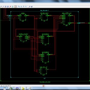
Byte-Reconfigurable LDPC Codec Design With Application to High-Performance ECC of NAND Flash Memory Systems
Abstract: In information theory, a low-density parity-check (LDPC) code is a linear error correcting code, a method of transmitting a message over a noisy transmission channel. An LDPC is constructed using a sparse bipartite graph. LDPC codes are capacity-approaching codes, which means that practical constructions exist that allow the noise threshold to be set very close (or even arbitrarily close on the BEC) to the theoretical maximum (the Shannon limit) for a symmetric memory-less channel. The noise threshold defines an upper bound for the channel noise, up to which the probability of lost information can be made as small as desired. Using iterative belief propagation techniques, LDPC codes can be decoded in time linear to their block length.
List of the following materials will be included with the Downloaded Backup:
Data Encoding Techniques for Reducing Energy Consumption in Network on Chip
Abstract: As the technology shrivel, the power dissipated by the communication subsystem, namely, the routers, NIs, and links. In this paper we are discussed about a set of data encoding and decoding schemes at goal of reduce the power consumption in links of the NoC. This proposed system is transparent and general with respect to the NoC fabric. Finally we are design the area and power efficient encoder and decoder design.
List of the following materials will be included with the Downloaded Backup:
Design and Analysis of Approximate Compressors for Multiplication
Inexact computing is particularly interesting for computer arithmetic designs. Implementation of 8X8 truncated multipliers using Very High Speed Integrated Circuit Hardware Description Language (VHDL). Truncated multipliers can be used in the image multiplication application. This multiplier is automatically truncating the output and reduces the power consumption and are comparing to other multipliers. The proposed architecture of this paper analysis the logic size, area and power consumption using Xilinx 14.2.
List of the following materials will be included with the Downloaded Backup:
Design of 4-bit Ripple carry adder and using 9T full adder
Design of Testable Reversible Sequential Circuits
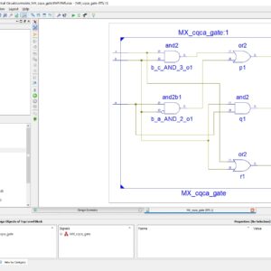
Abstract: In this paper, we propose the design of two vectors testable sequential circuits based on conservative logic gates. The proposed sequential circuits based on conservative logic gates outperform the sequential circuits implemented in classical gates in terms of testability. Any sequential circuit based on conservative logic gates can be tested for classical unidirectional stuck-at faults using only two test vectors. The two test vectors are all 1s, and all 0s. The designs of two vectors testable latches, master-slave flip-flops and double edge triggered (DET) flip-flops are presented. The importance of the proposed work lies in the fact that it provides the design of reversible sequential circuits completely testable for any stuck-at fault by only two test vectors, thereby eliminating the need for any type of scan-path access to internal memory cells. The reversible design of the DET flip-flop is proposed for the first time in the literature. We also showed the application of the proposed approach toward 100% fault coverage for single missing/additional cell defect in the quantum dot cellular automata (QCA) layout of the Fredkin gate. We are also presenting a new conservative logic gate called multiplexer conservative QCA gate (MX-cqca) that is not reversible in nature but has similar properties as the Fredkin gate of working as 2:1 multiplexer. The proposed MX-cqca gate surpasses the Fredkin gate in terms of complexity (the number of majority voters), speed, and area.
List of the following materials will be included with the Downloaded Backup:
Dual Use of Power Lines for Design for Testability A CMOS Receiver Design
As the circuit complexity increases, the number of internal nodes increases proportionally, and individual internal nodes are less accessible due to the limited number of available I/O pins. To address the problem, we proposed power line communications (PLCs) at the IC level, specifically the dual use of power pins and power distribution networks for application/ observation of test data as well as delivery of power. A PLC receiver presented in this paper intends to demonstrate the proof of concept, specifically the transmission of data through power lines. The main design objective of the proposed PLC receiver is the robust operation under variations and droops of the supply voltage rather than high data speed. The PLC receiver is designed and fabricated in CMOS 0.18-µm technology under a supply voltage of 1.8V.
List of the following materials will be included with the Downloaded Backup:
FPGA Implementation of Partially Parallel Encoder Architecture for Long Polar Code
Polar coding is an encoding/decoding scheme that provably achieves the capacity of the class of symmetric binary memory-less channels. Due to the channel achieving property, the polar code has become one of the most favourable error-correcting codes. As the polar code achieves the property asymptotically, however, it should be long enough to have a good error-correcting performance. Although previous fully parallel encoder is intuitive and easy to implement, it is not suitable for long polar codes because of the huge hardware complexity required. In the brief, we analyse the encoding process in the viewpoint of very large-scale integration implementation and propose a new efficient encoder architecture that is adequate for long polar codes and effect in alleviating the hardware complexity. As the proposed encoder allows high-throughput encoding with small hardware complexity, it can be systematically applied to the design of any polar code and to any level of parallelism. Finally shown the power, area, delay report with comparison of existing work.
List of the following materials will be included with the Downloaded Backup:
Full Swing Local Bitline SRAM Architecture Based on the 22 nm FinFET Technology for Low Voltage Operation
The previously proposed average-8T static random access memory (SRAM) has a competitive area and does not require a write-back scheme. In the case of an average-8T SRAM architecture, a full-swing local bitline (BL) that is connected to the gate of the read buffer can be achieved with a boosted wordline (WL) voltage. However, in the case of an average-8T SRAM based on an advanced technology, such as a 22-nm FinFET technology, where the variation in threshold voltage is large, the boosted WL voltage cannot be used, because it degrades the read stability of the SRAM. Thus, a full-swing local BL cannot be achieved, and the gate of the read buffer cannot be driven by the full supply voltage (VDD), resulting in a considerably large read delay. To overcome the above disadvantage, in this paper, a differential SRAM architecture with a full-swing local BL is proposed. In the proposed SRAM architecture, full swing of the local BL is ensured by the use of cross-coupled pMOSs, and the gate of the read buffer is driven by a full VDD, without the need for the boosted WL voltage. Various configurations of the proposed SRAM architecture, which stores multiple bits, are analyzed in terms of the minimum operating voltage and area per bit. The proposed SRAM that stores four bits in one block can achieve a minimum voltage of 0.42 V and a read delay that is 62.6 times lesser than that of the average-8T SRAM based on the 22-nm FinFET technology. The proposed architecture of this paper is analysis the area and power consumption using tanner tool.
List of the following materials will be included with the Downloaded Backup:

Fully Pipelined Low-Cost and High-Quality Color Demosaicking VLSI Design for Real-Time Video Applications
This system presents a fully pipelined color demosaicking design. To improve the quality of reconstructed images, a linear deviation compensation scheme was created to increase the correlation between the interpolated and neighboring pixels. Furthermore, immediately interpolated green color pixels are first to be used in hardware-oriented color demosaicking algorithms, which efficiently promoted the quality of the reconstructed image. A boundary detector and boundary mirror machine were added to improve the quality of pixels located in boundaries. In addition, a hardware sharing technique was used to reduce the hardware costs of three interpolators. Finally these are implemented and get the simulated result is compared to the previous architecture. The code are simulated and power, area, cost are taken using Xilinx 14.2 software and MATLAB. Compared with the previous low complexity designs, this work has the benefits in terms of low cost, low power consumption, and high performance.
List of the following materials will be included with the Downloaded Backup:
Fully Reused VLSI Architecture of FM0Manchester Encoding Using SOLS Technique for DSRC Applications
The dedicated short-range communication (DSRC) is an emerging technique to push the intelligent transportation system into our daily life. The DSRC standards generally adopt FM0 and Manchester codes to reach dc-balance, enhancing the signal reliability. Nevertheless, the coding-diversity between the FM0 and Manchester codes seriously limits the potential to design a fully reused VLSI architecture for both. In this paper, the similarity-oriented logic simplification (SOLS) technique is proposed to overcome this limitation. The encoding capability of this paper can fully support the DSRC standards of America, Europe, and Japan. This paper not only develops a fully reused VLSI architecture, but also exhibits an efficient performance compared with the existing works. The proposed architecture of this paper analysis the logic size, area and power consumption using Xilinx 14.2.
List of the following materials will be included with the Downloaded Backup:
High Speed Low Power and Highly Reliable Frequency Multiplier for DLL Based Clock Generator
To propose a novel frequency multiplier with high-speed, low-power, and highly reliable design for a delay-locked loop-based clock generator to generate a multiplied clock with a high frequency and wide frequency range. The proposed edge combiner achieves a high-speed and highly reliable operation using a hierarchical structure and an overlap canceller. In addition, by applying the logical effort to the pulse generator and multiplication-ratio control logic design, the proposed frequency multiplier minimizes the delay difference between positive- and negative-edge generation paths, which causes a deterministic jitter. Finally, a numerical analysis is performed to analyze and compare the performance of the proposed frequency multiplier with that of previous frequency multipliers. The proposed frequency multiplier is fabricated using a 0.13-µm CMOS process technology, and has the multiplication ratios of 1, 2, 4, 8, and 16, and an output range of 50 MHz–3.3 GHz. The frequency multiplier achieves power consumption is 17.49mW. The proposed architecture of this paper is analysis the logic size, area and power consumption using tanner tool.
List of the following materials will be included with the Downloaded Backup:
Implementation of Subthreshold Adiabatic Logic for Ultralow Power Application
Abstract:
The Subthreshold adiabatic logic for Ultralow power application is a novel approach is efficient in low speed operations, where power consumption and longevity are the pivotal concerns instead of performance. Here, we are implementing the adiabatic logic gates and implementing CLA 8-bit, it will compared to the normal logic gates, the adiabatic logic makes a more power consumption and also increasing speed. The schematic and layout of a 4-bit carry look ahead adder (CLA) has been implemented to show the workability of the proposed logic. The effect of temperature and process parameter variations on sub threshold adiabatic logic-based 4-bit CLA has also been addressed separately. Post layout simulations show that sub threshold adiabatic units can save significant energy compared with a logically equivalent static CMOS implementation.
List of the following materials will be included with the Downloaded Backup:
JF-Cut: A Parallel Graph Cut Approach for Large-Scale Image and Video
Graph cut has proven to be an effective scheme to solve a wide variety of segmentation problems in vision and graphics community. The main limitation of conventional graph-cut implementations is that they can hardly handle large images or videos because of high computational complexity. Even though there are some parallelization solutions, they commonly suffer from the problems of low parallelism (on CPU) or low convergence speed (on GPU). In this paper, we present a novel graph-cut algorithm that leverages a parallelized jump flooding technique and an heuristic push-relabel scheme to enhance the graph-cut process, namely, back-and-forth relabel, convergence detection, and block-wise push-relabel. The entire process is parallelizable on GPU, and outperforms the existing GPU-based implementations in terms of global convergence, information propagation, and performance. We design an intuitive user interface for specifying interested regions in cases of occlusions when handling video sequences. Experiments on a variety of data sets, including images (up to 15 K×10 K), videos (up to 2.5K×1.5K×50), and volumetric data, achieve highquality results and a maximum 40-fold (139-fold) speedup over conventional GPU (CPU-)-based approaches.
List of the following materials will be included with the Downloaded Backup: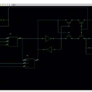
Level-Converting Retention Flip-Flop for Reducing Standby Power in ZigBee SoCs
Abstract: In this paper, we are proposed a level converting retention flip-flop for Zigbee Soc, it will be using to allows the voltage regulator that generates the core supply voltage (VDD, core), to be turned off in the standby mode, and it thus reduces the standby power of the Zigbee Soc. Here the Level up conversion form VDD core is achieved by and embedded nMOS pass transistor level-conversion scheme that uses a low only signal transmitting technique. By embedding a retention latch and level-up converter into the data-to-output path of the proposed RFF, the RFF resolves the problems of the static RAM-based RFF, such as large dc current and low readability caused by threshold drop. The proposed RFF does not also require additional control signals for power mode transitioning. Using 0.13-μm process technology, we implemented an RFF with VDD,core and VDD,IO of 1.2 and 2.5 V, respectively. The maximum operating frequency is 300 MHz. The active energy of the RFF is 191.70 fJ, and its standby power is 350.25 pW.
List of the following materials will be included with the Downloaded Backup: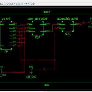
Low Power Compressor Based MAC Architecture for DSP Applications
This paper presents the low power compressor based Multiply-Accumulate (MAC) architecture for DSP applications. In VLSI, highly computed arithmetic cells including adders and multipliers are the most copiously used components. Efficient implementation of arithmetic logic units, floating point units and other dedicated functional components are utilized in most of the microprocessors and digital signal processors (DSPs). Thus in this brief, compressor circuit has been illustrated for the low power applications and also the impact of datapath circuits has been demonstrated. The proposed low power compressor architecture was applied to MAC unit and compared against the conventional compressor based MAC units and observed that the proposed architecture has reduced significant amount of leakage power. The proposed architecture of this paper analysis the logic size, area and power consumption using Xilinx 14.2.
List of the following materials will be included with the Downloaded Backup:
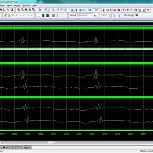
Low Power ECG Based Processor for Predicting Ventricular Arrhythmia
This paper presents the design of a fully integrated electrocardiogram (ECG) signal processor (ESP) for the prediction of ventricular arrhythmia using a unique set of ECG features and a naive Bayes classifier. Real-time and adaptive techniques for the detection and the delineation of the P-QRS-T waves were investigated to extract the fiducial points. We are also detecting the all interval in the ECG signal and compare the stored record for Ventricular Arrhythmia with also energy/area architecture design. The proposed architecture of this paper analysis the logic size, area and power consumption using Xilinx 14.2.
List of the following materials will be included with the Downloaded Backup:
Low-Cost High-Performance VLSI Architecture for Montgomery Modular Multiplication
Source Code : VHDL & VERILOG HDL
Abstract: This paper proposes a simple and efficient Montgomery multiplication algorithm such that the low-costand high-performance Montgomery modular multiplier can be implemented accordingly. The proposed multiplier output data with representation and uses only one parallel prefix adder to avoid a carry propagation and reduce the area, power and delay, and also increasing the speed. Mainly the usage of parallel prefix adder is to reduce the significant delay reduction and area × time2 improvements, all this at the cost of higher power consumption, which is the main reason preventing the use of parallel-prefix adders to achieve high-speed reverse converters in nowadays systems. Hence, to solve the high power consumption problem, novel specific hybrid parallel-prefix-based adder components those provide better trade-off between delay and power consumption. As a result, the extra clock cycles for operand pre-computation and format conversion can be hidden and high throughput can be obtained. Experimental results show that the proposed Montgomery modular multiplier can achieve higher performance and significant area–time product improvement when compared with previous designs. Using VHDL to design the RTL, and the result to be shown in Xilinx 14.2 with Power consumption and area reduction.
List of the following materials will be included with the Downloaded Backup:
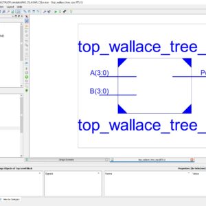
Modified Wallace Tree Multiplier using Efficient Square Root Carry Select Adder
A multiplier is one of the key hardware blocks in most digital and high performance systems such as FIR filters, micro processors and digital signal processors etc. A system’s performance is generally determined by the performance of the multiplier because the multiplier is generally the slowest element in the whole system and also it is occupying more area consuming. The Carry Select Adder (CSLA) provides a good compromise between cost and performance in carry propagation adder design. A Square Root Carry Select Adder using RCA is introduced but it offers some speed penalty. However, conventional CSLA is still area-consuming due to the dual ripple carry adder structure. In the proposed work, generally in Wallace multiplier the partial products are reduced as soon as possible and the final carry propagation path carry select adder is used. In this paper, modification is done at gate level to reduce area and power consumption. The Modified Square Root Carry Select-Adder (MCSLA) is designed using Common Boolean Logic and then compared with regular CSLA respective architectures, and this MCSLA is implemented in Wallace Tree Multiplier. This work gives the reduced area compared to normal Wallace tree multiplier. Finally an area efficient Wallace tree multiplier is designed using common Boolean logic based square root carry select adder.
List of the following materials will be included with the Downloaded Backup:
Obfuscating DSP Circuits via High Level Transformations
This paper presents a novel approach to design obfuscated circuits for digital signal processing (DSP) applications using high-level transformations, a key-based obfuscating finite-state machine (FSM), and a reconfigurator. The goal is to design DSP circuits that are harder to reverse engineer. High level transformations of iterative data-flow graphs have been exploited for area-speed-power tradeoffs. This is the first attempt to develop a design flow to apply high level transformations that not only meet these tradeoffs but also simultaneously obfuscate the architectures both structurally and functionally. Functional obfuscation is accomplished by requiring use of the correct initialization key, and configure data. Structural obfuscation is also achieved by the proposed methodology via high-level transformations. The proposed architecture of this paper analysis the logic size, area and power consumption using Xilinx 14.2
List of the following materials will be included with the Downloaded Backup:
Pre Encoded Multipliers Based on Non Redundant Radix 4 Signed Digit Encoding
Abstract: In this paper we are discussed about the new design of pre-encoded multiplier are explored at offline the standard co efficient and storing them in system memory. The co efficient is used in non redundant radix 4 signed digit form. This encoding technique is less complex partial product implementation and more area and power efficient design. Analysis is verifies the proposed system is efficient from the existing system.
List of the following materials will be included with the Downloaded Backup:
Quaternary Logic Lookup Table in Standard CMOS
Abstract: Interconnections are increasingly the dominant contributor to delay, area and energy consumption in CMOS digital circuits. The proposed implementation overcomes several limitations found in previous quaternary implementations published so far, such as the need for special features in the CMOS process or power-hungry current-mode cells. We have to use the 512bit quaternary Look Up Table for high level of operations in the FPGA. The proposed architecture of this paper will be planned to implemented and also analysis the output current, output voltage, area using Xilinx 14.3.
List of the following materials will be included with the Downloaded Backup:
Quaternary Logic Lookup Table in Standard CMOS
Abstract: Interconnections are increasingly the dominant contributor to delay, area and energy consumption in CMOS digital circuits. The proposed implementation overcomes several limitations found in previous quaternary implementations published so far, such as the need for special features in the CMOS process or power-hungry current-mode cells. We have to use the 512bit quaternary Look Up Table for high level of operations in the FPGA.The proposed architecture of this paper will be planned to implemented and also analysis the output current, output voltage, area using Xilinx 14.3.
List of the following materials will be included with the Downloaded Backup:
Recursive Approach to the Design of a Parallel Self Timed Adder
Abstract: We are briefly discussed about the 64bit parallel self timed adder based on the recursive formulation. The adder is also based on the asynchronous logic circuit and the transistor is connected in parallel. This adder is chance the path automatically, so the delay is configures automatically. The completion detection unit is given the additional support for practical implementation. The simulation is take place with 130nm CMOS technology for the adder circuit. Finally the power consumption for 64bit adder is 0.29mW.
List of the following materials will be included with the Downloaded Backup:
Reverse Converter Design via Parallel-Prefix Adders: Novel Components, Methodology, and Implementations
Abstract: The implementation of residue number system reverse converters based on well-known regular and modular parallel prefix adders is analyzed. The VLSI implementation results show a significant delay reduction and area × time2 improvements, all this at the cost of higher power consumption, which is the main reason preventing the use of parallel-prefix adders to achieve high-speed reverse converters in nowadays systems. Hence, to solve the high power consumption problem, novel specific hybrid parallel-prefix-based adder components those provide better tradeoff between delay and power consumption. The power, area and delay of the proposed system are analysis using Xilinx 14.2.
List of the following materials will be included with the Downloaded Backup: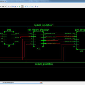
Seizure Prediction using Hilbert Huang Transform on Field Programmable Gate Array
The Hilbert Huang Transform (HHT) has been used extensively in the time-frequency analysis of electroencephalography (EEG) signals and Brain-Computer Interfaces. Most studies utilizing the HHT for extracting features in seizure prediction have used intracranial EEG recordings. Invasive implants in the cortex have unknown long term consequences and pose the risk of complications during surgery. This added risk dimension makes them unsuitable for continuous monitoring as would be the requirement in a Body Area Network. We present an HHT based system on Field Programmable Gate Array (FPGA) for predicting epileptic seizures using scalp EEG. We use bandwidth features of Intrinsic Mode Functions and obtain a classification accuracy of close to 100% using patient-specific classifiers in software. Details of FPGA implementation are also given. The proposed architecture of this paper analysis the logic size, area and power consumption using Xilinx 14.2.
List of the following materials will be included with the Downloaded Backup:
Sharing Logic for Built In Generation of Functional Broadside Tests
Abstract: We are discussed about the built in generation for logic blocks. The advantage of this technique is identifying the similar characteristics of the each logical block. Functional broadside tests are important for addressing overtesting of delay faults as well as avoiding excessive power dissipation during test application. Finally to analysis the performance of the built in generation technique and compare to existing system.
List of the following materials will be included with the Downloaded Backup: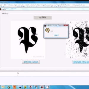
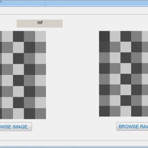
VLSI Implementation of Efficient Image Watermarking Algorithm
Abstract:
The watermarking is the important multimedia content for authentication and security in nowadays. We are proposed to implement the watermarking in FPGA with VLSI architecture. And also use the Haar discrete wallet transform and bit plane slicing for creating the water marking images and extracted watermark images. The area, power, delay of the proposed architecture is analysis using Xilinx 14.2.
List of the following materials will be included with the Downloaded Backup: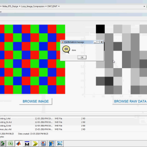
VLSI-Oriented Lossy Image Compression Approach using DA-Based 2D-Discrete Wavelet
We introduced a Discrete Wavelet Transform (DWT) based VLSI-oriented lossy image compression approach, widely used as the core of digital image compression. Here, Distributed Arithmetic (DA) technique is applied to determine the wavelet coefficients, so that the number of arithmetic operation can be reduced substantially. As well, the compression rate is enhanced with the aid of introducing RW block that blocks some of the coefficients obtained from the high pass filter to zero. Subsequently, Differential Pulse-Code Modulation (DPCM) and huffman-encoding are applied to acquire the binary sequence of the image. The proposed architecture of this paper analysis the logic size, area and power consumption using Xilinx 14.2.
List of the following materials will be included with the Downloaded Backup:Provide Wordlwide Online Support
We can provide Online Support Wordlwide, with proper execution, explanation and additionally provide explanation video file for execution and explanations.
24/7 Support Center
NXFEE, will Provide on 24x7 Online Support, You can call or text at +91 9789443203, or email us nxfee.innovation@gmail.com
Terms & Conditions:
Customer are advice to watch the project video file output, and before the payment to test the requirement, correction will be applicable.
After payment, if any correction in the Project is accepted, but requirement changes is applicable with updated charges based upon the requirement.
After payment the student having doubts, correction, software error, hardware errors, coding doubts are accepted.
Online support will not be given more than 3 times.
On first time explanation we can provide completely with video file support, other 2 we can provide doubt clarifications only.
If any Issue on Software license / System Error we can support and rectify that within end of day.
Extra Charges For duplicate bill copy. Bill must be paid in full, No part payment will be accepted.
After payment, to must send the payment receipt to our email id.
Powered by NXFEE INNOVATION, Pondicherry.
Call us today at : +91 9789443203 or Email us at nxfee.innovation@gmail.com
NXFEE Development & Services

Copyright © 2021 Nxfee Innovation.