78 Products found
An Innovative Area Efficient Pixel Shuffling Method for Image Encryption Algorithm
Proposed Abstract:
In image processing and computer vision, pixel shuffling is a method used to increase an image's resolution without adding more parameters or network complexity. With this technique, a low-quality image's pixels are rearranged to produce an output with a better resolution. Pixel shuffling has proven successful in a number of applications, such as image synthesis, super-resolution, and style transfer. Its simplicity and efficiency make it an attractive option for tasks where increasing image resolution is essential, while avoiding the computational overhead associated with more complex architectures. The image line buffer based pixel shuffling technique presented in this study is an alternative to the classic method, which takes up more logic space in VLSI implementations. This proposed method splits and reconstructs the source photos using a 5x5 image line buffer. With the use of block interleave techniques, this pixel shuffling approach handled row and column sequence using this 5x5 picture line buffer. In conclusion, this study was compared with the PSNR and SSIM value; comparisons of logic sizes for area, latency, and power were also examined.
List of the following materials will be included with the Downloaded Backup:
FPGA Implementation of Image Line Buffer to Split and reconstruct a 3×3 size of image pixel with using FIFO Design
Proposed Abstract:
Image line buffers are used in several kinds of image processing applications, particularly where operations must be executed on a per-line basis in order to optimize efficiency. There are many typical applications associated with this technology, including real-time video processing, image filtering, edge detection, computer vision, memory optimization, parallel processing, compression algorithms, and medical imaging. In the context of image and video processing applications, the use of image line buffers may contribute to the optimization of operations when dealing with a continuous stream of frames processed in real time. In the context of image processing, convolutional processes are often used for tasks like as image filtering and blurring. These operations are typically carried out on a per-pixel basis, wherein the value assigned to each pixel is determined by the values of its adjacent pixels. The proposed structure was created using a First-In-First-Out (FIFO) based approach, aiming to decrease the number of logic sizes and complexity in Very Large Scale Integration (VLSI) design architecture. The conversion of design images to hexadecimal and hexadecimal to image format is accomplished using MATLAB GUI applications. These applications also facilitate the comparison of Peak Signal-to-Noise Ratio (PSNR) and Structural Similarity Index Measure (SSIM) values. The internal architecture of the system is implemented using Verilog Hardware Description Language (HDL). Additionally, the simulation is conducted using Modelsim. Furthermore, the system's performance parameters, including area, delay, and power consumption, are compared with those of the Xilinx Vertex-5 Field Programmable Gate Array (FPGA).
List of the following materials will be included with the Downloaded Backup:
FPGA Heart Rate Monitoring (Pre Processing – QRS Detection Stage)
Base Paper Abstract:
The continuous monitoring of cardiac patients requires an ambulatory system that can automatically detect heart diseases. This study presents a new field programmable gate array (FPGA)-based hardware implementation of the QRS complex detection. The proposed detection system is mainly based on the Pan and Tompkins algorithm, but applying a new, simple, and efficient technique in the detection stage. The new method is based on the centered derivative and the intermediate value theorem, to locate the QRS peaks. The proposed architecture has been implemented on FPGA using the Xilinx System Generator for digital signal processor and the Nexys-4 FPGA evaluation kit. To evaluate the effectiveness of the proposed system, a comparative study has been performed between the resulting performances and those obtained with existing QRS detection systems, in terms of reliability, execution time, and FPGA resources estimation. The proposed architecture has been validated using the 48 half-hours of records obtained from the Massachusetts Institute of Technology - Beth Israel Hospital (MITBIH) arrhythmia database. It has also been validated in real time via the analogue discovery device.
List of the following materials will be included with the Downloaded Backup:
Approximate Pruned and Truncated Haar Discrete Wavelet Transform VLSI Hardware for Energy-Efficient ECG Signal Processing
Abstract:
The approximate computing paradigm emerged as a key alternative for trading off accuracy and energy efficiency. Error-tolerant applications, such as multimedia and signal processing, can process the information with lower-than-standard accuracy at the circuit level while still fulfilling a good and acceptable service quality at the application level. The automatic detection of R-peaks in an electrocardiogram (ECG) signal is the essential step preceding ECG processing and analysis. The Haar discrete wavelet transform (HDWT) is a low-complexity pre-processing filter suitable to detect ECG R-peaks in embedded systems like wearable devices, which are incredibly energy constrained. This work presents an approximate HDWT hardware architecture for ECG processing at very high energy efficiency. Our best-proposal employing pruning within the approximate HDWT hardware architecture requires just seven additions. The use of a truncation technique to improve energy efficiency is also investigated herein by observing the evolution of the signal-to-noise ratio and the ultimate impact in the ECG peak-detection application. This research finds that our HDWT approximate hardware architecture proposal accepts higher truncation levels than the original HDWT. In summary: Our results show about 9 times energy reduction when combining our HDWT matrix approximation proposal with the pruning and the highest acceptable level of truncation while still maintaining the R-peak detection performance accuracy of 99.68% on average.
List of the following materials will be included with the Downloaded Backup:
A Configurable Floating Point Multiple Precision Processing Element for HPC and AI Converged Computing
Abstract:
There is an emerging need to design configurable accelerators for the high-performance computing (HPC) and artificial intelligence (AI) applications in different precisions. Thus, the floating-point (FP) processing element (PE), which is the key basic unit of the accelerators, is necessary to meet multiple-precision requirements with energy-efficient operations. However, the existing structures by using high-precision-split (HPS) and low-precision-combination (LPC) methods result in low utilization rate of the multiplication array and long multi term processing period, respectively. In this article, a configurable FP multiple-precision PE design is proposed with the LPC structure. Half precision, single precision, and double precision are supported. The 100% multiplier utilization rate of the multiplication array for all precisions is achieved with improved speed in the comparison and summation process. The proposed design is realized in a 28-nm process with 1.429-GHz clock frequency. Compared with the existing multiple-precision FP methods, the proposed structure achieves 63% and 88% areasaving performance for FP16 and FP32 operations, respectively. The 4× and 20× maximum throughput rates are obtained when compared with fixed FP32 and FP64 operations. Compared with the previous multiple-precision PEs, the proposed one achieves the best energy-efficiency performance with 975.13 GFLOPS/W.
List of the following materials will be included with the Downloaded Backup: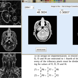
FPGA implementation of low power and high speed image edge detection algorithm
Abstract:
Image processing is a vital task in data processing system for applications in medical fields, remote sensing, microscopic imaging etc., Algorithms for processing image exist except for real time system style, hardware implementation is most popular principally. This paper presents a design for Sobel filter based edge detection on Field Programmable Gate Array (FPGA) board. Hardware implementation of the Sobel edge detection algorithm is chosen because it presents an honest scope for similarity over software package. On the opposite hand, Sobel edge detection will work with less deterioration in high level of noise. Edges are primarily the noticeable variation of intensities in a picture. Edges facilitate to spot the placement of an object and also the boundary of a selected entity within the image. It conjointly helps in feature extraction and pattern recognition. Hence, edge detection is of nice importance in pc vision. The planned design for edge detection exploitation Sobel algorithm is designed using structural Verilog lipoprotein synthesized exploitation Cadence Genus and enforced using Cadence Innovus. The practicality of the planning is verified exploitation normal pictures by FPGA implementation. The proposed architecture reduce the power, delay and space complexity compare to three existing architectures.
List of the following materials will be included with the Downloaded Backup:
Vital-Sign Processing Receiver With Clutter Elimination Using Servo Feedback Loop for UWB Pulse Radar System
Abstract:
This brief presents a vital-sign processing circuit for simultaneous dc/near-dc elimination and out-of-band interference rejection without any digital signal processing or algorithm assistance for the ultra wideband (UWB) pulse-based radar system. An intrinsic self balanced MOS diode (SBMD) was proposed as a stable and balanced pseudo resistor applied under a servo feedback loop in a vital-sign receiver of the sensing radar to perform as a high-pass filter (HPF) with an ultralow corner frequency lower than 0.5 Hz for removing undesired clutters of the reflected signals and input dc-offset voltages from innate circuit offsets. A third-order switched-capacitor (SC) Chebyshev low-pass filter (LPF) with leap-frog topology as the subsequent stage was adopted to suppress the out-band noises, thereby establishing an integrated vital-sign processing circuit with band pass frequency response and incorporating it into a radar module to verify its viability.
List of the following materials will be included with the Downloaded Backup: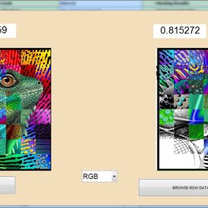
VLSI Implementation of an Edge-Oriented Image Scaling Processor
Abstract:
Image scaling is a very important technique and has been widely used in many image processing applications. In this paper, we present an edge-oriented area-pixel scaling processor. To achieve the goal of low cost, the area-pixel scaling technique is implemented with a low-complexity VLSI architecture in our design. A simple edge catching technique is adopted to preserve the image edge features effectively so as to achieve better image quality. Compared with the previous low-complexity techniques, our method performs better in terms of both quantitative evaluation and visual quality. The seven-stage VLSI architecture of our image scaling processor contains 10.4-K gate counts and yields a processing rate of about 200 MHz by using TSMC 0.18- m technology.
List of the following materials will be included with the Downloaded Backup: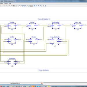
RoBA Multiplier A Rounding Based Approximate Multiplier for High Speed yet Energy Efficient Digital Signal Processing
Abstract:
In this paper, we propose an approximate multiplier that is high speed yet energy efficient. The approach is to round the operands to the nearest exponent of two. This way the computational intensive part of the multiplication is omitted improving speed and energy consumption at the price of a small error. The proposed approach is applicable to both signed and unsigned multiplications. We propose three hardware implementations of the approximate multiplier that includes one for the unsigned and two for the signed operations. The efficiency of the proposed multiplier is evaluated by comparing its performance with those of some approximate and accurate multipliers using different design parameters. In addition, the efficacy of the proposed approximate multiplier is studied in two image processing applications, i.e., image sharpening and smoothing.
List of the following materials will be included with the Downloaded Backup:
VLSI Implementation of Efficient Image Watermarking Algorithm
Abstract:
The watermarking is the important multimedia content for authentication and security in nowadays. We are proposed to implement the watermarking in FPGA with VLSI architecture. And also use the Haar discrete wallet transform and bit plane slicing for creating the water marking images and extracted watermark images. The area, power, delay of the proposed architecture is analysis using Xilinx 14.2.
List of the following materials will be included with the Downloaded Backup:
FPGA Implementation of High Performance Reversible logic based 16×16 Array Multiplier
Proposed Abstract:
In this recent technology of digital gadgets and digital signal processing and image processing method will have more priority in arithmetic operation, such as multiplication, divisions, addition and subtractions. In this operations of arithmetic unit will have number of garbage signal with more memory logic element, due to this problem these arithmetic operations will take more area, delay and power in VLSI system design. Here, this proposed work will present a arithmetic operation using reversible logic method, thus it take memory less logic and less garbage elements, therefore here this reversible logic method will integrated using reversible half adders and full adder in array multiplier and proved the performance with less garbage signals. Finally, this work will have integrated in Verilog HDL, simulated in Modelsim and Synthesized in Xilinx FPGA, and also compared all the parameter in terms of area, delay and power.
List of the following materials will be included with the Downloaded Backup:
An Ultra-Efficient Approximate Multiplier with Error Compensation for Error-Resilient Applications
Base Paper Abstract:
Approximate computing is a promising paradigm for trading off accuracy to improve hardware efficiency in error-resilient applications such as neural networks and image processing. This brief presents an ultra-efficient approximate multiplier with error compensation capability. The proposed multiplier considers the least significant half of the product a constant compensation term. The other half is calculated precisely to provide an ultra-efficient hardware-accuracy tradeoff. Furthermore, a low-complexity but effective error compensation module (ECM) is presented, significantly improving accuracy. The proposed multiplier is simulated using HSPICE with 7nm tri-gate Fin FET technology. The proposed design significantly improves the energy-delay product, on average, by 77% and 54% compared to the exact and existing approximate designs. Moreover, the proposed multiplier’s accuracy and effectiveness in neural networks and image multiplication are evaluated using MATLAB simulations. The results indicate that the proposed multiplier offers high accuracy comparable to the exact multiplier in NNs and provides an average PSNR of more than 51dB in image multiplication. Accordingly, it can be an effective alternative for exact multipliers in practical error-resilient applications.
List of the following materials will be included with the Downloaded Backup:
Low Cost Online Convolution Checksum Checker
Abstract:
Managing random hardware faults requires the faults to be detected online, thus simplifying recovery. Algorithm-based fault tolerance has been proposed as a low-cost mechanism to check online the result of computations against random hardware failures. In this case, the checksum of the actual result is checked against a predicted checksum computed in parallel by a hardware checker. In this work, we target the design of such checkers for convolution engines that are currently the most critical building block in image processing and computer vision applications. The proposed convolution checksum checker, named ConvGuard, utilizes a newly introduced invariance condition of convolution to predict implicitly the output checksum using only the pixels at the border of the input image. In this way, ConvGuard reduces the power required for accumulating the input pixels without requiring large buffers to hold intermediate checksum results. The design of ConvGuard is generic and can be configured for different output sizes and strides. The experimental results show that ConvGuard utilizes only a small percentage of the area/power of an efficient convolution engine while being significantly smaller and more power efficient than a state-of-the-art checksum checker for various practical cases.
List of the following materials will be included with the Downloaded Backup:
Area Delay and Energy Efficient Multi-Operand Binary Tree Adder
Abstract:
Here, the critical path of ripple carry adder (RCA)-based binary tree adder (BTA) is analyzed to find the possibilities for delay minimization. Based on the findings of the analysis, the new logic formulation and the corresponding design of RCA are proposed for the BTA. The comparison result shows that the proposed RCA design offers better efficiency in terms of area, delay and energy than the existing RCA. Using this RCA design, the BTA structure is proposed. The synthesis result reveals that the proposed 32-operand BTA provides the saving of 22.5% in area–delay product and 28.7% in energy–delay product over the recent Wallace tree adder which is the best among available multi-operand adders. The authors have also applied the proposed BTA in the recent multiplier designs to evaluate its performance. The synthesis result shows that the performance of multiplier designs improved significantly due to the use of proposed BTA. Therefore, the proposed BTA design can be a better choice to develop the area, delay and energy efficient digital systems for signal and image processing applications.
List of the following materials will be included with the Downloaded Backup:
Energy-Efficient Approximate Multiplier Design using Bit Significance-Driven Logic Compression
Abstract:
Approximate arithmetic has recently emerged as a promising paradigm for many imprecision-tolerant applications. It can offer substantial reductions in circuit complexity, delay and energy consumption by relaxing accuracy requirements. In this paper, we propose a novel energy-efficient approximate multiplier design using a significance-driven logic compression (SDLC) approach. Fundamental to this approach is an algorithmic and configurable lossy compression of the partial product rows based on their progressive bit significance. This is followed by the commutative remapping of the resulting product terms to reduce the number of product rows. As such, the complexity of the multiplier in terms of logic cell counts and lengths of critical paths is drastically reduced. A number of multipliers with different bit-widths (4-bit to 128-bit) are designed in System Verilog and synthesized using Synopsys Design Compiler. Post-synthesis experiments showed that up to an order of magnitude energy savings, and reductions of 65% in critical delay and almost 45% in silicon area can be achieved for a 128-bit multiplier compared to an accurate equivalent. These gains are achieved with low accuracy losses estimated at less than 0.00071 mean relative error. Additionally, we demonstrate the energy-accuracy trade-offs for different degrees of compression, achieved through configurable logic clustering. In evaluating the effectiveness of our approach, a case study image processing application showed up to 68.3% energy reduction with negligible losses in image quality expressed as peak signal-to-noise ratio (PSNR).
List of the following materials will be included with the Downloaded Backup: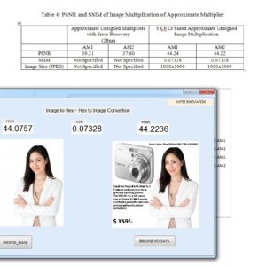
Low-Power Approximate Unsigned Multipliers with Configurable Error Recovery
Abstract:
Approximate circuits have been considered for applications that can tolerate some loss of accuracy with improved performance and/or energy efficiency. Multipliers are key arithmetic circuits in many of these applications including digital signal processing (DSP). In this paper, a novel approximate multiplier with a low power consumption and a short critical path is proposed for high-performance DSP applications. This multiplier leverages a newly designed approximate adder that limits its carry propagation to the nearest neighbors for fast partial product accumulation. Different levels of accuracy can be achieved by using either OR gates or the proposed approximate adder in a configurable error recovery. The multipliers using these two error reduction strategies are referred to as approximate multiplier 1 (AM1) and approximate multiplier 2 (AM2), respectively. Both AM1 and AM2 have a low mean error distance, i.e., most of the errors are not significant in magnitude. Compared to a Wallace multiplier optimized for speed, an 8×8 AM1 with 4 MSBs (most significant bits) for error reduction and synthesized using a 28 nm CMOS process shows a 60% reduction in delay (when optimized for delay) and a 42% reduction in power dissipation (when optimized for area). In a 16×16 design, half of the least significant partial products are truncated for AM1 and AM2, which are thus denoted as TAM1 and TAM2, respectively. Compared with the Wallace multiplier, TAM1 and TAM2 save from 50% to 66% in power, when optimized for area. Compared to existing approximate multipliers, AM1, AM2, TAM1 and TAM2 show significant advantages in accuracy with a high performance. AM2 has a better accuracy compared to AM1 but with a longer delay and higher power consumption. Image processing applications including image sharpening and smoothing are considered to show the quality of the approximate multipliers in error-tolerant applications. By utilizing an appropriate error recovery, the proposed approximate multipliers achieve similar processing accuracy as traditional exact multipliers, but with significant improvements in power.
List of the following materials will be included with the Downloaded Backup:
FIR Filter Design based on FPGA
Abstract:
FIR (Finite Impulse Response) Filters: the finite impulse response filter is the most basic components in digital signal processing systems are widely used in communications, image processing, and pattern recognition. Based on FPGA(editable logic device) to achieve FIR filter, not only take into account the fixed -function DSP-specific chip real-time, but also has the DSP processor flexibility. The combination of FPGA and DSP technology can further improve integration, increase work speed and expand system capabilities.
List of the following materials will be included with the Downloaded Backup:
An Efficient VLSI Architecture for Convolution Based DWT Using MAC
Abstract:
The modern real time applications related to image processing and etc., demand high performance discrete wavelet transform (DWT). This paper proposes the floating point multiply accumulate circuit (MAC) based 1D/2D-DWT, where the MAC is used to find the outputs of high/low pass FIR filters. The proposed technique is implemented with 45 nm CMOS technology and the results are compared with various existing techniques. The proposed 8 × 8-point floating point 2-levels 2D-DWT achieves 27.6% and 83.7% of reduction in total area and net power respectively as compared with existing DWT.
List of the following materials will be included with the Downloaded Backup:
Dual Quality 4:2 Compressor for Utilizing in Dynamic Accuracy Configurable Multipliers
Abstract:
In this paper, we propose four 4:2 compressors, which have the flexibility of switching between the exact and approximate operating modes. In the approximate mode, these dual-quality compressors provide higher speeds and lower power consumptions at the cost of lower accuracy. Each of these compressors has its own level of accuracy in the approximate mode as well as different delays and power dissipations in the approximate and exact modes. Using these compressors in the structures of parallel multipliers provides configurable multipliers whose accuracies (as well as their powers and speeds) may change dynamically during the runtime. The proposed multiplier saves few adder circuits in partial products, and this proposed multiplier is evaluated with an image processing application. In existing thing, to using this multiplier to design image processing evaluation on only luminance based application, but here the proposed work is modified with Gaussian noise reduction with luminance and chrominance based application, this design to implemented in VHDL, and synthesized in Xilinx S6LX9 FPGA and shown the power, area and delay reports.
List of the following materials will be included with the Downloaded Backup:
Design of Power and Area Efficient Approximate Multipliers
Abstract:
Approximate computing can decrease the design complexity with an increase in performance and power efficiency for error resilient applications. This brief deals with a new design approach for approximation of multipliers. The partial products of the multiplier are altered to introduce varying probability terms. Logic complexity of approximation is varied for the accumulation of altered partial products based on their probability. The proposed approximation is utilized in two variants of 16-bit multipliers. Synthesis results reveal that two proposed multipliers achieve power savings of 72% and 38%, respectively, compared to an exact multiplier. They have better precision when compared to existing approximate multipliers. Mean relative error figures are as low as 7.6% and 0.02% for the proposed approximate multipliers, which are better than the previous works. Performance of the proposed multipliers is evaluated with an image processing application, where one of the proposed models achieves the highest peak signal to noise ratio.
List of the following materials will be included with the Downloaded Backup:
Low Power FPGA Design Using Memoization Based Approximate Computing
Field-programmable gate arrays (FPGAs) are increasingly used as the computing platform for fast and energy efficient execution of recognition, mining, and search applications. Approximate computing is one promising method for achieving energy efficiency. Compared with most prior works on approximate computing, which target approximate processors and arithmetic blocks, this paper presents an approximate computing methodology for FPGA-based design. It studies memoization as a method for approximation on FPGA and analyzes different architectural and design parameters that should be considered. The proposed design flow leverages on high-level synthesis to enable memoization-based microarchitecture generation, thus also facilitating a C-to-register-transfer-level synthesis. When compared with the previous approaches of bit-width truncation and approximate multipliers, memoization-based approximate computation on FPGA achieves a significant dynamic power saving (around 20%) with very small area overhead (<5%) and better power-to-signal noise ratio values for the studied image processing benchmarks. The proposed architecture of this paper is verified using vivado HLS..
List of the following materials will be included with the Downloaded Backup:
Design and Analysis of a Majority Logic Based Imprecise 6-2 Compressor for Approximate Multipliers
Base Paper Abstract:
Approximate computing is an emerging paradigm for trading off computing accuracy to reduce energy consumption and design complexity in a variety of applications, for which exact computation is not a critical requirement. Different from conventional designs using AND-OR and XOR gates, the majority gate is widely used in many emerging nanotechnologies. An ultra-efficient 6-2 compressor is proposed in this paper. It is composed of two majority gates that lead to low energy consumption and high hardware efficiency. The proposed compressor is utilized in the approximate partial product reduction of a modified 8×8 Dadda multiplier with a truncated structure. Experimental results show that this multiplier realizes a significant reduction in hardware cost, especially in terms of power and area, on average by up to 40% and 31% respectively, compared to exact and state-of-the-art designs. The application of image multiplication is also presented to assess the practicability of the multiplier. The results show that the proposed multiplier results in images with higher quality in peak signal to noise ratio (PSNR) and mean structural similarity index metric (MSSIM) compared to other designs.
List of the following materials will be included with the Downloaded Backup:
Comparison and Extension of Approximate 4-2 Compressors for Low-Power Approximate Multipliers
Abstract:
Approximate multipliers attract a large interest in the scientific literature that proposes several circuits built with approximate 4-2 compressors. Due to the large number of proposed solutions, the designer who wishes to use an approximate 4-2 compressor is faced with the problem of selecting the right topology. In this paper, we present a comprehensive survey and comparison of approximate 4-2 compressors previously proposed in literature. We present also a novel approximate compressor, so that a total of twelve different approximate 4-2 compressors are analyzed. The investigated circuits are employed to design 8 × 8 and 16 × 16 multipliers, implemented in 28nm CMOS technology. For each operand size we analyze two multiplier configurations, with different levels of approximations, both signed and unsigned. Our study highlights that there is no unique winning approximate compressor topology since the best solution depends on the required precision, on the signedness of the multiplier and on the considered error metric.
List of the following materials will be included with the Downloaded Backup:
Area-Time Efficient Streaming Architecture for FAST and BRIEF Detector
Abstract:
The combination of FAST corners and BRIEF descriptors provide highly robust image features. We present a novel detector for computing the FAST-BRIEF features from streaming images. To reduce the complexity of the BRIEF descriptor, we employ an optimized adder tree to perform summation by accumulation on streaming pixels for the smoothing operation. Since the window buffer used in existing designs for computing the BRIEF point-pairs are often poorly utilized, we propose an efficient sampling scheme that exploits register reuse to minimize the number of registers. Synthesis results based on 65- nm CMOS technology show that the proposed FAST-BRIEF core achieves over 40% reduction in area-delay product compared to the baseline design. In addition, we show that the proposed architecture can achieve 1.4x higher throughput than the baseline architecture with slightly lower energy consumption.
List of the following materials will be included with the Downloaded Backup:
Area-Efficient Bidirectional Shift-Register Using Bidirectional Pulsed-Latches
Abstract:
This paper proposes an area-efficient bidirectional shift-register using bidirectional pulsed-latches. The proposed bidirectional shift-register reduces the area and power consumption by replacing master-slave flip-flops and 2-to-1 multiplexers with the proposed bidirectional pulsed-latches and non-overlap delayed pulsed clock signals, and by using sub shift-registers and extra temporary storage latches. A 256-bit bidirectional shift-register was fabricated using a 65nm CMOS process. Its area was 1,943μm2 and its power consumption is 200μW at a 100MHz clock frequency with VDD=1.2V. It reduces area by 39.2% and power consumption by 19.4% compared to the conventional bidirectional shift-register, length in most cases.
List of the following materials will be included with the Downloaded Backup:
A 16-bit 2.0-ps Resolution Two-Step TDC in 0.18-μm CMOS Utilizing Pulse-Shrinking Fine Stage
Abstract:
This paper proposes a time-to-digital converter (TDC) that achieves wide input range and fine time resolution at the same time. The proposed TDC utilizes pulse-shrinking (PS) scheme in the second stage for a fine resolution and two-step (TS) architecture for a wide range. The proposed PS TDC prevents an undesirable non-uniform shrinking rate issue in the conventional PS TDCs by utilizing a built-in offset pulse and an offset pulse width detection schemes. With several techniques, including a built-in coarse gain calibration mechanism, the proposed TS architecture overcomes a nonlinearity due to the signal propagation and gain mismatch between coarse and fine stages. The simulation results of the TDC implemented in a 0.18-µm standard CMOS technology demonstrate 2.0-ps resolution and 16-bit range that corresponds to ∼130-ns input time interval with 0.08-mm2 area. It operates at 3.3 MS/s with 18.0 mW from 1.8-V supply and achieves 1.44-ps single-shot precision. Index Terms— Built-in calibration, pulse shrinking (PS), time-to-digital conversion, two step (TS).
List of the following materials will be included with the Downloaded Backup:
Efficient Super Resolution Algorithm using Overlapping Bi-cubic Interpolation
Abstract:
In practical CCTV applications, there are problems of the camera with low resolution, camera fields of view, and lighting environments. These could degrade the image quality and it is difficult to extract useful information for further processing. Super-resolution techniques have been proposed widely by the researchers. However, many approaches are complex and are difficult to use in practical scenarios. In this paper, we propose an efficient Super-resolution algorithm using overlapping bi-cubic for hardware implementation. Experimental results are verified using processing time and reconstructed images that can be used in real time applications.
List of the following materials will be included with the Downloaded Backup:
Design and Low-Complexity Implementation of Matrix–Vector Multiplier for Iterative Methods in Communication Systems
Abstract: Iterative methods are basic building blocks of communication systems and often represent a dominating part of the system, and therefore, they necessitate careful design and implementation for optimal performance. In this brief, we propose a novel field programmable gate arrays design of matrix–vector multiplier that can be used to efficiently implement widely adopted iterative methods. The proposed design exploits the sparse structure of the matrix as well as the fact that spreading code matrices have equal magnitude entries. Implementation details and timing analysis results are promising and are shown to satisfy most modern communication system requirements.
List of the following materials will be included with the Downloaded Backup:
Parallel Pipelined Architecture and Algorithm for Matrix Transposition Using Registers
Base Paper Abstract:
In this brief, we present a new algorithm and architecture for continuous-flow matrix transposition using registers. The algorithm supports P-parallel matrix transposition. The hardware architecture reaches the theoretical minimums in terms of latency and memory. It is composed of a group of identical cascaded basic swap circuits, whose stages are determined by the corresponding algorithm, and can be controlled via a set of counters. Compared with the state-of-the-art architecture, the proposed architecture supports matrices whose rows and columns are integer multiples of P. Here P can be arbitrary, including but not limited to power-of-two integers. Moreover, our results provide additional insight into continuous-flow non-square matrix transposition.
List of the following materials will be included with the Downloaded Backup:
MInSC: A VLSI Architecture for Myocardial Infarction Stages Classifier for Wearable Healthcare Applications
Base Paper Abstract:
Myocardial Infarction (MI) is a critical heart abnormality causing millions of fatalities worldwide every year. MI progress in three stages based on its severity causing several changes in an Electrocardiogram (ECG) signal. It is very critical to capture these variations, which requires continuous monitoring of the ECG signal of the patient. Therefore, it becomes imperative to develop a low power VLSI architecture to address the prognosis of MI. In this brief, for the first time, an area and power efficient design of a five stage classifier is proposed, which detects the progression of various stages of MI using ECG beats in real time. The proposed architecture has an area and total power utilization of 1.38mm2 and 5.12µW, respectively at SCL 180nm Bulk CMOS technology. The low power and area requirements and multiclass classification capability of the proposed design make it suitable to be used in wearable devices.
List of the following materials will be included with the Downloaded Backup:
Fast and Hardware-Efficient Variable Step Size Adaptive Beamformer
Base Paper Abstract:
Constant step size least mean square (CSS-LMS) is one of the most popular adaptive beamforming algorithms. However, for varying channel signal-to-noise ratios (SNRs), the CSS algorithms are not effective, and there is a need for variable step size (VSS) algorithms. The VSS algorithms provide extremely deep nulls for the interferences; however, they are complex to implement on hardware. Hence, this paper proposes two hardware-efficient variable step size algorithms, namely, efficient variable step size LMS (EVSS-LMS) and reduced complexity parallel LMS (EVSS-RC-pLMS). The proposed EVSS algorithms eliminate the complex operations of VSS algorithms like division and exponential and approximate them to simpler operations. Further, MATLAB simulations demonstrate accelerated convergence, deep nulls, a lower error floor, and better performance in varying SNR environments for the proposed algorithms. Additionally, the finite precision radiation patterns are similar to infinite precision. Hardware synthesis results show the outstanding performance of EVSS in terms of resource utilization on the Xilinx Artix-7 FPGA.
List of the following materials will be included with the Downloaded Backup:
Design of High Speed 8-bit Vedic Multiplier using Brent Kung Parallel Prefix Adder
Base Paper Abstract:
One of the primary purposes of a digital signal processing system is multiplication. The multiplier’s performance affects the DSP system’s overall performance. Therefore, it is crucial to create an effective and quick multiplier implementation design. Vedic mathematics can be used to simplify complex computations so that they are easier to perform verbally. Urdhva Triyambakam is the multiplication algorithm used in Vedic math. In this paper, we employing Brent Kung adder to enhance the Vedic multiplier’s performance. The Urdhva Tiryagbhyam sutra is being used in place of other multiplication strategies since it applies to all instances of algorithms for N x N bit numbers and produces the least amount of latency. Four 4-bit vedic multipliers, two 8-bit Brent Kung adders, one 4-bit Brent Kung adder, and an OR gate are used to create an 8-bit vedic multiplier. A 4-bit vedic multiplier is created similarly by combining four 2-bit vedic multipliers, two 4-bit Brent Kung Adders, one 2-bit Brent Kung Adder, and one OR gate. These four-bit vedic multipliers are then combined to form an eight-bit vedic multiplier. After that, Xilinx Vivado Software is used to simulate and synthesis the 8 x 8 Vedic Multiplier, which was coded in Verilog HDL. The proposed Vedic Multiplier is outperformed in terms of speed when compared to related works.
List of the following materials will be included with the Downloaded Backup:
An Optimization in Conventional Shift &Add Multiplier for Area-Efficient Implementation on FPGA
Base Paper Abstract:
FPGA is familiar with prototyping and implementing simple to complex DSP systems. The FPGA based design may be highly affected by factors that include selection of an FPGA board, Electronic Design Automation Tool and the Programming Techniques to optimize the algorithm. The algorithm optimization results in a more compact design regarding the area and achieved frequency. In DSP algorithms optimization, the major bottleneck is the multiplier complexity evident in, for example - FIR, IIR, FFT, and others. Research shows much work on multiplier optimization. Despite all possible optimization techniques, the multiplier consumes tremendous resources when translated on hardware, with more power consumption and observed delay. The proposed work is novel in that it brings resources optimization in a familiar shift and add multiplier algorithm by implementing the design in FPGA and comparing the results with the existing shift, and add a multiplier. In the implementation of the design, Xilinx Vertex -7 FPGA is used along with ISE 14.2 simulators. The parameters to compare are the Lookup tables (Logic element of FPGA), adder/subtractors and the multiplexers, along with performance characters, like the operating frequency, delay and total levels of logic (path travelled by the signal in register transfer level). The output shows that the anticipated design is an excellent alternative to the conventional shift and add algorithm.
List of the following materials will be included with the Downloaded Backup:
FPGA Implementation of TFT 1.8 inch SPI 128×160 Display ROM Interface
Simple Description:
This ST7735R is a display controller used in small TFT (Thin-Film Transistor) LCD displays. It is often used in combination with microcontrollers or FPGAs to drive these displays. The controller supports the Serial Peripheral Interface mode of communication for sending commands and data to the display. This TFT display helps with a greater number of image and video processing applications. Here we have implemented this TFT display in FPGA hardware implementation using Verilog HDL with a novelty-based architecture design. Finally shown the output with TFT Display.
List of the following materials will be included with the Downloaded Backup:
Hybrid Protection of Digital FIR Filters
Base Paper Abstract:
A digital finite impulse response (FIR) filter is a ubiquitous block in digital signal processing applications and its behavior is determined by its coefficients. To protect filter coefficients from an adversary, efficient obfuscation techniques have been proposed, either by hiding them behind decoys or replacing them by key bits. In this article, we initially introduce a query attack that can discover the secret key of such obfuscated FIR filters, which could not be broken by the existing prominent attacks. Then, we propose a first of its kind hybrid technique, including both hardware obfuscation and logic locking using a point function for the protection of parallel direct and transposed forms of digital FIR filters. Experimental results show that the hybrid protection technique can lead to FIR filters with higher security while maintaining the hardware complexity competitive or superior to those locked by prominent logic locking methods. It is also shown that the protected multiplier blocks and FIR filters are resilient to existing attacks. The results on different forms and realizations of FIR filters show that the parallel direct form FIR filter has a promising potential for a secure design.
List of the following materials will be included with the Downloaded Backup:
Design and Implementation of Arithmetic Logic Unit in HDL
Proposed Abstract:
Arithmetic logic unit (ALU) is an important part of all digital gadgets and applications. This paper presents the design and implementation of an 8-bit Arithmetic Logic Unit (ALU) with a capability to perform eight distinct operations. ALUs are fundamental components in the central processing units (CPUs) of microprocessors and are responsible for executing arithmetic and logical operations. The primary objective of this research is to design an efficient and versatile 8-bit ALU that can execute a wide range of operations while optimizing for performance and area efficiency. The proposed 8-bit ALU is designed to perform the following eight operations: Ripple carry addition, Ripple borrow subtraction, Array multiplication, XOR operation, left shift, right shift, NAND operation and a logical NOR operation. The research presents a detailed description of the ALU's architecture, its constituent components, and the control mechanism for selecting operations. Performance metrics, such as speed, area efficiency, and power consumption, are analyzed and compared with Xilinx FPGA.
List of the following materials will be included with the Downloaded Backup:
Low power Dadda multiplier using approximate almost full adder and Majority logic based adder compressors
Base Paper Abstract:
An Approximate computing is widely used to have energy-efficient system design in Very Large-Scale Integration (VLSI). This approach is best suited for signal processing and multimedia applications where low power consumption is the main concern. Faster and significant results can be obtained from an approximate computing at the cost of reduced accuracy. In this work, we proposed a very novel design approaches based on various monolithic 4:2 compressors. Proposed approach is applied to have reduced stages in the partial product multiplication. Proposed Monolithic compressor had outperformed over various 4:2 compressors. Our proposed method is based on majority logic based with the use of Dadda multiplication. A new-partial product reduction format is implemented by this multiplier, which reduces the maximum output delay. This method of approach significantly reduces the utilization of number of MOSFETs compared to other multiplier such as Wallace Tree Multipliers. Simulation results are compared with conventional Dadda multiplier and ML based 4:2 compressors. Proposed approximate computing based almost full adder based majority logic based Dadda multiplier achieves reduction of 60.93% in area utilization 72.48% reduction in dynamic power reduction while processing time is also reduced by 72.98%. Dadda multiplication outperforms the other compressors.
List of the following materials will be included with the Downloaded Backup:
Hamming based Single Fault Error Correction Code
Proposed Abstract:
Signal processing and communication systems often use digital filters. In certain circumstances, the dependability of such systems is essential, prompting the construction of fault-tolerant filters. Many methods that take use of the structure and characteristics of the filters to achieve fault tolerance have been put forward throughout the years. Technology advances permit more intricate systems with several filters. It is typical for some of the filters in such complicated systems to function in simultaneously, for instance by using the same filter on several input signals. Recently, a straightforward method for achieving fault tolerance was given that takes use of the existence of parallel filters. This paper expands on that concept to demonstrate how error correction codes (ECCs), in which each filter is the equivalent of a bit in a conventional ECC, may be used to secure parallel filters. When there are several parallel filters operating simultaneously, this new technique enables more effective protection. The efficiency of the method in terms of protection and implementation cost is assessed using a case study of parallel finite impulse response filters.
List of the following materials will be included with the Downloaded Backup:
FPGA Implementation of 8×8 Truncated Multiplier
Proposed Abstract:
The operation of multiplication is an often encountered need in the field of digital signal processing. Parallel multipliers provide a rapid approach for performing multiplication operations, while demanding a significant amount of space in VLSI (Very Large Scale Integration) implementations. In the majority of signal processing applications, there is a preference for using a rounded result in order to prevent an increase in the size of the word. Therefore, an important goal in the design process is to minimize the spatial demand of the rounded output multiplier. This study introduces a novel approach to parallel multiplication that efficiently calculates the products of two n-bit values by selectively summing the most important columns using a variable correction technique. This research furthermore includes a comparative analysis of the implementation of 8X8 conventional and truncated multipliers using Verilog Hardware Description Language (HDL) on Field Programmable Gate Arrays (FPGAs). The shortened multiplier demonstrates a much greater decrease in device consumption as compared to the regular multiplier. A conventional multiplier performs computations on n x n bits and produces a weighted sum of the output, consisting of 2n bits. In contrast, a truncated multiplier generates an output of just n bits from the n x n bit input. The use of logic gates in both internal and external hardware design will be decreased. Truncated multipliers provide a viable approach for achieving significant reductions in FPGA resources, latency, and power consumption compared to regular parallel multipliers, particularly in scenarios where the complete accuracy provided by the standard multiplier is unnecessary.
List of the following materials will be included with the Downloaded Backup:
Design of SEU Tolerant 2D-FFT in SRAM-based FPGA
Base Paper Abstract:
2-Dimensional fast Fourier transform (FFT) has been widely used in radar signal process. Due to the need for high performance, field programmable gate array (FPGA) is an ideal hardware device for this application. For space-borne radar platform such as synthetic aperture radar (SAR), single-event upsets (SEUs) can cause lots of soft errors in static random access memory (SRAM) based FPGA. As to this, protecting the 2D-FFT implemented in FPGA from SEUs is very important. In this article, we analyze the critical weakness induced by SEUs in the 2D-FFT process, and then a 2D-FFT design with high SEU resilience is presented. The design utilizes the advantage of several anti-SEU methods. For butterfly control in FFT, partially triple modular redundancy (TMR) is used. For data buffers, error correction code (ECC) is applied to read and write operation. Furthermore, safe finite state machine (FSM) is adopted by important control registers. Fault injection results show that all these reinforcement technologies contribute to enhance the ability to mitigate the SEU effects.
List of the following materials will be included with the Downloaded Backup:
FPGA Implementation of D8PSK Demodulator
Base Paper Abstract:
Differential phase shift keying (DPSK) is a modulation scheme that facilitates non coherent demodulation and is employed for various applications such as Wireless Local Area Networks (WLANs), Bluetooth and RFID communication. In this paper, design, development and hardware implementation of a new demapping scheme for Differential 8-PSK (D8PSK) demodulator on a Zynq 7000 FPGA based ZED board is proposed using the concepts of model based design. The proposed work can be easily extended to other M-ary DPSK schemes.
List of the following materials will be included with the Downloaded Backup:
ReAdapt: A Reconfigurable Datapath for Runtime Energy-Quality Scalable Adaptive Filters
Base Paper Abstract:
This paper proposes ReAdapt–a reconfigurable datapath architecture for scaling the energy-quality trade-off of adaptive filtering at runtime. The ReAdapt can dynamically select four adaptive filtering algorithms for gradating complexity levels during runtime by reconfiguring the processing flow in its datapath and by blocking the switching activity (e.g., reducing the CMOS dynamic power) of unused modules with data-gating. The ReAdapt proposal can scale the energy-quality trade-off by choosing the following four different levels of filter algorithms complexity: 1) least mean square (LMS); 2) partial update normalized LMS (PU-NLMS); 3) set-membership normalized LMS (SM-NLMS); 4) normalized LMS (NLMS). The ReAdapt architecture reuses common modules of each adaptive filter, resulting in a compact VLSI hardware implementation. The ReAdapt architecture operation is implemented in a case-study for interference mitigation for electroencephalogram (EEG) signal processing. The hardware synthesis results show an increase of 6.80 times in throughput and at least a reduction of 2.84 times in energy per operation compared with the state-of-the-art adaptive filters. This paper also investigates the benefits of dynamically reconfiguring the four ReAdapt operating modes at runtime for different levels of signal-to-noise ratio (SNR) for the processed signals. We also demonstrate that dynamically reconfiguring the ReAdapt operating modes during runtime results in an optimal energy-quality trade-off which is advantageous over the conventional single static mode.
List of the following materials will be included with the Downloaded Backup:
AxPPA: Approximate Parallel Prefix Adders
Base Paper Abstract:
Addition units are widely used in many computational kernels of several error-tolerant applications such as machine learning and signal, image, and video processing. Besides their use as stand-alone, additions are essential building blocks for other math operations such as subtraction, comparison, multiplication, squaring, and division. The parallel prefix adders (PPAs) is among the fastest adders. It represents a parallel prefix graph consisting of the carry operator nodes, called prefix operators (POs). The PPAs, in particular, are among the fastest adders because they optimize the parallelization of the carry generation (G) and propagation (P). In this work, we introduce approximate PPAs (AxPPAs) by exploiting approximations in the POs. To evaluate our proposal for approximate POs (AxPOs), we generate the following AxPPAs, consisting of a set of four PPAs: approximate Brent–Kung (AxPPA-BK), approximate Kogge–Stone (AxPPAKS), Ladner-Fischer (AxPPA-LF), and Sklansky (AxPPA-SK). We compare four AxPPA architectures with energy-efficient approximate adders (AxAs) [i.e., Copy, error-tolerant adder I (ETAI), lower-part OR adder (LOA), and Truncation (trunc)]. We tested them generically in stand-alone cases and embedded them in two important signal processing application kernels: a sum of squared differences (SSDs) video accelerator and a finite impulse response (FIR) filter kernel. The AxPPA-LF provides a new Pareto front in both energy-quality and area-quality results compared to state-of-the-art energy-efficient AxAs.
List of the following materials will be included with the Downloaded Backup: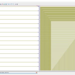
Power Efficient Tiny Yolo CNN Using Reduced Hardware Resources Based on Booth Multiplier and WALLACE Tree Adders
Base Paper Abstract:
Convolutional Neural Network (CNN) has attained high accuracy and it has been widely employed in image recognition tasks. In recent times, deep learning-based modern applications are evolving and it poses a challenge in research and development of hardware implementation. Therefore, hardware optimization for efficient accelerator design of CNN remains a challenging task. A key component of the accelerator design is a processing element (PE) that implements the convolution operation. To reduce the amount of hardware resources and power consumption, this article provides a new processing element design as an alternate solution for hardware implementation. Modified BOOTH encoding (MBE) multiplier and WALLACE tree-based adders are proposed to replace bulky MAC units and typical adder tree respectively. The proposed CNN accelerator design is tested on Zynq-706 FPGA board which achieves a throughput of 87.03 GOP/s for Tiny-YOLO-v2 architecture. The proposed design allows to reduce hardware costs by 24.5% achieving a power efficiency of 61.64 GOP/s/W that outperforms the previous designs.
List of the following materials will be included with the Downloaded Backup: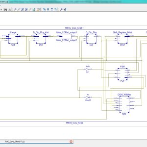
A High-Speed FPGA-based True Random Number Generator using Metastability with Clock Managers
Base Paper Abstract:
True random number generators (TRNGs) are fundamentals in many important security applications. Though they exploit randomness sources that are typical of the analog domain, digital-based solutions are strongly required especially when they have to be implemented on Field Programmable Gate Array (FPGA)-based digital systems. This paper describes a novel methodology to easily design a TRNG on FPGA devices. It exploits the runtime capability of the Digital Clock Manager (DCM) hardware primitives to tune the phase shift between two clock signals. The presented auto-tuning strategy automatically sets the phase difference of two clock signals in order to force on one or more flip-flops (FFs) to enter the metastability region, used as a randomness source. Moreover, a novel use of the fast carry-chain hardware primitive is proposed to further increase the randomness of the generated bits. Finally, an effective on-chip post-processing scheme that does not reduce the TRNG throughput is described. The proposed TRNG architecture has been implemented on the Xilinx Zynq XC7Z020 System on Chip (SoC). It passed all the National Institute of Standards and Technology (NIST) SP 800-22 statistical tests with a maximum throughput of 300×106 bit per second. The latter is considerably higher than the throughput of other previously published DCMbased TRNGs.
List of the following materials will be included with the Downloaded Backup: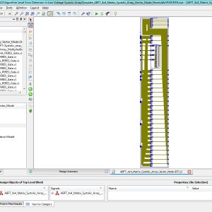
Algorithm Level Error Detection in Low Voltage Systolic Array
Base Paper Abstract:
In this brief an approach is proposed to achieve energy savings from reduced voltage operation. The solution detects timing-errors by integrating Algorithm Based Fault Tolerance (ABFT) into a digital architecture. The approach has been studied with a systolic array matrix multiplier operating at reduced voltages, detecting errors on-the-fly to avoid energy demanding memory round-trips. The analysis of the solution has been done using analog-digital co-simulation to extract the transient behavior under different voltages and clock frequencies. HSPICE simulations using 90nm CMOS transistor models, and experiments by reducing operation voltage of an FPGA device were carried out. HSPICE simulations, showed possibility of 10x increase in energy-efficiency by approaching near-threshold region.
List of the following materials will be included with the Downloaded Backup: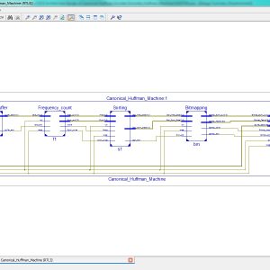
A High-Throughput VLSI Architecture Design of Canonical Huffman Encoder
Abstract:
In this brief, a high-throughput Huffman encoder VLSI architecture based on the Canonical Huffman method is proposed to improve the encoding throughput and decrease the encoding time required by the Huffman code word table construction process. We proposed parallel computing architectures for frequency-statistical sorting and code-size computational sorting. This architecture results in a process of building a tree and assigning symbols that can be completed by scanning the data only once. This solves the problem of the low efficiency of the traditional algorithm, which needs to scan the data twice. Consequently, in addition to the advantages of the high compression ratio inherited from the Canonical Huffman, the proposed architecture has overridden advantages for a high parallelism processing capacity. The experimental results showed that the proposed architecture decreased the encoding time by 26.30% compared to the available Huffman encoder using the standard algorithm when encoding 256 8-bit symbols. Furthermore, the VLSI architecture could further decrease the encoding time when encoding more 8-bit symbols. In particular, when encoding 212,642 8-bit symbols, the proposed VLSI architecture could reduce the encoding time by 87.40%. Thus, compared with the traditional Huffman encoders, this brief achieved the improvement of coding efficiency.
List of the following materials will be included with the Downloaded Backup:
High Performance Accurate and Approximate Multipliers for FPGA based Hardware Accelerators
Abstract:
Multiplication is one of the widely used arithmetic operations in a variety of applications, such as image/video processing and machine learning. FPGA vendors provide high performance multipliers in the form of DSP blocks. These multipliers are not only limited in number and have fixed locations on FPGAs but can also create additional routing delays and may prove inefficient for smaller bit-width multiplications. Therefore, FPGA vendors additionally provide optimized soft IP cores for multiplication. However, in this work, we advocate that these soft multiplier IP cores for FPGAs still need better designs to provide high-performance and resource efficiency. Towards this, we present generic area-optimized, low-latency accurate and approximate soft-core multiplier architectures, which exploit the underlying architectural features of FPGAs, i.e., look-up table (LUT) structures and fast carry chains to reduce the overall critical path delay and resource utilization of multipliers. Compared to Xilinx multiplier LogiCORE IP, our proposed unsigned and signed accurate architecture provides up to 25% and 53% reduction in LUT utilization, respectively, for different sizes of multipliers. Moreover, with our unsigned approximate multiplier architectures, a reduction of up to 51% in the critical path delay can be achieved with an insignificant loss in output accuracy when compared with the LogiCORE IP. For illustration, we have deployed the proposed multiplier architecture in accelerators used in image and video applications, and evaluated them for area and performance gains.
List of the following materials will be included with the Downloaded Backup:
FPGA Based High Definition SPWM Generation With Harmonic Mitigation Property
Abstract:
High-resolution sinusoidal pulse width modulation (SPWM) switching is beneficial in order to achieve compact size and fine sinusoidal output of dc–ac converters. In this article, a novel field-programmable gate array (FPGA) based high-definition SPWM (HD-SPWM) architecture is proposed for adopting a scheme of integrating a lower frequency PWM train to a high-frequency SPWM train in order to suppress inverter output harmonics while achieving high resolution output. An optimized FPGA based two-stage finite-state-machine (FSM) architecture is designed, where the initial stage decides pulse widths of a lower frequency PWM train based on the premeditated pulse width of the high-frequency SPWM train, whereas in the final stage, lower frequency PWM pulse widths are integrated with the high-frequency SPWM pulse widths to generate updated pulse widths of high-frequency SPWM, i.e., HD-SPWM. Moreover, a pre-formulation mathematical model is established for the calculation of duty-cycle count values of pulse trains to support the online adjustment of modulation index (MI) of the HD-SPWM. The proposed generation has the benefits of harmonic mitigation, online fine adjustment of MI, low-processing time, and requirement of a minor segment of a medium-sized FPGA; thereby, providing a good tradeoff between larger designs and higher performance. Theoretical calculations, characteristics, and design contemplations are specified, and the HD-SPWM generation is demonstrated through experimentation with a Xilinx Spartan-3 FPGA board.
List of the following materials will be included with the Downloaded Backup:
Implementation of Low Power 1-bit Hybrid Full Adder using 22nm CMOS Technology
Abstract:
Adders are plays a vital role in digital and vlsi systems. Arithmetic operations are an essential part of digital systems. During VLSI systems, the entire research is on lowering the scale of transistors for enforcing any other digital system. This proposed architecture implemented by different types of logic systems; each logic performs the different role in the hybrid system. The hybrid Full Adder cell with one bit is implemented in this structure. The proposed method is investigated using 22-nm CMOS hybrid full adder. The proposed architecture demonstrates substantial efficiency in power consumption and delay, based on simulation results. The simulation result expressed that the full adder circuit is used to modern high speed central processing unit in the data path architecture. This form of hybrid Full Adder, reduces the delay and increasing efficiency and mainly used in nano technology applications. The average power consumption of 1.1055uW with moderately low delay of 7.0415 ps was found to be extremely low for 0.8-V supply at 22-nm technology. These kind of adder allocates significant improvements in power, high speed and area compared with previous full adder designs.
List of the following materials will be included with the Downloaded Backup:Provide Wordlwide Online Support
We can provide Online Support Wordlwide, with proper execution, explanation and additionally provide explanation video file for execution and explanations.
24/7 Support Center
NXFEE, will Provide on 24x7 Online Support, You can call or text at +91 9789443203, or email us nxfee.innovation@gmail.com
Terms & Conditions:
Customer are advice to watch the project video file output, and before the payment to test the requirement, correction will be applicable.
After payment, if any correction in the Project is accepted, but requirement changes is applicable with updated charges based upon the requirement.
After payment the student having doubts, correction, software error, hardware errors, coding doubts are accepted.
Online support will not be given more than 3 times.
On first time explanation we can provide completely with video file support, other 2 we can provide doubt clarifications only.
If any Issue on Software license / System Error we can support and rectify that within end of day.
Extra Charges For duplicate bill copy. Bill must be paid in full, No part payment will be accepted.
After payment, to must send the payment receipt to our email id.
Powered by NXFEE INNOVATION, Pondicherry.
Call us today at : +91 9789443203 or Email us at nxfee.innovation@gmail.com
NXFEE Development & Services

Product Categories
- 2014 (12)
- 2015 (39)
- 2016 (31)
- 2017 (16)
- 2018 (17)
- 2019 (42)
- 2020 (29)
- 2021 (16)
- 2022 (22)
- 2023 (17)
- Area Efficient (92)
- High speed VLSI Design (49)
- IEEE (16)
- Image Processing (34)
- Low power VLSI Design (71)
- NOC VLSI Design (3)
- VLSI (180)
- VLSI Application / Interface and Mini Projects (13)
- VLSI_2023 (15)
Filter by price
Product Status
Sort by producents

Copyright © 2021 Nxfee Innovation.