50 Products found
Approximate Pruned and Truncated Haar Discrete Wavelet Transform VLSI Hardware for Energy-Efficient ECG Signal Processing
Abstract:
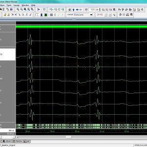
The approximate computing paradigm emerged as a key alternative for trading off accuracy and energy efficiency. Error-tolerant applications, such as multimedia and signal processing, can process the information with lower-than-standard accuracy at the circuit level while still fulfilling a good and acceptable service quality at the application level. The automatic detection of R-peaks in an electrocardiogram (ECG) signal is the essential step preceding ECG processing and analysis. The Haar discrete wavelet transform (HDWT) is a low-complexity pre-processing filter suitable to detect ECG R-peaks in embedded systems like wearable devices, which are incredibly energy constrained. This work presents an approximate HDWT hardware architecture for ECG processing at very high energy efficiency. Our best-proposal employing pruning within the approximate HDWT hardware architecture requires just seven additions. The use of a truncation technique to improve energy efficiency is also investigated herein by observing the evolution of the signal-to-noise ratio and the ultimate impact in the ECG peak-detection application. This research finds that our HDWT approximate hardware architecture proposal accepts higher truncation levels than the original HDWT. In summary: Our results show about 9 times energy reduction when combining our HDWT matrix approximation proposal with the pruning and the highest acceptable level of truncation while still maintaining the R-peak detection performance accuracy of 99.68% on average.
List of the following materials will be included with the Downloaded Backup: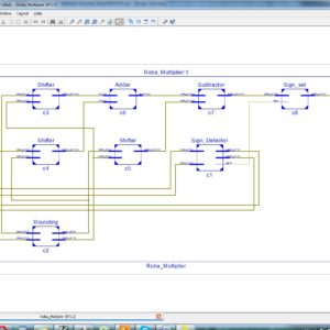
RoBA Multiplier A Rounding Based Approximate Multiplier for High Speed yet Energy Efficient Digital Signal Processing
Abstract:
In this paper, we propose an approximate multiplier that is high speed yet energy efficient. The approach is to round the operands to the nearest exponent of two. This way the computational intensive part of the multiplication is omitted improving speed and energy consumption at the price of a small error. The proposed approach is applicable to both signed and unsigned multiplications. We propose three hardware implementations of the approximate multiplier that includes one for the unsigned and two for the signed operations. The efficiency of the proposed multiplier is evaluated by comparing its performance with those of some approximate and accurate multipliers using different design parameters. In addition, the efficacy of the proposed approximate multiplier is studied in two image processing applications, i.e., image sharpening and smoothing.
List of the following materials will be included with the Downloaded Backup: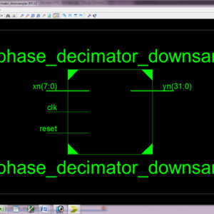
To develop and Implement Low Power, High Speed VLSI for Processing Signals using Multi rate Techniques Low Power Divider Using Vedic Mathematics
Abstract:
Multirate technique is necessary for systems with different input and output sampling rates. Recent advances in mobile computing and communication applications demand low power and high speed VLSI DSP systems. In this paper to discuss the downsampling technique and its improvement, major drawbacks of present approaches possible to increase degeneracy. This Multirate design methodology is systematic and applicable to many problems. The proposed architecture of this paper analysis the logic size, area and power consumption using Xilinx 14.2.The proposed architecture of this paper analysis the logic size, area and power consumption using Xilinx 14.2.
List of the following materials will be included with the Downloaded Backup: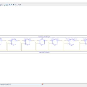
FPGA Heart Rate Monitoring (Pre Processing – QRS Detection Stage)
Base Paper Abstract:
The continuous monitoring of cardiac patients requires an ambulatory system that can automatically detect heart diseases. This study presents a new field programmable gate array (FPGA)-based hardware implementation of the QRS complex detection. The proposed detection system is mainly based on the Pan and Tompkins algorithm, but applying a new, simple, and efficient technique in the detection stage. The new method is based on the centered derivative and the intermediate value theorem, to locate the QRS peaks. The proposed architecture has been implemented on FPGA using the Xilinx System Generator for digital signal processor and the Nexys-4 FPGA evaluation kit. To evaluate the effectiveness of the proposed system, a comparative study has been performed between the resulting performances and those obtained with existing QRS detection systems, in terms of reliability, execution time, and FPGA resources estimation. The proposed architecture has been validated using the 48 half-hours of records obtained from the Massachusetts Institute of Technology - Beth Israel Hospital (MITBIH) arrhythmia database. It has also been validated in real time via the analogue discovery device.
List of the following materials will be included with the Downloaded Backup:
Vital-Sign Processing Receiver With Clutter Elimination Using Servo Feedback Loop for UWB Pulse Radar System
Abstract:
This brief presents a vital-sign processing circuit for simultaneous dc/near-dc elimination and out-of-band interference rejection without any digital signal processing or algorithm assistance for the ultra wideband (UWB) pulse-based radar system. An intrinsic self balanced MOS diode (SBMD) was proposed as a stable and balanced pseudo resistor applied under a servo feedback loop in a vital-sign receiver of the sensing radar to perform as a high-pass filter (HPF) with an ultralow corner frequency lower than 0.5 Hz for removing undesired clutters of the reflected signals and input dc-offset voltages from innate circuit offsets. A third-order switched-capacitor (SC) Chebyshev low-pass filter (LPF) with leap-frog topology as the subsequent stage was adopted to suppress the out-band noises, thereby establishing an integrated vital-sign processing circuit with band pass frequency response and incorporating it into a radar module to verify its viability.
List of the following materials will be included with the Downloaded Backup:
Design of High Speed 8-bit Vedic Multiplier using Brent Kung Parallel Prefix Adder
Base Paper Abstract:
One of the primary purposes of a digital signal processing system is multiplication. The multiplier’s performance affects the DSP system’s overall performance. Therefore, it is crucial to create an effective and quick multiplier implementation design. Vedic mathematics can be used to simplify complex computations so that they are easier to perform verbally. Urdhva Triyambakam is the multiplication algorithm used in Vedic math. In this paper, we employing Brent Kung adder to enhance the Vedic multiplier’s performance. The Urdhva Tiryagbhyam sutra is being used in place of other multiplication strategies since it applies to all instances of algorithms for N x N bit numbers and produces the least amount of latency. Four 4-bit vedic multipliers, two 8-bit Brent Kung adders, one 4-bit Brent Kung adder, and an OR gate are used to create an 8-bit vedic multiplier. A 4-bit vedic multiplier is created similarly by combining four 2-bit vedic multipliers, two 4-bit Brent Kung Adders, one 2-bit Brent Kung Adder, and one OR gate. These four-bit vedic multipliers are then combined to form an eight-bit vedic multiplier. After that, Xilinx Vivado Software is used to simulate and synthesis the 8 x 8 Vedic Multiplier, which was coded in Verilog HDL. The proposed Vedic Multiplier is outperformed in terms of speed when compared to related works.
List of the following materials will be included with the Downloaded Backup:
Hybrid Protection of Digital FIR Filters
Base Paper Abstract:
A digital finite impulse response (FIR) filter is a ubiquitous block in digital signal processing applications and its behavior is determined by its coefficients. To protect filter coefficients from an adversary, efficient obfuscation techniques have been proposed, either by hiding them behind decoys or replacing them by key bits. In this article, we initially introduce a query attack that can discover the secret key of such obfuscated FIR filters, which could not be broken by the existing prominent attacks. Then, we propose a first of its kind hybrid technique, including both hardware obfuscation and logic locking using a point function for the protection of parallel direct and transposed forms of digital FIR filters. Experimental results show that the hybrid protection technique can lead to FIR filters with higher security while maintaining the hardware complexity competitive or superior to those locked by prominent logic locking methods. It is also shown that the protected multiplier blocks and FIR filters are resilient to existing attacks. The results on different forms and realizations of FIR filters show that the parallel direct form FIR filter has a promising potential for a secure design.
List of the following materials will be included with the Downloaded Backup:
Low power Dadda multiplier using approximate almost full adder and Majority logic based adder compressors
Base Paper Abstract:
An Approximate computing is widely used to have energy-efficient system design in Very Large-Scale Integration (VLSI). This approach is best suited for signal processing and multimedia applications where low power consumption is the main concern. Faster and significant results can be obtained from an approximate computing at the cost of reduced accuracy. In this work, we proposed a very novel design approaches based on various monolithic 4:2 compressors. Proposed approach is applied to have reduced stages in the partial product multiplication. Proposed Monolithic compressor had outperformed over various 4:2 compressors. Our proposed method is based on majority logic based with the use of Dadda multiplication. A new-partial product reduction format is implemented by this multiplier, which reduces the maximum output delay. This method of approach significantly reduces the utilization of number of MOSFETs compared to other multiplier such as Wallace Tree Multipliers. Simulation results are compared with conventional Dadda multiplier and ML based 4:2 compressors. Proposed approximate computing based almost full adder based majority logic based Dadda multiplier achieves reduction of 60.93% in area utilization 72.48% reduction in dynamic power reduction while processing time is also reduced by 72.98%. Dadda multiplication outperforms the other compressors.
List of the following materials will be included with the Downloaded Backup:
FPGA Implementation of High Performance Reversible logic based 16×16 Array Multiplier
Proposed Abstract:
In this recent technology of digital gadgets and digital signal processing and image processing method will have more priority in arithmetic operation, such as multiplication, divisions, addition and subtractions. In this operations of arithmetic unit will have number of garbage signal with more memory logic element, due to this problem these arithmetic operations will take more area, delay and power in VLSI system design. Here, this proposed work will present a arithmetic operation using reversible logic method, thus it take memory less logic and less garbage elements, therefore here this reversible logic method will integrated using reversible half adders and full adder in array multiplier and proved the performance with less garbage signals. Finally, this work will have integrated in Verilog HDL, simulated in Modelsim and Synthesized in Xilinx FPGA, and also compared all the parameter in terms of area, delay and power.
List of the following materials will be included with the Downloaded Backup: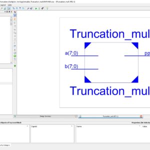
FPGA Implementation of 8×8 Truncated Multiplier
Proposed Abstract:
The operation of multiplication is an often encountered need in the field of digital signal processing. Parallel multipliers provide a rapid approach for performing multiplication operations, while demanding a significant amount of space in VLSI (Very Large Scale Integration) implementations. In the majority of signal processing applications, there is a preference for using a rounded result in order to prevent an increase in the size of the word. Therefore, an important goal in the design process is to minimize the spatial demand of the rounded output multiplier. This study introduces a novel approach to parallel multiplication that efficiently calculates the products of two n-bit values by selectively summing the most important columns using a variable correction technique. This research furthermore includes a comparative analysis of the implementation of 8X8 conventional and truncated multipliers using Verilog Hardware Description Language (HDL) on Field Programmable Gate Arrays (FPGAs). The shortened multiplier demonstrates a much greater decrease in device consumption as compared to the regular multiplier. A conventional multiplier performs computations on n x n bits and produces a weighted sum of the output, consisting of 2n bits. In contrast, a truncated multiplier generates an output of just n bits from the n x n bit input. The use of logic gates in both internal and external hardware design will be decreased. Truncated multipliers provide a viable approach for achieving significant reductions in FPGA resources, latency, and power consumption compared to regular parallel multipliers, particularly in scenarios where the complete accuracy provided by the standard multiplier is unnecessary.
List of the following materials will be included with the Downloaded Backup: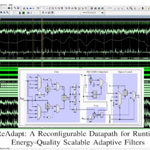
ReAdapt: A Reconfigurable Datapath for Runtime Energy-Quality Scalable Adaptive Filters
Base Paper Abstract:
This paper proposes ReAdapt–a reconfigurable datapath architecture for scaling the energy-quality trade-off of adaptive filtering at runtime. The ReAdapt can dynamically select four adaptive filtering algorithms for gradating complexity levels during runtime by reconfiguring the processing flow in its datapath and by blocking the switching activity (e.g., reducing the CMOS dynamic power) of unused modules with data-gating. The ReAdapt proposal can scale the energy-quality trade-off by choosing the following four different levels of filter algorithms complexity: 1) least mean square (LMS); 2) partial update normalized LMS (PU-NLMS); 3) set-membership normalized LMS (SM-NLMS); 4) normalized LMS (NLMS). The ReAdapt architecture reuses common modules of each adaptive filter, resulting in a compact VLSI hardware implementation. The ReAdapt architecture operation is implemented in a case-study for interference mitigation for electroencephalogram (EEG) signal processing. The hardware synthesis results show an increase of 6.80 times in throughput and at least a reduction of 2.84 times in energy per operation compared with the state-of-the-art adaptive filters. This paper also investigates the benefits of dynamically reconfiguring the four ReAdapt operating modes at runtime for different levels of signal-to-noise ratio (SNR) for the processed signals. We also demonstrate that dynamically reconfiguring the ReAdapt operating modes during runtime results in an optimal energy-quality trade-off which is advantageous over the conventional single static mode.
List of the following materials will be included with the Downloaded Backup: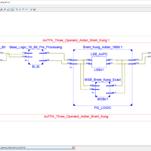
AxPPA: Approximate Parallel Prefix Adders
Base Paper Abstract:
Addition units are widely used in many computational kernels of several error-tolerant applications such as machine learning and signal, image, and video processing. Besides their use as stand-alone, additions are essential building blocks for other math operations such as subtraction, comparison, multiplication, squaring, and division. The parallel prefix adders (PPAs) is among the fastest adders. It represents a parallel prefix graph consisting of the carry operator nodes, called prefix operators (POs). The PPAs, in particular, are among the fastest adders because they optimize the parallelization of the carry generation (G) and propagation (P). In this work, we introduce approximate PPAs (AxPPAs) by exploiting approximations in the POs. To evaluate our proposal for approximate POs (AxPOs), we generate the following AxPPAs, consisting of a set of four PPAs: approximate Brent–Kung (AxPPA-BK), approximate Kogge–Stone (AxPPAKS), Ladner-Fischer (AxPPA-LF), and Sklansky (AxPPA-SK). We compare four AxPPA architectures with energy-efficient approximate adders (AxAs) [i.e., Copy, error-tolerant adder I (ETAI), lower-part OR adder (LOA), and Truncation (trunc)]. We tested them generically in stand-alone cases and embedded them in two important signal processing application kernels: a sum of squared differences (SSDs) video accelerator and a finite impulse response (FIR) filter kernel. The AxPPA-LF provides a new Pareto front in both energy-quality and area-quality results compared to state-of-the-art energy-efficient AxAs.
List of the following materials will be included with the Downloaded Backup:
Design of ultra-low power consumption approximate 4-2 compressors based on the compensation characteristic
Abstract:
Approximate computing is tentatively applied in some digital signal processing applications which have an inherent tolerance for erroneous computing results. The approximate arithmetic blocks are utilized in them to improve the electrical performance of these circuits. Multiplier is one of the fundamental units in computer arithmetic blocks. Moreover, the 4-2 compressors are widely employed in the parallel multipliers to accelerate the compression process of partial products. In this paper, three novel approximate 4-2 compressors are proposed and utilized in 8-bit multipliers. Meanwhile, an error-correcting module (ECM) is presented to promote the error performance of approximate multiplier with the proposed 4-2 compressors. In this paper, the number of the approximate 4-2 compressor’s outputs is innovatively reduced to one, which brings further improvements in the energy efficiency. Compared with the exact 4-2 compressors, the simulation results indicate that the proposed approximate compressors UCAC1, UCAC2, UCAC3 achieve 24.76%, 51.43%, and 66.67% reduction in delay, 71.76%, 83.06%, and 93.28% reduction in power and 54.02%, 79.32%, and 93.10% reduction in area, respectively. And the utilization of these proposed compressors in 8-bit multipliers brings 49.29% reduction of power consumption on average.
List of the following materials will be included with the Downloaded Backup: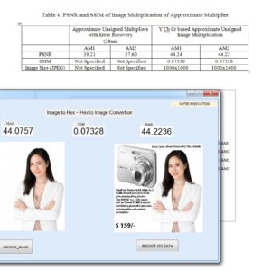
Low-Power Approximate Unsigned Multipliers with Configurable Error Recovery
Abstract:
Approximate circuits have been considered for applications that can tolerate some loss of accuracy with improved performance and/or energy efficiency. Multipliers are key arithmetic circuits in many of these applications including digital signal processing (DSP). In this paper, a novel approximate multiplier with a low power consumption and a short critical path is proposed for high-performance DSP applications. This multiplier leverages a newly designed approximate adder that limits its carry propagation to the nearest neighbors for fast partial product accumulation. Different levels of accuracy can be achieved by using either OR gates or the proposed approximate adder in a configurable error recovery. The multipliers using these two error reduction strategies are referred to as approximate multiplier 1 (AM1) and approximate multiplier 2 (AM2), respectively. Both AM1 and AM2 have a low mean error distance, i.e., most of the errors are not significant in magnitude. Compared to a Wallace multiplier optimized for speed, an 8×8 AM1 with 4 MSBs (most significant bits) for error reduction and synthesized using a 28 nm CMOS process shows a 60% reduction in delay (when optimized for delay) and a 42% reduction in power dissipation (when optimized for area). In a 16×16 design, half of the least significant partial products are truncated for AM1 and AM2, which are thus denoted as TAM1 and TAM2, respectively. Compared with the Wallace multiplier, TAM1 and TAM2 save from 50% to 66% in power, when optimized for area. Compared to existing approximate multipliers, AM1, AM2, TAM1 and TAM2 show significant advantages in accuracy with a high performance. AM2 has a better accuracy compared to AM1 but with a longer delay and higher power consumption. Image processing applications including image sharpening and smoothing are considered to show the quality of the approximate multipliers in error-tolerant applications. By utilizing an appropriate error recovery, the proposed approximate multipliers achieve similar processing accuracy as traditional exact multipliers, but with significant improvements in power.
List of the following materials will be included with the Downloaded Backup:
FIR Filter Design based on FPGA
Abstract:
FIR (Finite Impulse Response) Filters: the finite impulse response filter is the most basic components in digital signal processing systems are widely used in communications, image processing, and pattern recognition. Based on FPGA(editable logic device) to achieve FIR filter, not only take into account the fixed -function DSP-specific chip real-time, but also has the DSP processor flexibility. The combination of FPGA and DSP technology can further improve integration, increase work speed and expand system capabilities.
List of the following materials will be included with the Downloaded Backup:
Approximate Sum-of-Products Design Based on Distributed Arithmetic
Proposed Abstract:
Approximate circuits provide high performance and require low power. Sum-of-products (SOP) units are key elements in many digital signal processing applications. In this brief, three approximate SOP (ASOP) models which are based on the distributed arithmetic are proposed. They are designed for different levels of accuracy. First model of ASOP achieves an improvement up to 64% on area and 70% on power, when compared with conventional unit. Other two models provide an improvement of 32% and 48% on area and 54% and 58% on power, respectively, with a reduced error rate compared with the first model. Third model achieves the mean relative error and normalized error distance as low as 0.05% and 0.009%, respectively. Performance of approximate units is evaluated with a noisy image smoothing application, where the proposed models are capable of achieving higher peak signal to-noise ratio than the existing state-of-the-art techniques. It is shown that the proposed approximate models achieve higher processing accuracy than existing works but with significant improvements in power and performance.
List of the following materials will be included with the Downloaded Backup:
Input Based Dynamic Reconfiguration of Approximate Arithmetic Units for Video Encoding
Abstract:
The field of approximate computing has receivedsignificant attention from the research community in the pastfew years, especially in the context of various signal processingapplications. Image and video compression algorithms, such asJPEG, MPEG, and so on, are particularly attractive candidatesfor approximate computing, since they are tolerant of computingimprecision due to human imperceptibility, which can beexploited to realize highly power-efficient implementations ofthese algorithms. However, existing approximate architecturestypically fix the level of hardware approximation staticallyand are not adaptive to input data. For example, if afixed approximate hardware configuration is used for anMPEG encoder (i.e., a fixed level of approximation), theoutput quality varies greatly for different input videos. Thispaper addresses this issue by proposing a reconfigurableapproximate architecture for MPEG encoders thatoptimizespower consumption with the goal of maintaining a particularPeak Signal-to-Noise Ratio (PSNR) threshold for any video.We propose two heuristics for automaticallytuning the approximation degree of the RABs in thesetwo modules during runtime based on the characteristics of eachindividual video. The proposed architecture of this paper analysis the logic size, area and power consumption using Xilinx 14.2.
List of the following materials will be included with the Downloaded Backup:
Obfuscating DSP Circuits via High Level Transformations
This paper presents a novel approach to design obfuscated circuits for digital signal processing (DSP) applications using high-level transformations, a key-based obfuscating finite-state machine (FSM), and a reconfigurator. The goal is to design DSP circuits that are harder to reverse engineer. High level transformations of iterative data-flow graphs have been exploited for area-speed-power tradeoffs. This is the first attempt to develop a design flow to apply high level transformations that not only meet these tradeoffs but also simultaneously obfuscate the architectures both structurally and functionally. Functional obfuscation is accomplished by requiring use of the correct initialization key, and configure data. Structural obfuscation is also achieved by the proposed methodology via high-level transformations. The proposed architecture of this paper analysis the logic size, area and power consumption using Xilinx 14.2
List of the following materials will be included with the Downloaded Backup:
Design and Analysis of a Majority Logic Based Imprecise 6-2 Compressor for Approximate Multipliers
Base Paper Abstract:
Approximate computing is an emerging paradigm for trading off computing accuracy to reduce energy consumption and design complexity in a variety of applications, for which exact computation is not a critical requirement. Different from conventional designs using AND-OR and XOR gates, the majority gate is widely used in many emerging nanotechnologies. An ultra-efficient 6-2 compressor is proposed in this paper. It is composed of two majority gates that lead to low energy consumption and high hardware efficiency. The proposed compressor is utilized in the approximate partial product reduction of a modified 8×8 Dadda multiplier with a truncated structure. Experimental results show that this multiplier realizes a significant reduction in hardware cost, especially in terms of power and area, on average by up to 40% and 31% respectively, compared to exact and state-of-the-art designs. The application of image multiplication is also presented to assess the practicability of the multiplier. The results show that the proposed multiplier results in images with higher quality in peak signal to noise ratio (PSNR) and mean structural similarity index metric (MSSIM) compared to other designs.
List of the following materials will be included with the Downloaded Backup:
Fast and Hardware-Efficient Variable Step Size Adaptive Beamformer
Base Paper Abstract:
Constant step size least mean square (CSS-LMS) is one of the most popular adaptive beamforming algorithms. However, for varying channel signal-to-noise ratios (SNRs), the CSS algorithms are not effective, and there is a need for variable step size (VSS) algorithms. The VSS algorithms provide extremely deep nulls for the interferences; however, they are complex to implement on hardware. Hence, this paper proposes two hardware-efficient variable step size algorithms, namely, efficient variable step size LMS (EVSS-LMS) and reduced complexity parallel LMS (EVSS-RC-pLMS). The proposed EVSS algorithms eliminate the complex operations of VSS algorithms like division and exponential and approximate them to simpler operations. Further, MATLAB simulations demonstrate accelerated convergence, deep nulls, a lower error floor, and better performance in varying SNR environments for the proposed algorithms. Additionally, the finite precision radiation patterns are similar to infinite precision. Hardware synthesis results show the outstanding performance of EVSS in terms of resource utilization on the Xilinx Artix-7 FPGA.
List of the following materials will be included with the Downloaded Backup:
An Optimization in Conventional Shift &Add Multiplier for Area-Efficient Implementation on FPGA
Base Paper Abstract:
FPGA is familiar with prototyping and implementing simple to complex DSP systems. The FPGA based design may be highly affected by factors that include selection of an FPGA board, Electronic Design Automation Tool and the Programming Techniques to optimize the algorithm. The algorithm optimization results in a more compact design regarding the area and achieved frequency. In DSP algorithms optimization, the major bottleneck is the multiplier complexity evident in, for example - FIR, IIR, FFT, and others. Research shows much work on multiplier optimization. Despite all possible optimization techniques, the multiplier consumes tremendous resources when translated on hardware, with more power consumption and observed delay. The proposed work is novel in that it brings resources optimization in a familiar shift and add multiplier algorithm by implementing the design in FPGA and comparing the results with the existing shift, and add a multiplier. In the implementation of the design, Xilinx Vertex -7 FPGA is used along with ISE 14.2 simulators. The parameters to compare are the Lookup tables (Logic element of FPGA), adder/subtractors and the multiplexers, along with performance characters, like the operating frequency, delay and total levels of logic (path travelled by the signal in register transfer level). The output shows that the anticipated design is an excellent alternative to the conventional shift and add algorithm.
List of the following materials will be included with the Downloaded Backup: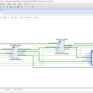
FPGA Implementation of D8PSK Demodulator
Base Paper Abstract:
Differential phase shift keying (DPSK) is a modulation scheme that facilitates non coherent demodulation and is employed for various applications such as Wireless Local Area Networks (WLANs), Bluetooth and RFID communication. In this paper, design, development and hardware implementation of a new demapping scheme for Differential 8-PSK (D8PSK) demodulator on a Zynq 7000 FPGA based ZED board is proposed using the concepts of model based design. The proposed work can be easily extended to other M-ary DPSK schemes.
List of the following materials will be included with the Downloaded Backup:
A Low Power and High Speed Voltage Level Shifter Based on a Regulated Cross Coupled Pull Up Network
Abstract:
In this brief, a fast and very low power voltage level shifter (LS) is presented. By using a new regulated cross-coupled (RCC) pull-up network, the switching speed is boosted and the dynamic power consumption is highly reduced. The proposed (LS) has the ability to convert input signals with voltage levels much lower than the threshold voltage of a MOS device to higher nominal supply voltage levels. The presented LS occupies a small silicon area owing to its very low number of elements and is ultra-low-power, making it suitable for low-power applications such as implantable medical devices and wireless sensor networks. Results of the post-layout simulation in a standard 0.18-μm CMOS technology show that the proposed circuit can convert up input voltage levels as low as 80 mV. The power dissipation and propagation delay of the proposed level shifter for a low/high supply voltages of 0.4/1.8 V and input frequency of 1 MHz are 123.1 nW and 23.7 ns, respectively.
List of the following materials will be included with the Downloaded Backup:
Feed forward-Cutset-Free Pipelined Multiply–Accumulate Unit for the Machine Learning Accelerator
Abstract:
Multiply–accumulate (MAC) computations account for a large part of machine learning accelerator operations. The pipelined structure is usually adopted to improve the performance by reducing the length of critical paths. An increase in the number of flip-flops due to pipelining, however, generally results in significant area and power increase. A large number of flip-flops are often required to meet the feed forward-cutset rule. Based on the observation that this rule can be relaxed in machine learning applications, we propose a pipelining method that eliminates some of the flip-flops selectively. The simulation results show that the proposed MAC unit achieved a 20% energy saving and a 20% area reduction compared with the conventional pipelined MAC.
List of the following materials will be included with the Downloaded Backup:
A Two-Speed, Radix-4, Serial–Parallel Multiplier (Booth Multiplier )
Abstract:
In this paper, we present a two-speed, radix-4, serial-parallel multiplier for accelerating applications such as digital filters, artificial neural networks, and other machine learning algorithms. Our multiplier is a variant of the serial–parallel (SP) modified radix-4 Booth multiplier that adds only the nonzero Booth encodings and skips over the zero operations, making the latency dependent on the multiplier value. Two sub circuits with different critical paths are utilized so that throughput and latency are improved for a subset of multiplier values. The multiplier is evaluated on an Intel Cyclone V field-programmable gate array against standard parallel–parallel and SP multipliers across four different process–voltage–temperature corners. We show that for bit widths of 32 and 64, our optimizations can result in a 1.42×–3.36× improvement over the standard parallel Booth multiplier in terms of area–time depending on the input set.
List of the following materials will be included with the Downloaded Backup:
Area-Efficient Bidirectional Shift-Register Using Bidirectional Pulsed-Latches
Abstract:
This paper proposes an area-efficient bidirectional shift-register using bidirectional pulsed-latches. The proposed bidirectional shift-register reduces the area and power consumption by replacing master-slave flip-flops and 2-to-1 multiplexers with the proposed bidirectional pulsed-latches and non-overlap delayed pulsed clock signals, and by using sub shift-registers and extra temporary storage latches. A 256-bit bidirectional shift-register was fabricated using a 65nm CMOS process. Its area was 1,943μm2 and its power consumption is 200μW at a 100MHz clock frequency with VDD=1.2V. It reduces area by 39.2% and power consumption by 19.4% compared to the conventional bidirectional shift-register, length in most cases.
List of the following materials will be included with the Downloaded Backup:
Highly Linear Low-Power Wireless RF Receiver for WSN
Abstract:
This paper introduces a low-power wireless RF receiver for the wireless sensor network. The receiver has improved linearity with incorporated current-mode circuits and high-selectivity filtering. The receiver operates at the 900-MHz industrial, scientific, and medical band and is implemented in 130-nm CMOS technology. The receiver has a frequency multiplication mixer, which uses a 300-MHz clock from a local oscillator (LO). The LO is implemented using vertical delay cells to reduce power consumption. The receiver conversion gain is 40 dB and the receiver noise. The receiver’s input third-order intercept point (IIP3) is −6 dBm and the total power consumption is 1.16 mW.
List of the following materials will be included with the Downloaded Backup:
Design of Sparse FIR Filters With Reduced Effective Length
Abstract:
In this paper, an exchange algorithm is proposed to design sparse linear phase finite impulse response (FIR) filters with reduced effective length. The sparse FIR filter design problem is formally an l0-norm minimization problem. This original design problem is re-formulated by encoding the filter coefficients using a binary encoding vector, which represents the locations of the zero and non-zero filter coefficients. An iterative 0-1 exchange process with proper direction control is proposed to propel the minimax approximation error toward the specified upper bound of error for sparsity maximization. The effective length is optimized with a lower priority than sparsity in the proposed algorithm. Simulation results show that the proposed algorithm is superior to the existing algorithms in terms of both sparsity and/or effective length in most cases.
List of the following materials will be included with the Downloaded Backup:
Energy-Quality Scalable Adders Based on Non-zeroing Bit Truncation
Abstract:
Approximate addition is a technique to trade off energy consumption and output quality in error-tolerant applications. In prior art, bit truncation has been explored as a lever to dynamically trade off energy and quality. In this brief, an innovative bit truncation strategy is proposed to achieve more graceful quality degradation compared to state-of-the-art truncation schemes. This translates into energy reduction at a given quality target. When applied to a ripple-carry adder, the proposed bit truncation approach improves quality by up to 8.5 dB in terms of peak signal-to-noise ratio, compared to traditional bit truncation. As a case study, the proposed approach was applied to a discrete cosine transform engine. In comparison with prior art, the proposed approach reduces energy by 20%, at insignificant delay and silicon area overhead.
List of the following materials will be included with the Downloaded Backup:
World’s Fastest FFT Architectures: Breaking the Barrier of 100 GS/s
Abstract:
This paper presents the fastest fast Fourier transform (FFT) hardware architectures so far. The architectures are based on a fully parallel implementation of the FFT algorithm. In order to obtain the highest throughput while keeping the resource utilization low, we base our design on making use of advanced shift-and-add techniques to implement the rotators and on selecting the most suitable FFT algorithms for these architectures. Apart from high throughput and resource efficiency, we also guarantee high accuracy in the proposed architectures. For the implementation, we have developed an automatic tool that generates the architectures as a function of the FFT size, input word length and accuracy of the rotations. We provide experimental results covering various FFT sizes, FFT algorithms, and field-programmable gate array boards. These results show that it is possible to break the barrier of 100 GS/s for FFT calculation.
List of the following materials will be included with the Downloaded Backup:
Analysis, Comparison, and Experimental Validation of a Class AB Voltage Follower With Enhanced Bandwidth and Slew Rate
Abstract:
This paper describes a bandwidth (BW)- and slew rate (SR)-enhanced class AB voltage follower (VF). A thorough small signal analysis of the proposed and a state-of-the-art AB-enhanced VF is presented to compare their performance. The proposed circuit has 50-MHz BW, 19.5-V/µs SR, and a BW figure of merit of 41.6 (MHz × pF/µW) for CL = 50 pF. It provides 13 times higher current efficiency and 15 times higher BW than the conventional VF with equal 60-µW static power dissipation. The experimental and simulation results of a fabricated test chip in the 130-nm CMOS technology validate the proposed circuit.
List of the following materials will be included with the Downloaded Backup:
A 16-bit 2.0-ps Resolution Two-Step TDC in 0.18-μm CMOS Utilizing Pulse-Shrinking Fine Stage
Abstract:
This paper proposes a time-to-digital converter (TDC) that achieves wide input range and fine time resolution at the same time. The proposed TDC utilizes pulse-shrinking (PS) scheme in the second stage for a fine resolution and two-step (TS) architecture for a wide range. The proposed PS TDC prevents an undesirable non-uniform shrinking rate issue in the conventional PS TDCs by utilizing a built-in offset pulse and an offset pulse width detection schemes. With several techniques, including a built-in coarse gain calibration mechanism, the proposed TS architecture overcomes a nonlinearity due to the signal propagation and gain mismatch between coarse and fine stages. The simulation results of the TDC implemented in a 0.18-µm standard CMOS technology demonstrate 2.0-ps resolution and 16-bit range that corresponds to ∼130-ns input time interval with 0.08-mm2 area. It operates at 3.3 MS/s with 18.0 mW from 1.8-V supply and achieves 1.44-ps single-shot precision. Index Terms— Built-in calibration, pulse shrinking (PS), time-to-digital conversion, two step (TS).
List of the following materials will be included with the Downloaded Backup:
Low-Complexity 2-D Digital FIR Filters Using Polyphase Decomposition and Farrow Structure
Abstract:
This paper proposes a novel realization technique for quadrantally symmetric 2-D finite impulse response filters with a guaranteed reduction in the hardware complexity. Here, the concept of Farrow structure-based interpolation filter design using the polyphase decomposition of the 1-D filter transfer function is effectively utilized in the 2-D domain. The proposed 2-D filter makes use of row-wise polyphase decomposition of the 2-D transfer function or frequency response, followed by the polynomial approximation of the individual polyphase coefficients resulting in Farrow structures corresponding to each row filter. The final coefficients are implemented by varying the delay values in all the Farrow structures, followed by the interpolation of the coefficients obtained from each delay value, which in turn forms the rows in the 2-D kernel. The major highlight of the proposed method is the highly reduced implementation complexity in terms of the number of multipliers and adders, with a low normalized root-mean-square error. Design examples of the circularly symmetric and fan-type filters have been considered to show the efficiency of the approach. The results show a drastic reduction in the implementation complexity of the 2-D filters of upto 20%, with significantly low normalized root-mean-square error lesser than 0.5%.
List of the following materials will be included with the Downloaded Backup:
A Low Complexity I/Q Imbalance Calibration Method for Quadrature Modulator
Abstract:
This brief presents a low-complexity I/Q (in-phase and quadrature components) imbalance calibration method for the transmitter using quadrature modulation. Impairments in analog quadrature modulator have a deleterious effect on the signal fidelity. Among the critical impairments, I/Q imbalance (gain and phase mismatches) deteriorates the residual sideband performance of the analog quadrature modulator degrading the error vector magnitude. Based on the theoretical mismatch analysis of the quadrature modulator, we propose a low-complexity I/Q imbalance extraction algorithm. After the parameter extraction, the transmitter is calibrated by imposing the counter imbalanced mismatch of the transmitter through the digital baseband. In comparison with existing I/Q imbalance calibration methods, the novelty of the proposed method lies in that: 1) only three spectrum measurements of the device-under-test are needed for extraction and calibration of gain and phase mismatches; 2) due to the blind nature of the calibration algorithm, the proposed approach can be readily applicable to an existing I/Q transmitter; 3) no extra hardware that degrades the calibration accuracy is required; and 4) due to the non-iterative nature, the proposed method is faster and computationally more efficient than previously published methods.
List of the following materials will be included with the Downloaded Backup:
Low Power and High Speed Implementation of FIR filter design using CMOS GDI Truncated Multiplier
Abstract:
The logic size, propagation delay, power of applications, based upon this improvement the adder design logic size will reduced year by year, here a proposed In recent technology of any application, adders is a more priority to do a function and task of arithmetic operation, in crucial this adder based arithmetic operation will decide work of this paper will design using a single bit full adder to design a multiplier. In this multiplier design, adder is a main priority to reduce the arithmetic logic size and increases speed of multiplier, in recent we have lots of multiplier design, Vedic multiplier, Wallace tree multiplier, booth multiplier, approximate multiplier. Here, the proposed work will taken truncated multiplier design, it's because, the truncated multiplier will have a capability to reduced internal and external architecture size in every design, regarding this truncated multiplier will have three options such as rounding, deleting, truncating, here the MSB bits will be truncated and present the output of n x n multiplication will provided only n bit level, using this truncated multiplier the proposed work will designed a 8-Tap FIR(Finite impulse response) filter and shown the efficiency of filter design using this CMOS GDI (Gate Diffusion Input) adder design. This proposed work will design in CMOS Logic gate and which 10-T transistor level of full adders with 90um technology, finally proved the terms of area, delay and power.
List of the following materials will be included with the Downloaded Backup:
Improving Error Correction Codes for Multiple-Cell Upsets in Space Applications
Proposed Abstract:
Currently, faults suffered by SRAM memory systems have increased due to the aggressive CMOS integration density. Thus, the probability of occurrence of single-cell upsets (SCUs) or multiple-cell upsets (MCUs) augments. One of the main causes of MCUs in space applications is cosmic radiation. A common solution is the use of error correction codes (ECCs). Nevertheless, when using ECCs in space applications, they must achieve a good balance between error coverage and redundancy, and their encoding/decoding circuits must be efficient in terms of area, power, and delay. Different codes have been proposed to tolerate MCUs. For instance, Matrix codes use Hamming codes and parity checks in a bi-dimensional layout to correct and detect some patterns of MCUs. Recently presented, column–line–code (CLC) has been designed to tolerate MCUs in space applications. CLC is a modified Matrix code, based on extended Hamming codes and parity checks. Nevertheless, a common property of these codes is the high redundancy introduced. In this paper, we present a series of new low redundant ECCs able to correct MCUs with reduced area, power, and delay overheads. Also, these new codes maintain, or even improve, memory error coverage with respect to Matrix and CLC codes.
List of the following materials will be included with the Downloaded Backup:
Low-Complexity VLSI Design of Large Integer Multipliers for Fully Homomorphic Encryption
Abstract:
Large integer multiplication has been widely used in fully homomorphic encryption (FHE). Implementing feasible large integer multiplication hardware is thus critical for accelerating the FHE evaluation process. In this paper, a novel and efficient operand reduction scheme is proposed to reduce the area requirement of radix-r butterfly units. We also extend the single port, merged-bank memory structure to the design of number theoretic transform (NTT) and inverse NTT (INTT) for further area minimization. In addition, an efficient memory addressing scheme is developed to support both NTT/INTT and resolving carries computations. Experimental results reveal that significant area reductions can be achieved for the targeted 786 432- and 1 179 648-bit NTT-based multipliers designed using the proposed schemes in comparison with the related works. Moreover, the two multiplications can be accomplished in 0.196 and 2.21 ms, respectively, based on 90-nm CMOS technology. The low-complexity feature of the proposed large integer multiplier designs is thus obtained without sacrificing the time performance.
List of the following materials will be included with the Downloaded Backup:
Design and Low-Complexity Implementation of Matrix–Vector Multiplier for Iterative Methods in Communication Systems
Abstract: Iterative methods are basic building blocks of communication systems and often represent a dominating part of the system, and therefore, they necessitate careful design and implementation for optimal performance. In this brief, we propose a novel field programmable gate arrays design of matrix–vector multiplier that can be used to efficiently implement widely adopted iterative methods. The proposed design exploits the sparse structure of the matrix as well as the fact that spreading code matrices have equal magnitude entries. Implementation details and timing analysis results are promising and are shown to satisfy most modern communication system requirements.
List of the following materials will be included with the Downloaded Backup:
MInSC: A VLSI Architecture for Myocardial Infarction Stages Classifier for Wearable Healthcare Applications
Base Paper Abstract:
Myocardial Infarction (MI) is a critical heart abnormality causing millions of fatalities worldwide every year. MI progress in three stages based on its severity causing several changes in an Electrocardiogram (ECG) signal. It is very critical to capture these variations, which requires continuous monitoring of the ECG signal of the patient. Therefore, it becomes imperative to develop a low power VLSI architecture to address the prognosis of MI. In this brief, for the first time, an area and power efficient design of a five stage classifier is proposed, which detects the progression of various stages of MI using ECG beats in real time. The proposed architecture has an area and total power utilization of 1.38mm2 and 5.12µW, respectively at SCL 180nm Bulk CMOS technology. The low power and area requirements and multiclass classification capability of the proposed design make it suitable to be used in wearable devices.
List of the following materials will be included with the Downloaded Backup:
FPGA Implementation of Image Line Buffer to Split and reconstruct a 3×3 size of image pixel with using FIFO Design
Proposed Abstract:
Image line buffers are used in several kinds of image processing applications, particularly where operations must be executed on a per-line basis in order to optimize efficiency. There are many typical applications associated with this technology, including real-time video processing, image filtering, edge detection, computer vision, memory optimization, parallel processing, compression algorithms, and medical imaging. In the context of image and video processing applications, the use of image line buffers may contribute to the optimization of operations when dealing with a continuous stream of frames processed in real time. In the context of image processing, convolutional processes are often used for tasks like as image filtering and blurring. These operations are typically carried out on a per-pixel basis, wherein the value assigned to each pixel is determined by the values of its adjacent pixels. The proposed structure was created using a First-In-First-Out (FIFO) based approach, aiming to decrease the number of logic sizes and complexity in Very Large Scale Integration (VLSI) design architecture. The conversion of design images to hexadecimal and hexadecimal to image format is accomplished using MATLAB GUI applications. These applications also facilitate the comparison of Peak Signal-to-Noise Ratio (PSNR) and Structural Similarity Index Measure (SSIM) values. The internal architecture of the system is implemented using Verilog Hardware Description Language (HDL). Additionally, the simulation is conducted using Modelsim. Furthermore, the system's performance parameters, including area, delay, and power consumption, are compared with those of the Xilinx Vertex-5 Field Programmable Gate Array (FPGA).
List of the following materials will be included with the Downloaded Backup:
Hamming based Single Fault Error Correction Code
Proposed Abstract:
Signal processing and communication systems often use digital filters. In certain circumstances, the dependability of such systems is essential, prompting the construction of fault-tolerant filters. Many methods that take use of the structure and characteristics of the filters to achieve fault tolerance have been put forward throughout the years. Technology advances permit more intricate systems with several filters. It is typical for some of the filters in such complicated systems to function in simultaneously, for instance by using the same filter on several input signals. Recently, a straightforward method for achieving fault tolerance was given that takes use of the existence of parallel filters. This paper expands on that concept to demonstrate how error correction codes (ECCs), in which each filter is the equivalent of a bit in a conventional ECC, may be used to secure parallel filters. When there are several parallel filters operating simultaneously, this new technique enables more effective protection. The efficiency of the method in terms of protection and implementation cost is assessed using a case study of parallel finite impulse response filters.
List of the following materials will be included with the Downloaded Backup:
Design of SEU Tolerant 2D-FFT in SRAM-based FPGA
Base Paper Abstract:
2-Dimensional fast Fourier transform (FFT) has been widely used in radar signal process. Due to the need for high performance, field programmable gate array (FPGA) is an ideal hardware device for this application. For space-borne radar platform such as synthetic aperture radar (SAR), single-event upsets (SEUs) can cause lots of soft errors in static random access memory (SRAM) based FPGA. As to this, protecting the 2D-FFT implemented in FPGA from SEUs is very important. In this article, we analyze the critical weakness induced by SEUs in the 2D-FFT process, and then a 2D-FFT design with high SEU resilience is presented. The design utilizes the advantage of several anti-SEU methods. For butterfly control in FFT, partially triple modular redundancy (TMR) is used. For data buffers, error correction code (ECC) is applied to read and write operation. Furthermore, safe finite state machine (FSM) is adopted by important control registers. Fault injection results show that all these reinforcement technologies contribute to enhance the ability to mitigate the SEU effects.
List of the following materials will be included with the Downloaded Backup:
A High-Speed FPGA-based True Random Number Generator using Metastability with Clock Managers
Base Paper Abstract:
True random number generators (TRNGs) are fundamentals in many important security applications. Though they exploit randomness sources that are typical of the analog domain, digital-based solutions are strongly required especially when they have to be implemented on Field Programmable Gate Array (FPGA)-based digital systems. This paper describes a novel methodology to easily design a TRNG on FPGA devices. It exploits the runtime capability of the Digital Clock Manager (DCM) hardware primitives to tune the phase shift between two clock signals. The presented auto-tuning strategy automatically sets the phase difference of two clock signals in order to force on one or more flip-flops (FFs) to enter the metastability region, used as a randomness source. Moreover, a novel use of the fast carry-chain hardware primitive is proposed to further increase the randomness of the generated bits. Finally, an effective on-chip post-processing scheme that does not reduce the TRNG throughput is described. The proposed TRNG architecture has been implemented on the Xilinx Zynq XC7Z020 System on Chip (SoC). It passed all the National Institute of Standards and Technology (NIST) SP 800-22 statistical tests with a maximum throughput of 300×106 bit per second. The latter is considerably higher than the throughput of other previously published DCMbased TRNGs.
List of the following materials will be included with the Downloaded Backup:
Area Delay and Energy Efficient Multi-Operand Binary Tree Adder
Abstract:
Here, the critical path of ripple carry adder (RCA)-based binary tree adder (BTA) is analyzed to find the possibilities for delay minimization. Based on the findings of the analysis, the new logic formulation and the corresponding design of RCA are proposed for the BTA. The comparison result shows that the proposed RCA design offers better efficiency in terms of area, delay and energy than the existing RCA. Using this RCA design, the BTA structure is proposed. The synthesis result reveals that the proposed 32-operand BTA provides the saving of 22.5% in area–delay product and 28.7% in energy–delay product over the recent Wallace tree adder which is the best among available multi-operand adders. The authors have also applied the proposed BTA in the recent multiplier designs to evaluate its performance. The synthesis result shows that the performance of multiplier designs improved significantly due to the use of proposed BTA. Therefore, the proposed BTA design can be a better choice to develop the area, delay and energy efficient digital systems for signal and image processing applications.
List of the following materials will be included with the Downloaded Backup:
Energy-Efficient Approximate Multiplier Design using Bit Significance-Driven Logic Compression
Abstract:
Approximate arithmetic has recently emerged as a promising paradigm for many imprecision-tolerant applications. It can offer substantial reductions in circuit complexity, delay and energy consumption by relaxing accuracy requirements. In this paper, we propose a novel energy-efficient approximate multiplier design using a significance-driven logic compression (SDLC) approach. Fundamental to this approach is an algorithmic and configurable lossy compression of the partial product rows based on their progressive bit significance. This is followed by the commutative remapping of the resulting product terms to reduce the number of product rows. As such, the complexity of the multiplier in terms of logic cell counts and lengths of critical paths is drastically reduced. A number of multipliers with different bit-widths (4-bit to 128-bit) are designed in System Verilog and synthesized using Synopsys Design Compiler. Post-synthesis experiments showed that up to an order of magnitude energy savings, and reductions of 65% in critical delay and almost 45% in silicon area can be achieved for a 128-bit multiplier compared to an accurate equivalent. These gains are achieved with low accuracy losses estimated at less than 0.00071 mean relative error. Additionally, we demonstrate the energy-accuracy trade-offs for different degrees of compression, achieved through configurable logic clustering. In evaluating the effectiveness of our approach, a case study image processing application showed up to 68.3% energy reduction with negligible losses in image quality expressed as peak signal-to-noise ratio (PSNR).
List of the following materials will be included with the Downloaded Backup: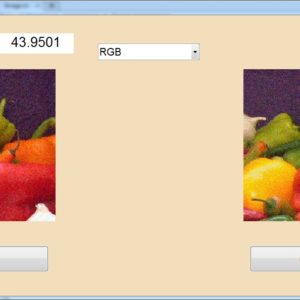
Design of Power and Area Efficient Approximate Multipliers
Abstract:
Approximate computing can decrease the design complexity with an increase in performance and power efficiency for error resilient applications. This brief deals with a new design approach for approximation of multipliers. The partial products of the multiplier are altered to introduce varying probability terms. Logic complexity of approximation is varied for the accumulation of altered partial products based on their probability. The proposed approximation is utilized in two variants of 16-bit multipliers. Synthesis results reveal that two proposed multipliers achieve power savings of 72% and 38%, respectively, compared to an exact multiplier. They have better precision when compared to existing approximate multipliers. Mean relative error figures are as low as 7.6% and 0.02% for the proposed approximate multipliers, which are better than the previous works. Performance of the proposed multipliers is evaluated with an image processing application, where one of the proposed models achieves the highest peak signal to noise ratio.
List of the following materials will be included with the Downloaded Backup:
Low Power Split Radix FFT Processors Using Radix 2 Butterfly Units
Split radix fast Fourier Transform (SRFFT) is an ideal candidate for the implementation of a low power FFT processor, because it has the lowest number of arithmetic operation among all the FFT algorithms. In the design of such processors, an efficient addressing scheme for FFT data as well as twiddle factors is required. The signal flow graph of SRFFT is the same as radix-2 FFT, and therefore, the conventional address generation schemes of FFT data could also be applied to SRFFT. However SRFFT has irregular locations of twiddle factors and forbids the application of radix-2 address generation methods. This brief presents a shared memory low power SRFFT processor architecture. The SRFFT can be computed by using a modified radix-2 butterfly unit. The butterfly unit exploits the multiplier-gating technique to save dynamic power at the expense of using more hardware resources. In addition, two novel address generation algorithm for both the trivial and nontrivial twiddle factors are developed. In this paper We increases the architecture size, of radix-4 and 2048 point complex valued transform, and shown the performance of area, power and delay, and synthesized xilinx FPGA on s6lx16-2csg225.
List of the following materials will be included with the Downloaded Backup:
RF Power Gating A Low Power Technique for Adaptive Radios
Low Power FPGA Design Using Memoization Based Approximate Computing
Field-programmable gate arrays (FPGAs) are increasingly used as the computing platform for fast and energy efficient execution of recognition, mining, and search applications. Approximate computing is one promising method for achieving energy efficiency. Compared with most prior works on approximate computing, which target approximate processors and arithmetic blocks, this paper presents an approximate computing methodology for FPGA-based design. It studies memoization as a method for approximation on FPGA and analyzes different architectural and design parameters that should be considered. The proposed design flow leverages on high-level synthesis to enable memoization-based microarchitecture generation, thus also facilitating a C-to-register-transfer-level synthesis. When compared with the previous approaches of bit-width truncation and approximate multipliers, memoization-based approximate computation on FPGA achieves a significant dynamic power saving (around 20%) with very small area overhead (<5%) and better power-to-signal noise ratio values for the studied image processing benchmarks. The proposed architecture of this paper is verified using vivado HLS..
List of the following materials will be included with the Downloaded Backup:
A Computation and Energy Reduction Technique for HEVC Discrete Cosine Transform
In this paper, a novel computation and energy reduction technique for High Efficiency Video Coding (HEVC) Discrete Cosine Transform (DCT) for all Transform Unit (TU) sizes is proposed. The proposed technique reduces the computational complexity of HEVC DCT significantly at the expense of slight decrease in PSNR and slight increase in bit rate by only calculating several pre-determined low frequency coefficients of TUs and assuming that the remaining coefficients are zero. It reduced the execution time of HEVC HM software encoder up to 12.74%, and it reduced the execution time of DCT operations in HEVC HM software encoder up to 37.27%. In this paper, a low energy HEVC 2D DCT hardware for all TU sizes is also designed and implemented using Verilog HDL. The proposed hardware, in the worst case, can process 53 Ultra HD (7680x4320) video frames per second. The proposed technique reduced the energy consumption of this hardware up to 18.9%. Therefore, it can be used in portable consumer electronics products that require a real-time HEVC encoder. The proposed architecture of this paper analysis the logic size, area and power consumption using Xilinx 14.2.
List of the following materials will be included with the Downloaded Backup:Provide Wordlwide Online Support
We can provide Online Support Wordlwide, with proper execution, explanation and additionally provide explanation video file for execution and explanations.
24/7 Support Center
NXFEE, will Provide on 24x7 Online Support, You can call or text at +91 9789443203, or email us nxfee.innovation@gmail.com
Terms & Conditions:
Customer are advice to watch the project video file output, and before the payment to test the requirement, correction will be applicable.
After payment, if any correction in the Project is accepted, but requirement changes is applicable with updated charges based upon the requirement.
After payment the student having doubts, correction, software error, hardware errors, coding doubts are accepted.
Online support will not be given more than 3 times.
On first time explanation we can provide completely with video file support, other 2 we can provide doubt clarifications only.
If any Issue on Software license / System Error we can support and rectify that within end of day.
Extra Charges For duplicate bill copy. Bill must be paid in full, No part payment will be accepted.
After payment, to must send the payment receipt to our email id.
Powered by NXFEE INNOVATION, Pondicherry.
Call us today at : +91 9789443203 or Email us at nxfee.innovation@gmail.com
NXFEE Development & Services

Product Categories
- 2014 (12)
- 2015 (39)
- 2016 (31)
- 2017 (16)
- 2018 (17)
- 2019 (42)
- 2020 (29)
- 2021 (16)
- 2022 (22)
- 2023 (17)
- Area Efficient (92)
- High speed VLSI Design (49)
- IEEE (16)
- Image Processing (34)
- Low power VLSI Design (71)
- NOC VLSI Design (3)
- VLSI (180)
- VLSI Application / Interface and Mini Projects (13)
- VLSI_2023 (15)
Filter by price
Product Status
Sort by producents

Copyright © 2021 Nxfee Innovation.