MInSC: A VLSI Architecture for Myocardial Infarction Stages Classifier for Wearable Healthcare Applications
Base Paper Abstract:
Myocardial Infarction (MI) is a critical heart abnormality causing millions of fatalities worldwide every year. MI progress in three stages based on its severity causing several changes in an Electrocardiogram (ECG) signal. It is very critical to capture these variations, which requires continuous monitoring of the ECG signal of the patient. Therefore, it becomes imperative to develop a low power VLSI architecture to address the prognosis of MI. In this brief, for the first time, an area and power efficient design of a five stage classifier is proposed, which detects the progression of various stages of MI using ECG beats in real time. The proposed architecture has an area and total power utilization of 1.38mm2 and 5.12µW, respectively at SCL 180nm Bulk CMOS technology. The low power and area requirements and multiclass classification capability of the proposed design make it suitable to be used in wearable devices.
List of the following materials will be included with the Downloaded Backup:
Modified Wallace Tree Multiplier using Efficient Square Root Carry Select Adder
A multiplier is one of the key hardware blocks in most digital and high performance systems such as FIR filters, micro processors and digital signal processors etc. A system’s performance is generally determined by the performance of the multiplier because the multiplier is generally the slowest element in the whole system and also it is occupying more area consuming. The Carry Select Adder (CSLA) provides a good compromise between cost and performance in carry propagation adder design. A Square Root Carry Select Adder using RCA is introduced but it offers some speed penalty. However, conventional CSLA is still area-consuming due to the dual ripple carry adder structure. In the proposed work, generally in Wallace multiplier the partial products are reduced as soon as possible and the final carry propagation path carry select adder is used. In this paper, modification is done at gate level to reduce area and power consumption. The Modified Square Root Carry Select-Adder (MCSLA) is designed using Common Boolean Logic and then compared with regular CSLA respective architectures, and this MCSLA is implemented in Wallace Tree Multiplier. This work gives the reduced area compared to normal Wallace tree multiplier. Finally an area efficient Wallace tree multiplier is designed using common Boolean logic based square root carry select adder.
List of the following materials will be included with the Downloaded Backup:

Multiloop Control for Fast Transient DC–DC Converter
Abstract:
A novel ac coupled feedback (ACCF) is proposed to alternatively realize fast transient response while inherently controlling the start-up in-rush current of a dc–dc switching converter. The proposed ACCF is modified from a conventional capacitor multiplier and connected between the outputs of the converter and the transconductance. With this supplemental feedback, the transient response has been significantly improved due to the gain-boosting effect around the compensator’s midband. Moreover, the ACCF circuit assists to manage the ramping speed of the output voltage during power-up, thereby eliminating the bulky soft-start circuit. The new controller is very simple to implement and occupies a tiny footprint on-chip. A buck converter with the proposed scheme has been fabricated using the 0.18-µm standard CMOS process with an active silicon area of 0.573 mm2. Measurement results show that the output voltage rises linearly for a soft-start period of 1.05 ms according to the designed slope. Excellent load transient responses are achieved under different load current steps; the output voltage overshoot/undershoot of 60 mV settles down within 10 µs for a load variation from 50 µA to 1 A in 1 µs. Moreover, the proposed converter maintains both excellent load and line regulations of 0.018 mV/mA and 0.0056 mV/mV, respectively.
List of the following materials will be included with the Downloaded Backup:
Multiplier-free Implementation of Galois Field Fourier Transform on a FPGA
Abstract:
A novel approach to implementing Galois Field Fourier Transform (GFT) is proposed that completely eliminates the need for any finite field multipliers by transforming the symbols from a vector representation to a power representation. The proposed method is suitable for implementing GFTs of prime and nonprime lengths on modern FPGAs that have a large amount of on-chip distributed embedded memory. For GFT of length 255 that is widely used in many applications, the proposed memory based implementation exhibits 25% improvement in latency, 27% improvement in throughput, and 56% reduction in power consumption compared to a finite field multiplier based implementation.
List of the following materials will be included with the Downloaded Backup:
New Majority Gate Based Parallel BCD Adder Designs for Quantum-dot Cellular Automata
Abstract:
In this paper, we first theoretically re-defined output decimal carry in terms of majority gates and proposed a carry look ahead structure for calculating all the intermediate output carries. We have used this method for designing the multi-digit decimal adders. Theoretically, our best n-digit decimal adder design reduces the delay and area-delay product (ADP) by 50% compared with previous designs. We have implemented our designs using QCA Designer tool. The proposed QCA Designer based 8-digit PBA-BCD adder achieves over 38% less delay compared with the best existing designs.
List of the following materials will be included with the Downloaded Backup: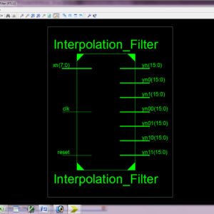
Novel Block-Formulation and Area-Delay-Efficient Reconfigurable Interpolation Filter Architecture for Multi-Standard SDR Applications
Abstract: The input-matrix and the coefficient-matrix resizes when changes. An analysis of interpolation filter computation for different up-sampling factors is made in this paper to identify redundant computations and removed those by reusing partial results. Reuse of partial results eliminates the necessity of matrix resizing in interpolation filter computation. A novel block-formulation is presented to share the partial results for parallel computation of filter outputs of different up-sampling factors. Using the proposed block formulation, to increase the number of tab to 16 and to get the accuracy and reduce the delay. The proposed architecture of this paper analysis the logic size, area and power consumption using Xilinx 14.2.
List of the following materials will be included with the Downloaded Backup:
Obfuscating DSP Circuits via High Level Transformations
This paper presents a novel approach to design obfuscated circuits for digital signal processing (DSP) applications using high-level transformations, a key-based obfuscating finite-state machine (FSM), and a reconfigurator. The goal is to design DSP circuits that are harder to reverse engineer. High level transformations of iterative data-flow graphs have been exploited for area-speed-power tradeoffs. This is the first attempt to develop a design flow to apply high level transformations that not only meet these tradeoffs but also simultaneously obfuscate the architectures both structurally and functionally. Functional obfuscation is accomplished by requiring use of the correct initialization key, and configure data. Structural obfuscation is also achieved by the proposed methodology via high-level transformations. The proposed architecture of this paper analysis the logic size, area and power consumption using Xilinx 14.2
List of the following materials will be included with the Downloaded Backup:
One-Sided Schmitt-Trigger-Based 9T SRAM Cell for Near-Threshold Operation
Abstract:
This paper presents a one-sided Schmitt-trigger based 9T static random access memory cell with low energy consumption and high read stability, write ability, and hold stability yields in a bit-interleaving structure without write-back scheme. The proposed Schmitt-trigger-based 9T static random access memory cell obtains a high read stability yield by using a one-sided Schmitt-trigger inverter with a single bit-line structure. In addition, the write ability yield is improved by applying selective power gating and a Schmitt-trigger inverter write assist technique that controls the trip voltage of the Schmitt-trigger inverter. The proposed Schmitt-trigger-based 9T static random access memory cell has 0.79, 0.77, and 0.79 times the area, and consumes 0.31, 0.68, and 0.90 times the energy of Chang’s 10T, the Schmitt-trigger-based 10T, and MH’s 9T static random access memory cells, respectively, based on 22-nm Fin FET technology.
List of the following materials will be included with the Downloaded Backup:
Optimizing Ternary Multiplier Design with Fast Ternary Adder
Base Paper Abstract:
Existing ternary multiplier designs are difficult to use in ternary systems. Thus, ternary Wallace tree multipliers that reduce the number of transistors by using 4-input ternary adders are proposed to improve the performance of existing ternary multipliers. A ternary carry-select adder is also proposed to reduce the carry propagation delay, used as a carry-chain adder of the Wallace tree. The proposed multipliers are designed with a custom ternary standard cell library synthesized by multi-threshold complementary metal-oxide-semiconductor (CMOS) with a 28 nm process. Power and delay are verified via HSPICE simulation. The proposed 36 × 36 ternary multiplier shows 79.3% power-delay product improvement over the previous ternary multiplier. The proposed 40 × 40 ternary multiplier shows a power-delay product comparable with that of the 64 × 64 binary multiplier synthesized using Synopsys Design Compiler.
List of the following materials will be included with the Downloaded Backup: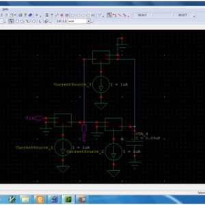
OTA-Based Logarithmic Circuit for Arbitrary Input Signal and Its Application
In this paper, a new design procedure has been proposed for realization of logarithmic function via three phases: 1) differentiation; 2) division; and 3) integration for any arbitrary analog signal. All the basic building blocks, i.e., differentiator, divider, and integrator, are realized by operational transconductance amplifier, a current mode device. Realization of exponential, power law and hyperbolic function as the design examples claims that the proposed synthesis procedure has the potential to design a log-based nonlinear system in a systematic and hierarchical manner. The proposed architecture of this paper area and power consumption analysis using tanner tool.
List of the following materials will be included with the Downloaded Backup: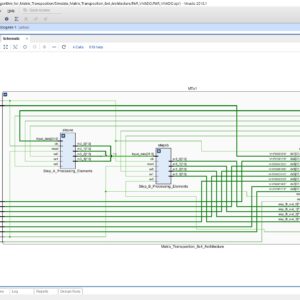
Parallel Pipelined Architecture and Algorithm for Matrix Transposition Using Registers
Base Paper Abstract:
In this brief, we present a new algorithm and architecture for continuous-flow matrix transposition using registers. The algorithm supports P-parallel matrix transposition. The hardware architecture reaches the theoretical minimums in terms of latency and memory. It is composed of a group of identical cascaded basic swap circuits, whose stages are determined by the corresponding algorithm, and can be controlled via a set of counters. Compared with the state-of-the-art architecture, the proposed architecture supports matrices whose rows and columns are integer multiples of P. Here P can be arbitrary, including but not limited to power-of-two integers. Moreover, our results provide additional insight into continuous-flow non-square matrix transposition.
List of the following materials will be included with the Downloaded Backup:
Power Efficient Approximate Divider Architecture for Error Resilient Applications
Base Paper Abstract:
Approximate computing is an emerging paradigm in error-tolerant applications that leads to power-efficient designs without significant loss in quality. The divider in these applications have complex hardware and more latency among the computational blocks resulting in power consumption. Hence approximating the division module would lead to designs with vastly improved power efficiency. A new approximate subtractor (AxSUB) is proposed in this paper with the intent to reduce the hardware complexity while achieving accuracy within permissible limits. The proposed AxSUB and existing approximate subtractor units are used in the restoring array division (RAD) architecture to prove the efficacy of the AxSUB. Comprehensive error and synthesis analysis are performed on RAD architectures implemented using AxSUB, and existing methods. Our proposed design achieved a 21% decrease in area and a 28% decrease in power consumption compared to the exact design. The proposed and existing RAD architectures is implemented on change detection applications to validate the quality-effort tradeoff.
List of the following materials will be included with the Downloaded Backup:
Power Efficient Tiny Yolo CNN Using Reduced Hardware Resources Based on Booth Multiplier and WALLACE Tree Adders
Base Paper Abstract:
Convolutional Neural Network (CNN) has attained high accuracy and it has been widely employed in image recognition tasks. In recent times, deep learning-based modern applications are evolving and it poses a challenge in research and development of hardware implementation. Therefore, hardware optimization for efficient accelerator design of CNN remains a challenging task. A key component of the accelerator design is a processing element (PE) that implements the convolution operation. To reduce the amount of hardware resources and power consumption, this article provides a new processing element design as an alternate solution for hardware implementation. Modified BOOTH encoding (MBE) multiplier and WALLACE tree-based adders are proposed to replace bulky MAC units and typical adder tree respectively. The proposed CNN accelerator design is tested on Zynq-706 FPGA board which achieves a throughput of 87.03 GOP/s for Tiny-YOLO-v2 architecture. The proposed design allows to reduce hardware costs by 24.5% achieving a power efficiency of 61.64 GOP/s/W that outperforms the previous designs.
List of the following materials will be included with the Downloaded Backup: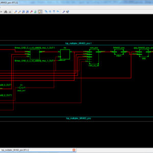
Pre Encoded Multipliers Based on Non Redundant Radix 4 Signed Digit Encoding
Abstract: In this paper we are discussed about the new design of pre-encoded multiplier are explored at offline the standard co efficient and storing them in system memory. The co efficient is used in non redundant radix 4 signed digit form. This encoding technique is less complex partial product implementation and more area and power efficient design. Analysis is verifies the proposed system is efficient from the existing system.
List of the following materials will be included with the Downloaded Backup: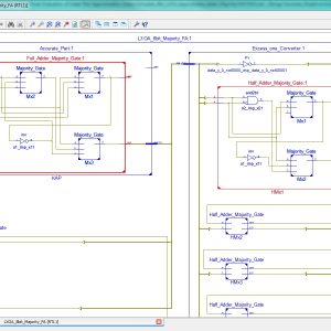
Probability-Driven Evaluation of Lower-Part Approximation Adders
Abstract:
Parallel prefix adder topologies suffer from carry chains forming critical paths, limiting the performance and therefore the efficiency. We study approximation methods that offload the lower-part of calculation to an approximate unit and shorten the carry chain. We derive their accuracy models using probability theory. These models can replace Monte Carlo simulations. Furthermore, they can reveal better accuracy trade-offs without going through the RTL design, synthesis, and simulation of each unit and approximation level individually. Thus, they can eliminate the required design and simulation time and effort. After analyzing area-wise comparisons at varying number of approximated bits, we show that choosing a design that outperforms the others probabilistically also outperforms them in terms of accuracy, power, and performance trade-offs.
List of the following materials will be included with the Downloaded Backup: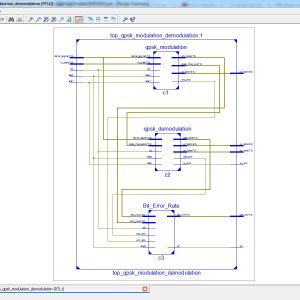
QPSK Modulator on FPGA
Abstract:
The paper presents the theoretical backgrounds of a QPSK Modulation. The QPSK Modulator is then simulated using Modelsim and Xilinx environment tool for FPGA design as well as implemented on a Spartan 6 LX9 FPGA. The modulator algorithm has been implemented on FPGA using the Verilg HDL language on Xilinx ISE 14.2. The local clock oscillator of the board is 50Mhz which corresponds with a period of 20ns. The frequency of the QPSK carrier is 31,250 kHz and because the QPSK symbol is made of two bits, the output frequency is 62,50kbps. The modulator has been designed and simulated and its performances were evaluated by measurements.
List of the following materials will be included with the Downloaded Backup:
Quaternary Logic Lookup Table in Standard CMOS
Abstract: Interconnections are increasingly the dominant contributor to delay, area and energy consumption in CMOS digital circuits. The proposed implementation overcomes several limitations found in previous quaternary implementations published so far, such as the need for special features in the CMOS process or power-hungry current-mode cells. We have to use the 512bit quaternary Look Up Table for high level of operations in the FPGA. The proposed architecture of this paper will be planned to implemented and also analysis the output current, output voltage, area using Xilinx 14.3.
List of the following materials will be included with the Downloaded Backup:
Quaternary Logic Lookup Table in Standard CMOS
Abstract: Interconnections are increasingly the dominant contributor to delay, area and energy consumption in CMOS digital circuits. The proposed implementation overcomes several limitations found in previous quaternary implementations published so far, such as the need for special features in the CMOS process or power-hungry current-mode cells. We have to use the 512bit quaternary Look Up Table for high level of operations in the FPGA.The proposed architecture of this paper will be planned to implemented and also analysis the output current, output voltage, area using Xilinx 14.3.
List of the following materials will be included with the Downloaded Backup:
Radiation-Hardened 0.3–0.9-V Voltage-Scalable 14T SRAM and Peripheral Circuit in 28-nm Technology for Space Applications
Abstract:
Conventional radiation-hardened cells of static random access memory (SRAM) are not robust enough in 28 nm technology, due to partial immunity of single-event upset (SEU) effect (Quatrobased cells) or insufficient critical charges in sensitive nodes (conventional stacked cells). The reduction of read noise margin (RNM) at the low supply voltage (VDD) confines these cells from low VDD applications. We propose a novel interleaving stacked-14T (ILS-14T) cell which prevents voltage transient from propagating to other redundancies. The ILS-14T cell can be resilient to both 0–1 and 1–0 upsets by injecting 12 mA in sensitive nodes. The critical charges of the ILS-14T cell are substantially larger than most other hardened cells at VDD from 0.3 to 0.9 V. The RNM of the ILS-14T cell is two times of most Quatro-based cells at 0.3 V VDD and larger than most cells at 0.6 and 0.9 V VDD. The area of occupation is 334% of the conventional 6T cell, which equals other 14T cells. The static–dynamic decoder array with 20%–40% area penalty and 116%–132% delay of rising edge, when compared with the conventional one, reduces the read failure rate by preventing single event transients (SETs) from propagating to unexpected word lines (WLs).
List of the following materials will be included with the Downloaded Backup:
Radiation-Hardened 14T SRAM Bit cell With Speed and Power Optimized for Space Application
Abstract:
In this paper, a novel radiation-hardened 14-transistor SRAM bit cell with speed and power optimized [radiation-hardened with speed and power optimized (RSP)-14T] for space application is proposed. By circuit- and layout-level optimization design in a 65-nm CMOS technology, the 3-D TCAD mixed-mode simulation results show that the novel structure is provided with increased resilience to single-event upset as well as single-event–multiple-node upsets due to the charge sharing among OFF-transistors. Moreover, the HSPICE simulation results show that the write speed and power consumption of the proposed RSP-14T are improved by ∼65% and ∼50%, respectively, compared with those of the radiation hardened design (RHD)-12T memory cell.
List of the following materials will be included with the Downloaded Backup:
RandShift: An Energy-Efficient Fault Tolerant Method in Secure Nonvolatile Main Memory
Abstract:
In this article, we present a simple, yet energy- and area-efficient method for tolerating the stuck-at faults caused by an endurance issue in secure-resistive main memories. In the proposed method, by employing the random characteristics of the encrypted data encoded by the Advanced Encryption Standard (AES) as well as a rotational shift operation, a large number of memory locations with stuck-at faults could be employed for correctly storing the data. Due to the simple hardware implementation of the proposed method, its energy consumption is considerably smaller than that of other recently proposed methods. The technique may be employed along with other error correction methods, including the error correction code (ECC) and the error correction pointer (ECP). To assess the efficacy of the proposed method, it is implemented in a phase-change memory (PCM)- based main memory system and compared with three error tolerating methods. The results reveal that for a stuck-at fault occurrence rate of 10−2 and with the uncorrected bit error rate of 2 × 10⁻³, the proposed method achieves 82% energy reduction compared to the state-of-the-art method. More generally, using a simulation analysis technique, we show that the fault coverage of the proposed method is similar to that of the state-of-the-art method.
List of the following materials will be included with the Downloaded Backup: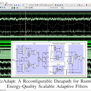
ReAdapt: A Reconfigurable Datapath for Runtime Energy-Quality Scalable Adaptive Filters
Base Paper Abstract:
This paper proposes ReAdapt–a reconfigurable datapath architecture for scaling the energy-quality trade-off of adaptive filtering at runtime. The ReAdapt can dynamically select four adaptive filtering algorithms for gradating complexity levels during runtime by reconfiguring the processing flow in its datapath and by blocking the switching activity (e.g., reducing the CMOS dynamic power) of unused modules with data-gating. The ReAdapt proposal can scale the energy-quality trade-off by choosing the following four different levels of filter algorithms complexity: 1) least mean square (LMS); 2) partial update normalized LMS (PU-NLMS); 3) set-membership normalized LMS (SM-NLMS); 4) normalized LMS (NLMS). The ReAdapt architecture reuses common modules of each adaptive filter, resulting in a compact VLSI hardware implementation. The ReAdapt architecture operation is implemented in a case-study for interference mitigation for electroencephalogram (EEG) signal processing. The hardware synthesis results show an increase of 6.80 times in throughput and at least a reduction of 2.84 times in energy per operation compared with the state-of-the-art adaptive filters. This paper also investigates the benefits of dynamically reconfiguring the four ReAdapt operating modes at runtime for different levels of signal-to-noise ratio (SNR) for the processed signals. We also demonstrate that dynamically reconfiguring the ReAdapt operating modes during runtime results in an optimal energy-quality trade-off which is advantageous over the conventional single static mode.
List of the following materials will be included with the Downloaded Backup:
Reconfigurable Architecture for Real-time Decoding of Canonical Huffman Codes
Base Paper Abstract:
Data compression is an important algorithm which has found its use in modern day algorithms such as Convolutional Neural Networks (CNNs). Reconfigurable platforms (like FPGAs) have strong capabilities to implement time complex tasks like CNNs, however, these algorithms present a big challenge due to high resource demand. Data compression is one of the most utilized techniques to reduce memory utilization in FPGAs. The weights of CNN architecture are usually encoded to store in FPGA. In this paper, we propose design of an efficient decoder based on Canonical Huffman that can be utilized for the efficient decompression of weights in CNN. The proposed design makes use of Hash functions to effectively decode the weights eliminating the need for searching dictionary. The proposed design decodes a single weight in a single clock cycle. Our proposed design has a maximum frequency of 408.97MHz utilizing 1% of system LUTs when tested for Aritix 7 platform.
List of the following materials will be included with the Downloaded Backup: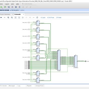
Reconfigurable Digital Delta-Sigma Modulation Transmitter Architecture for Concurrent Multi-Band Transmission
Abstract:
This paper presents a reconfigurable delta-sigma modulation (DSM) architecture for concurrent multi-band transmission. The reconfigurability in terms of carrier spacing and the number of simultaneous carrier transmission is useful for applications such as carrier aggregation in 5G. This paper uses 4th order reconfigurable multi-band DSM (RMB-DSM) such that the zeros of the noise transfer function can be reconfigured to fall at multiple frequencies, where the carriers are being aggregated. The quantization noise between the transmission bands is a critical issue in the case of multi-band transmission. Therefore, a multi-band additional noise shaping (ANS) function is also introduced, which generates notches around each carrier and reduces the noise level between the multiple pass-bands. The proposed scheme has been validated in simulation, as well as in experiment for aggregating up to four 15 MHz long term evolution (LTE) signals with an overall aggregated bandwidth of 60 MHz. Measurement results show a 10-25% improvement in coding efficiency and 15-35 dB improvement in noise level near the operating frequency band using the proposed multiband augmented noise shaping technique, as compared to the standard DSM. The corresponding improvement of 8% in the overall efficiency is observed by using the proposed multi-band augmented noise shaping technique.
List of the following materials will be included with the Downloaded Backup: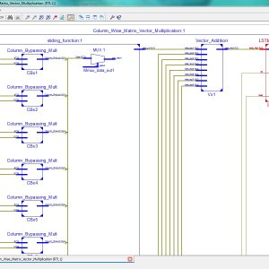
Recurrent Neural Networks With Column-Wise Matrix–Vector Multiplication on FPGAs
Abstract:
This article presents a reconfigurable accelerator for Recurrent Neural networks with fine-grained Column Wise matrix–vector multiplication (RENOWN). We propose a novel latency-hiding architecture for recurrent neural network (RNN) acceleration using column-wise matrix–vector multiplication (MVM) instead of the state-of-the-art row-wise operation. This hardware (HW) architecture can eliminate data dependencies to improve the throughput of RNN inference systems. Besides, we introduce a configurable checkerboard tiling strategy which allows large weight matrices, while incorporating various configurations of element-based parallelism (EP) and vector-based parallelism (VP). These optimizations improve the exploitation of parallelism to increase HW utilization and enhance system throughput. Evaluation results show that our design can achieve over 29.6 tera operations per second (TOPS) which would be among the highest for field-programmable gate array (FPGA)-based RNN designs. Compared to state-of-the-art accelerators on FPGAs, our design achieves 3.7–14.8 times better performance and has the highest HW utilization.
List of the following materials will be included with the Downloaded Backup:
Recursive Approach to the Design of a Parallel Self Timed Adder
Abstract: We are briefly discussed about the 64bit parallel self timed adder based on the recursive formulation. The adder is also based on the asynchronous logic circuit and the transistor is connected in parallel. This adder is chance the path automatically, so the delay is configures automatically. The completion detection unit is given the additional support for practical implementation. The simulation is take place with 130nm CMOS technology for the adder circuit. Finally the power consumption for 64bit adder is 0.29mW.
List of the following materials will be included with the Downloaded Backup: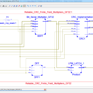
Reliable CRC Based Error Detection Constructions for Finite Field Multipliers With Applications in Cryptography
Abstract:
Finite-field multiplication has received prominent attention in the literature with applications in cryptography and error-detecting codes. For many cryptographic algorithms, this arithmetic operation is a complex, costly, and time-consuming task that may require millions of gates. In this work, we propose efficient hardware architectures based on cyclic redundancy check (CRC) as error-detection schemes for postquantum cryptography (PQC) with case studies for the Luov cryptographic algorithm. Luov was submitted for the National Institute of Standards and Technology (NIST) PQC standardization competition and was advanced to the second round. The CRC polynomials selected are in-line with the required error-detection capabilities and with the field sizes as well. We have developed verification codes through which software implementations of the proposed schemes are performed to verify the derivations of the formulations. Additionally, hardware implementations of the original multipliers with the proposed error-detection schemes are performed over a Xilinx field-programmable gate array (FPGA), verifying that the proposed schemes achieve high error coverage with acceptable overhead.
List of the following materials will be included with the Downloaded Backup:
ReLOPE: Resistive RAM-Based Linear First-Order Partial Differential Equation Solver
Abstract:
Data movement between memory and processing units poses an energy barrier to Von-Neumann-based architectures. In-memory computing (IMC) eliminates this barrier. RRAM-based IMC has been explored for data-intensive applications, such as artificial neural networks and matrix-vector multiplications that are considered as “soft” tasks where performance is a more important factor than accuracy. In “hard” tasks such as partial differential equations (PDEs), accuracy is a determining factor. In this brief, we propose ReLOPE, a fully RRAM crossbar-based IMC to solve PDEs using the Runge–Kutta numerical method with 97% accuracy. ReLOPE expands the operating range of solution by exploiting shifters to shift input data and output data. ReLOPE range of operation and accuracy can be expanded by using fine-grained step sizes by programming other RRAMs on the BL. Compared to software-based PDE solvers, ReLOPE gains 31.4× energy reduction at only 3% accuracy loss.
List of the following materials will be included with the Downloaded Backup:
Resource Efficient SRAM based Ternary Content Addressable Memory
Abstract:
Static random access memory (SRAM)-based ternary content addressable memory (TCAM) offers TCAM functionality by emulating it with SRAM. However, this emulation suffers from reduced memory efficiency while mapping the TCAM table on SRAM units. This is due to the limited capacity of the physical addresses in the SRAM unit. This brief offers a novel memory architecture called a resource-efficient SRAM-based TCAM (REST), which emulates TCAM functionality using optimal resources. The SRAM unit is divided into multiple virtual blocks to store the address information presented in the TCAM table. This approach virtually increases the overall address space of the SRAM unit, mapping a greater portion of the TCAM table in SRAM and increasing the overall emulated TCAM bits/SRAM at the cost of reduced throughput. A 72 × 28-bit REST consumes only one 36-kbit SRAM and a few distributed RAMs via implementation on a Xilinx Kintex-7 field-programmable gate array. It uses only 3.5% of the memory resources compared with a conventional SRAM-based TCAM (hybrid-partitioned TCAM).
List of the following materials will be included with the Downloaded Backup:
Reverse Converter Design via Parallel-Prefix Adders: Novel Components, Methodology, and Implementations
Abstract: The implementation of residue number system reverse converters based on well-known regular and modular parallel prefix adders is analyzed. The VLSI implementation results show a significant delay reduction and area × time2 improvements, all this at the cost of higher power consumption, which is the main reason preventing the use of parallel-prefix adders to achieve high-speed reverse converters in nowadays systems. Hence, to solve the high power consumption problem, novel specific hybrid parallel-prefix-based adder components those provide better tradeoff between delay and power consumption. The power, area and delay of the proposed system are analysis using Xilinx 14.2.
List of the following materials will be included with the Downloaded Backup:
RF Power Gating A Low Power Technique for Adaptive Radios
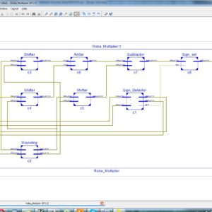
RoBA Multiplier A Rounding Based Approximate Multiplier for High Speed yet Energy Efficient Digital Signal Processing
Abstract:
In this paper, we propose an approximate multiplier that is high speed yet energy efficient. The approach is to round the operands to the nearest exponent of two. This way the computational intensive part of the multiplication is omitted improving speed and energy consumption at the price of a small error. The proposed approach is applicable to both signed and unsigned multiplications. We propose three hardware implementations of the approximate multiplier that includes one for the unsigned and two for the signed operations. The efficiency of the proposed multiplier is evaluated by comparing its performance with those of some approximate and accurate multipliers using different design parameters. In addition, the efficacy of the proposed approximate multiplier is studied in two image processing applications, i.e., image sharpening and smoothing.
List of the following materials will be included with the Downloaded Backup: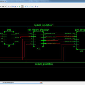
Seizure Prediction using Hilbert Huang Transform on Field Programmable Gate Array
The Hilbert Huang Transform (HHT) has been used extensively in the time-frequency analysis of electroencephalography (EEG) signals and Brain-Computer Interfaces. Most studies utilizing the HHT for extracting features in seizure prediction have used intracranial EEG recordings. Invasive implants in the cortex have unknown long term consequences and pose the risk of complications during surgery. This added risk dimension makes them unsuitable for continuous monitoring as would be the requirement in a Body Area Network. We present an HHT based system on Field Programmable Gate Array (FPGA) for predicting epileptic seizures using scalp EEG. We use bandwidth features of Intrinsic Mode Functions and obtain a classification accuracy of close to 100% using patient-specific classifiers in software. Details of FPGA implementation are also given. The proposed architecture of this paper analysis the logic size, area and power consumption using Xilinx 14.2.
List of the following materials will be included with the Downloaded Backup:
Sharing Logic for Built In Generation of Functional Broadside Tests
Abstract: We are discussed about the built in generation for logic blocks. The advantage of this technique is identifying the similar characteristics of the each logical block. Functional broadside tests are important for addressing overtesting of delay faults as well as avoiding excessive power dissipation during test application. Finally to analysis the performance of the built in generation technique and compare to existing system.
List of the following materials will be included with the Downloaded Backup:
Smart Intelligent and Adaptive Traffic Controller using FPGA
Proposed Abstract:
Traffic management is a critical aspect of modern urban infrastructure, and the ever-increasing volume of vehicles on the road demands innovative and adaptive solutions. This work presents a novel approach to traffic control using Field-Programmable Gate Arrays (FPGAs) as the core technology. The proposed system leverages the capabilities of FPGAs to create a Smart, Intelligent, and Adaptive Traffic Controller that can revolutionize urban traffic management. One of the key features of the proposed work is its adaptability. The system can dynamically adjust traffic signal timings and lane allocations in response to changing traffic patterns of 4-way road conditions with the help of sensor inputs. This methodology adaptability enhances road safety and minimizes traffic delays. The use of FPGA technology in the Traffic controller provides several advantages, including high computational performance, low power consumption, and the ability to reconfigure the system as traffic management needs evolve. Additionally, the system is highly scalable and can be deployed in various urban settings.
List of the following materials will be included with the Downloaded Backup: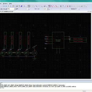
Soft-Error-Aware Read-Stability-Enhanced Low-Power 12T SRAM With Multi-Node Upset Recoverability for Aerospace Applications
Abstract:
With the advancement of technology, the size of transistors and the distance between them are reducing rapidly. Therefore, the critical charge of sensitive nodes is reducing, making SRAM cells, used for aerospace applications, more vulnerable to soft-error. If a radiation particle strikes a sensitive node of the standard 6T SRAM cell, the stored data in the cell are flipped, causing a single-event upset (SEU). Therefore, in this paper, a Soft-Error-Aware Read-Stability-Enhanced Low Power 12T (SARP12T) SRAM cell is proposed to mitigate SEUs. To analyze the relative performance of SARP12T, it is compared with other recently published soft-error-aware SRAM cells, QUCCE12T, QUATRO12T, RHD12T, RHPD12T and RSP14T. All the sensitive nodes of SARP12T can regain their data even if the node values are flipped due to a radiation strike. Furthermore, SARP12T can recover from the effect of single event multi-node upsets (SEMNUs) induced at its storage node pair. Along with these advantages, the proposed cell exhibits the highest read stability, as the ‘0’-storing storage node, which is directly accessed by the bit line during read operation, can recover from any upset. Furthermore, SARP12T consumes the least hold power. SARP12T also exhibits higher write ability and shorter write delay than most of the comparison cells. All these improvements in the proposed cell are obtained by exhibiting only a slightly longer read delay and consuming slightly higher read and write energy.
List of the following materials will be included with the Downloaded Backup:
Source Code Error Detection in High Level Synthesis Functional Verification
A dynamic functional verification method that compares untimed simulations versus timed simulations for synthesizable [high-level synthesis (HLS)] behavioral descriptions (ANSI-C) is presented in this paper. This paper proposes a method that automatically inserts a set of probes into the untimed behavioral description. These probes record the status of internal signals of the behavioral description during an initial untimed simulation. These simulation results are subsequently used as golden outputs for the verification of the internal signals during a timed simulation once the behavioral description has been synthesized using HLS. Our proposed method reports any simulation mismatches and accurately pinpoints any discrepancies between the functional Software (SW) simulation and the timed simulation at the original behavioral description (source code). Our method does not only determine where to place the probes, but is also able to insert different type of probes based on the specified HLS synthesis options in order not to interfere with the HLS process, minimizing the total number of probes and the size of the data to be stored in the trace file in order to minimize the running time. Results show that our proposed method is very effective and extremely simple to use as it is fully automated using Xilinx 14.2.
List of the following materials will be included with the Downloaded Backup:
Sparse FIR Filter Design via Partial 1-Norm Optimization
Abstract:
Electrocardiogram (ECG) is a form of cardiovascular measurement, for the diagnosis of different heart rate conditions. However, numerous noises usually harm the amplitude and time period of the signal from the ECG signal, at following a transition of the analog ECG signal from the sensor module into a digital format. The appropriate digital filter may be used to remove different forms of noise such as Baseline Wander, Power line interference, High frequency noise and Physiological Artifacts. The Digital FIR filter will have prospected to reduced the artifacts in the ECG signals. The signals taken from the MIT-BIH data base which contains the normal and abnormal waveforms. This Digital FIR filter can have more performance by using more TAP numbers such as multiplying, delaying and getting more effectiveness. This proposed work would implement a 1 norm minimization in the FIR filter with liner step method to minimize sparse complexity and reduce the mini-max approximation error for sparse maximization. Given these facts, several rules for selecting indicators of potential zero coefficients to be used in 1 standard optimization are adopted in the proposed algorithm. The efficacy of the proposed design algorithm was developed in Verilog HDL, simulated in Modelsim software and synthesized in Xilinx vertex 5 FPGA, and finally prove all the parameters in terms of area, delay and power.
List of the following materials will be included with the Downloaded Backup: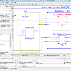
Static Delay Variations Modules For Ripple-Carry and Borrow Save Adders
Abstract:
This paper introduces two statistical delay variability models for certain hardware adder implementations, namely, the ripple-carry adder (RCA) and the borrow-save adder (BSA). The introduced models take into account correlated variation sources. Initially, we derive a first proposed model, namely, Type-I model, in the form of expressions for the computation of the exact Probability Density Functions (PDFS) of maximum output delays for Gaussian and non-Gaussian variation sources. Furthermore, we present closed formulas for the co-variances between output delays of the aforementioned adder architectures. The introduced derived co-variances are subsequently combined with Clark’s method to derive a second proposed model, Type-II model, which comprises approximations of the maximum delay PDF for an RCA and a BSA. Simulation results and the derived exact Type-I PDFs are found to perfectly agree, while the proposed Clark-based Type-II models present an error for standard deviation of maximum delay that increases as BSA word length increases. Both the introduced models and the simulations prove that BSAs achieve narrower delay distributions than RCAs, i.e., they significantly reduce delay variance. Consequently, BSAs are proven to be suitable for variation-tolerant applications by providing a timing safety margin, when compared to RCA architectures. The underlying analysis indicates that for the case of BSA and either intra-die delay variations only or both intra and inter-die delay variations, the Type-II models introduce non negligible errors, which are as much as 16% of the standard deviation of maximum delay for a 256-digit BSA, as the Type II Gaussian PDF approximations deviate significantly from the exact Type-I PDFs. However, for all RCA and BSA inter-die only variation cases, both types present satisfactory accuracy due to the Gaussian shape of exact PDF.
List of the following materials will be included with the Downloaded Backup:
Stochastic Implementation and Analysis of Dynamical Systems Similar to the Logistic Map
Abstract:
Stochastic computing (SC) is a digital computation approach that operates on random bit streams to perform complex tasks with much smaller hardware, with compared to conventional binary radix approaches. It is characterized by its use of pseudo-random numbers implemented by 0-1 sequences called stochastic numbers (SN) are interpreted as probabilities. Accuracy is usually assumed to depend on the interacting SN being highly independent or uncorrelated in a loosely specified way. This paper introduced a new approach of Stochastic and Analysis of Dynamical digital computation with ALU Design. In existing comparison of Floating point ALU Design is not implemented a Stochastic approach, So here the proposed will design to implemented a Stochastic Computing in ALU Design. In top-down design approach of ALU Design, four arithmetic modules, addition, subtraction, multiplication and division are combined to form a Stochastic ALU Unit. Each module is divided into sub-module with two selection bits are combined to select a particular operation. Each module is independent to each other. This modules are realized and validated using VHDL simulation and synthesized in Xilinx 14.2, finally shown the comparison of Area, Power and Delay.
List of the following materials will be included with the Downloaded Backup: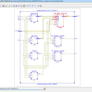
The Mesochronous Dual-Clock FIFO Buffer
Abstract:
To increase system composability and facilitate timing closure, fully synchronous clocking is replaced by more relaxed clocking schemes, such as mesochronous clocking. Under this regime, the modules at the two ends of a mesochronous interface receive the same clock signal, thus operating under the same clock frequency, but the edges of the arriving clock signals may exhibit an unknown phase relationship. In such cases, clock synchronization is needed when sending data across modules. In this brief, we present a novel mesochronous dual-clock first-input– first-output (FIFO) buffer that can handle both clock synchronization and temporary data storage, by synchronizing data implicitly through the explicit synchronization of only the flow-control signals. The proposed design can operate correctly even when the transmitter and the receiver are separated by a long link whose delay cannot fit within the target operating frequency. In such scenarios, the proposed mesochronous FIFO can be extended to support multicycle link delays in a modular manner and with minimal modifications to the baseline architecture. When compared with the other state-of-the-art dual-clock mesochronous FIFO designs, the new architecture is demonstrated to yield a substantially lower cost implementation.
List of the following materials will be included with the Downloaded Backup: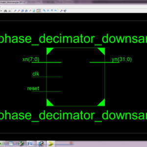
To develop and Implement Low Power, High Speed VLSI for Processing Signals using Multi rate Techniques Low Power Divider Using Vedic Mathematics
Abstract:
Multirate technique is necessary for systems with different input and output sampling rates. Recent advances in mobile computing and communication applications demand low power and high speed VLSI DSP systems. In this paper to discuss the downsampling technique and its improvement, major drawbacks of present approaches possible to increase degeneracy. This Multirate design methodology is systematic and applicable to many problems. The proposed architecture of this paper analysis the logic size, area and power consumption using Xilinx 14.2.The proposed architecture of this paper analysis the logic size, area and power consumption using Xilinx 14.2.
List of the following materials will be included with the Downloaded Backup: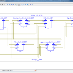
TOSAM: An Energy-Efficient Truncation- and Rounding-Based Scalable Approximate Multiplier
Abstract:
A scalable approximate multiplier, called truncation- and rounding-based scalable approximate multiplier (TOSAM) is presented, which reduces the number of partial products by truncating each of the input operands based on their leading one-bit position. In the proposed design, multiplication is performed by shift, add, and small fixed-width multiplication operations resulting in large improvements in the energy consumption and area occupation compared to those of the exact multiplier. To improve the total accuracy, input operands of the multiplication part are rounded to the nearest odd number. Because input operands are truncated based on their leading one-bit positions, the accuracy becomes weakly dependent on the width of the input operands and the multiplier becomes scalable. Higher improvements in design parameters (e.g., area and energy consumption) can be achieved as the input operand widths increase. To evaluate the efficiency of the proposed approximate multiplier, its design parameters are compared with those of an exact multiplier and some other recently proposed approximate multipliers. Results reveal that the proposed approximate multiplier with a mean absolute relative error in the range of 11%–0.3% improves delay, area, and energy consumption up to 41%, 90%, and 98%, respectively, compared to those of the exact multiplier. It also outperforms other approximate multipliers in terms of speed, area, and energy consumption. The proposed approximate multiplier has an almost Gaussian error distribution with a near-zero mean value. We exploit it in the structure of a JPEG encoder, sharpening, and classification applications. The results indicate that the quality degradation of the output is negligible. In addition, we suggest an accuracy configurable TOSAM where the energy consumption of the multiplication operation can be adjusted based on the minimum required accuracy.
List of the following materials will be included with the Downloaded Backup:
Toward the Multiple Constant Multiplication at Minimal Hardware Cost
Base Paper Abstract:
Multiple Constant Multiplication (MCM) over integers is a frequent operation arising in embedded systems that require highly optimized hardware. An efficient way is to replace costly generic multiplication by bit-shifts and additions, i. e. a multiplier less circuit. In this work, we improve the state of-the-art optimal approach for MCM, based on Integer Linear Programming (ILP). We introduce a new low-level hardware cost metric, which counts the number of one-bit adders and demonstrate that it is strongly correlated with the LUT count. This new model permitted us to consider intermediate truncations that permit to significantly save resources when a full output precision is not required. We incorporate the error propagation rules into our ILP model to guarantee a user-given error bound on the MCM results. The proposed ILP models for multiple flavors of MCM are implemented as an open-source tool and, combined with an automatic code generator, provide a complete coefficient-to-VHDL flow. We evaluate our models in extensive experiments, and propose an in-depth analysis of the impact that design metrics have on synthesized hardware.
List of the following materials will be included with the Downloaded Backup:
Towards Efficient Modular Adders based on Reversible Circuits
Abstract:
Reversible logic is a computing paradigm that has attracted significant attention in recent years due to its properties that lead to ultra-low power and reliable circuits. Reversible circuits are fundamental, for example, for quantum computing. Since addition is a fundamental operation, designing efficient adders is a cornerstone in the research of reversible circuits. Residue Number Systems (RNS) has been as a powerful tool to provide parallel and fault-tolerant implementations of computations where additions and multiplications are dominant. In this paper, for the first time in the literature, we propose the combination of RNS and reversible logic. The parallelism of RNS is leveraged to increase the performance of reversible computational circuits. Being the most fundamental part in any RNS, in this work we propose the implementation of modular adders, namely modulo 2n-1 adders, using reversible logic. Analysis and comparison with traditional logic show that modulo adders can be designed using reversible gates with minimum overhead in comparison to regular reversible adders.
List of the following materials will be included with the Downloaded Backup:
Two Efficient Approximate Unsigned Multipliers by Developing New Configuration for Approximate 4:2 Compressors
Base Paper Abstract:
Approximate computing is a promising approach for reducing power consumption and design complexity in applications that accuracy is not a crucial factor. Approximate multipliers are commonly used in error-tolerant applications. This paper presents three approximate 4:2 compressors and two approximate multiplier designs, aiming at reducing the area and power consumption, while maintaining acceptable accuracy. The paper seeks to develop approximate compressors that align positive and negative approximations for input patterns that have the same probability. Additionally, the proposed compressors are utilized to construct approximate multipliers for different columns of partial products based on the input probabilities of the two compressors in adjacent columns. The proposed approximate multipliers are synthesized using the 28nm technology. Compared to the exact multiplier, the first proposed multiplier improves power × delay and area × power by 91% and 86%, respectively, while the second proposed multiplier improves the two parameters by 90% and 84%, respectively. The performance of the proposed approximate methods was assessed and compared with the existing methods for image multiplication, sharpening, smoothing and edge detection. Also, the performance of the proposed multipliers in the hardware implementation of the neural network was investigated, and the simulation results indicate that the proposed multipliers have appropriate accuracy in these applications.
List of the following materials will be included with the Downloaded Backup: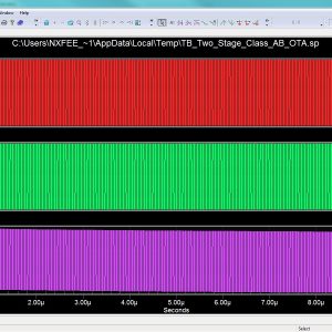
Two-Stage OTA With All Subthreshold MOSFETs and Optimum GBW to DC-Current Ratio
Base Paper Abstract:
An approach for the design of two-stage class AB OTAs with sub-1µA current consumption is proposed and demonstrated. The approach employs MOS transistors operating in subthreshold and allows maximum gain-bandwidth product (GBW) to be achieved for a given DC current budget, by setting optimum distribution of DC currents in the two amplifier stages. Following this strategy, a class AB OTA was designed in a standard 0.5-µm CMOS technology supplied from 1.6-V and experimentally tested. Measured GBW was 307 kHz with 980-nA DC current consumption while driving an output capacitance of 40 pF with an average slew rate of 96 V/ms.
List of the following materials will be included with the Downloaded Backup: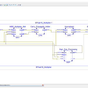
Variable-Precision Approximate Floating-Point Multiplier for Efficient Deep Learning Computation
Base Paper Abstract:
In this brief, a variable-precision approximate floating-point multiplier is proposed for energy efficient deep learning computation. The proposed architecture supports approximate multiplication with BFloat16 format. As the input and output activations of deep learning models usually follow normal distribution, inspired by the posit format, for numbers with different values, different precisions can be applied to represent them. In the proposed architecture, posit encoding is used to change the level of approximation, and the precision of the computation is controlled by the value of product exponent. For large exponent, smaller precision multiplication is applied to mantissa and for small exponent, higher precision computation is applied. Truncation is used as approximate method in the proposed design while the number of bit positions to be truncated is controlled by the values of the product exponent. The proposed design can achieve 19% area reduction and 42% power reduction compared to the normal BFloat16 multiplier. When applying the proposed multiplier in deep learning computation, almost the same accuracy as that of normal BFloat16 multiplier can be achieved.
List of the following materials will be included with the Downloaded Backup:
Vital-Sign Processing Receiver With Clutter Elimination Using Servo Feedback Loop for UWB Pulse Radar System
Abstract:
This brief presents a vital-sign processing circuit for simultaneous dc/near-dc elimination and out-of-band interference rejection without any digital signal processing or algorithm assistance for the ultra wideband (UWB) pulse-based radar system. An intrinsic self balanced MOS diode (SBMD) was proposed as a stable and balanced pseudo resistor applied under a servo feedback loop in a vital-sign receiver of the sensing radar to perform as a high-pass filter (HPF) with an ultralow corner frequency lower than 0.5 Hz for removing undesired clutters of the reflected signals and input dc-offset voltages from innate circuit offsets. A third-order switched-capacitor (SC) Chebyshev low-pass filter (LPF) with leap-frog topology as the subsequent stage was adopted to suppress the out-band noises, thereby establishing an integrated vital-sign processing circuit with band pass frequency response and incorporating it into a radar module to verify its viability.
List of the following materials will be included with the Downloaded Backup:
VLSI Design of SVM-Based Seizure Detection System With On-Chip Learning Capability
Abstract:
Portable automatic seizure detection system is very convenient for epilepsy patients to carry. In order to make the system on-chip trainable with high efficiency and attain high detection accuracy, this paper presents a very large scale integration (VLSI) design based on the nonlinear support vector machine (SVM). The proposed design mainly consists of a feature extraction (FE) module and an SVM module. The FE module performs the three level Daubechies discrete wavelet transform to fit the physiological bands of the electroencephalogram (EEG) signal and extracts the time–frequency domain features reflecting the non stationary signal properties. The SVM module integrates the modified sequential minimal optimization algorithm with the table-driven-based Gaussian kernel to enable efficient on-chip learning. The presented design is verified on an Altera Cyclone II field-programmable gate array and tested using the two publicly available EEG datasets. Experiment results show that the designed VLSI system improves the detection accuracy and training efficiency.
List of the following materials will be included with the Downloaded Backup:Provide Wordlwide Online Support
We can provide Online Support Wordlwide, with proper execution, explanation and additionally provide explanation video file for execution and explanations.
24/7 Support Center
NXFEE, will Provide on 24x7 Online Support, You can call or text at +91 9789443203, or email us nxfee.innovation@gmail.com
Terms & Conditions:
Customer are advice to watch the project video file output, and before the payment to test the requirement, correction will be applicable.
After payment, if any correction in the Project is accepted, but requirement changes is applicable with updated charges based upon the requirement.
After payment the student having doubts, correction, software error, hardware errors, coding doubts are accepted.
Online support will not be given more than 3 times.
On first time explanation we can provide completely with video file support, other 2 we can provide doubt clarifications only.
If any Issue on Software license / System Error we can support and rectify that within end of day.
Extra Charges For duplicate bill copy. Bill must be paid in full, No part payment will be accepted.
After payment, to must send the payment receipt to our email id.
Powered by NXFEE INNOVATION, Pondicherry.
Call us today at : +91 9789443203 or Email us at nxfee.innovation@gmail.com
NXFEE Development & Services

Copyright © 2021 Nxfee Innovation.