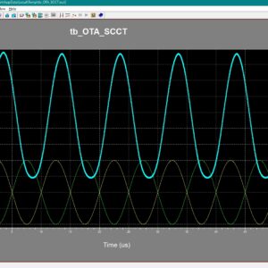
0.4-V nW-Power High-Gain Bulk-Driven Two-Stage OTA With Self-Cascode Composite Transistors
Implementation techniques and results for a recently proposed real-time reconfigurable low-pass equalizer (RLPE) consisting of a variable bandwidth (VBW) filter and a variable equalizer (VE) are presented. Both components utilize fixed finite-length impulse response (FIR) filters combined with a few general multipliers, resulting in lower area and power consumption compared to a general FIR filter, despite requiring more multiplications. This is because the constant multipliers in the fixed FIR filters of the RLPE can be optimized for implementation. An additional advantage is that the proposed RLPE does not require online design. Various implementation alternatives for fixed FIR filters, including ways to increase the frequency, are evaluated to optimize the implementation of the RLPE. Several versions of the proposed RLPE and a general FIR filter for comparison are implemented using a 28-nm fully depleted silicon on insulator (FD-SOI) standard cell library. The results demonstrate that the RLPE baseline design requires less power and area than the general equalizer, and although the frequency of the baseline implementation is lower, the design can reach the same frequency while still having significantly less power and area. Furthermore, an approach is introduced to break the chain in the polynomial section of the VBW filter by using fewer additional registers compared to standard pipelining. Instead, this method reformulates the constant multiplication problem to produce correct results. For the considered case, the power consumption is reduced between 49% and 70% for different frequencies, with an area decrease in the range of 64% to 67%, by using the proposed RLPE compared to a general FIR filter. Index Terms: Constant multiplications, real-time reconfiguration, variable bandwidth (VBW) low-pass filter, variable equalizer (VE).
List of the following materials will be included with the Downloaded Backup:
40-Gb/s 0.7-V 2:1 MUX and 1:2 DEMUX with Transformer-Coupled Technique for SerDes Interface
This paper explores the use of transformer-coupled (TC) technique for the 2:1 MUX and the 1:2 DEMUX to serialize-and-deserialize (SerDes) high-speed data sequence. The widely used current-mode logic (CML) designs of latch and multiplexer/demultiplexer (MUX/DEMUX) are replaced by the proposed TC approach to allow the more headroom and to lower the power consumption. Through the stacked transformer, the input clock pulls down the differential source voltage of the TC latch and the TC multiplexer core while alternating between the two-phase operations. With the enhanced drain-source voltage, the TC design attracts more drain current with less width-to-length ratio of NMOS than that of the CML counterpart. The source-offset voltage is decreased so that the supply voltage can be reduced. The lower supply voltage improves the power consumption and facilitates the integration with low voltage supply SerDes interface. The MUX and the DEMUX chips are fabricated in 65-nm standard CMOS process and operate at 0.7-V supply voltage. The chips are measured up to 40-Gb/s with sub-hundred milliwatts power consumption.
List of the following materials will be included with the Downloaded Backup:
A 0.1–3.5-GHz Duty-Cycle Measurement and Correction Technique in 130-nm CMOS
A duty-cycle correction technique using a novel pulse width modification cell is demonstrated across a frequency range of 100 MHz–3.5 GHz. The technique works at frequencies where most digital techniques implemented in the same technology node fail. An alternative method of making time domain measurements such as duty cycle and rise/fall times from the frequency domain data is introduced. The data are obtained from the equipment that has significantly lower bandwidth than required for measurements in the time domain. An algorithm for the same has been developed and experimentally verified. The correction circuit is implemented in a 0.13-µm CMOS technology and occupies an area of 0.011 mm2. It corrects to a residual error of less than 1%. The extent of correction is limited by the technology at higher frequencies. The proposed architecture of this paper area and power consumption analysis using tanner tool.
List of the following materials will be included with the Downloaded Backup:
A 0.3-V 37-nW 53-dB SNDR Asynchronous Delta–Sigma Modulator in 0.18-μm CMOS
Abstract:
A new solution for an ultralow-voltage bulk driven (BD) asynchronous delta–sigma modulator is described in this paper. While implemented in a standard 0.18-µm CMOS process from the Taiwan Semiconductor Manufacturing Company and supplied with VDD = 0.3 V, the circuit offers a 53.3-dB signal-to-noise and distortion ratio, which corresponds to 8.56-bit resolution. In addition, the total power consumption is 37 nW, the signal bandwidth is 62 Hz, and the resulting power efficiency is 0.79 pJ/conversion. The above-mentioned features have been achieved employing a highly linear transconductor and a hysteretic comparator based on nontailed BD differential pair.
List of the following materials will be included with the Downloaded Backup:
A 13.4-MHz Relaxation Oscillator With Temperature Compensation
Abstract:
A low-phase-noise relaxation oscillator uses a digital compensation loop to reduce its temperature coefficient (TC). This relaxation oscillator is fabricated in the 0.18-µm CMOS process. The measured average oscillation frequency is 13.4 MHz. The whole oscillator consumes 157.8 µW under a 1.2-V supply. The measured average TCs of the oscillation frequency with and without compensation are 193.15 and 1098.7 ppm/◦C, respectively. The TC achieves an improvement of 5.7 times. The measured frequency variation is within ±2% from −20 ◦C to 100 ◦C by using the digital compensation loop. The measured phase noise at 100-kHz offset frequency is −104.82 dBc/Hz, and the measured figure of merit (FOM) is −154.4 dBc/Hz
List of the following materials will be included with the Downloaded Backup:
A 16-bit 2.0-ps Resolution Two-Step TDC in 0.18-μm CMOS Utilizing Pulse-Shrinking Fine Stage
Abstract:
This paper proposes a time-to-digital converter (TDC) that achieves wide input range and fine time resolution at the same time. The proposed TDC utilizes pulse-shrinking (PS) scheme in the second stage for a fine resolution and two-step (TS) architecture for a wide range. The proposed PS TDC prevents an undesirable non-uniform shrinking rate issue in the conventional PS TDCs by utilizing a built-in offset pulse and an offset pulse width detection schemes. With several techniques, including a built-in coarse gain calibration mechanism, the proposed TS architecture overcomes a nonlinearity due to the signal propagation and gain mismatch between coarse and fine stages. The simulation results of the TDC implemented in a 0.18-µm standard CMOS technology demonstrate 2.0-ps resolution and 16-bit range that corresponds to ∼130-ns input time interval with 0.08-mm2 area. It operates at 3.3 MS/s with 18.0 mW from 1.8-V supply and achieves 1.44-ps single-shot precision. Index Terms— Built-in calibration, pulse shrinking (PS), time-to-digital conversion, two step (TS).
List of the following materials will be included with the Downloaded Backup:
A 2.5-V 8-Bit Low power SAR ADC using POLC and SMTCMOS D-FF for IoT Applications
Abstract:
A 2.5-V 8-bit low force and efficient Successive Approximation Register Analog-to-Digital converter (SAR-ADC) utilizing a Principled Open Loop Comparator (POLC) and Switched Multi-Threshold Complementary Metal Oxide Semiconductor (SMTCMOS) D-FF shift Register. In light of high proficiency and low force applications SAR-ADC is increasingly well known, yet it experience the ill effects of resolution and speed confinements. To defeat the above issue proposed a systematic methodology uses low force POLC based SAR-ADC is structured. Considering about the resolution, speed and compact design of 8- bit SAR-ADC, the proposed POLC strategy reasonably diminishes the propagation delay by 37% and decreases the force utilization by 62% appeared differently in relation to the standard system. A D-flip flop is planned to employ SMTCMOS procedure which has low force utilization and productively decline the leakage power. All the above circuits are simulated by using TANNER-EDA tool in 0.25μm CMOS technology produces 97% Efficiency.
List of the following materials will be included with the Downloaded Backup:
A 25-Mb/s 4-ASK Receiver Front-End in 65-nm CMOS for Biomedical Data Telemetry via a Capacitive Link
This brief presents a 25-Mbps 4-amplitude-shiftkeying (4-ASK) receiver front-end (RFE) for biomedical data telemetry via a series-resonant capacitive link. The RFE incorporates low-power clock and data recovery (CDR) circuitry for synchronization in which a novel highly linear trans conductance (Gm) cell is employed in the phase detector (PD) to mitigate any possible error decisions while comparing the phase difference between the input and feedback signals. The proposed RFE is fabricated in 65 nm 1P8M standard CMOS, the core circuit occupies 0.11 mm2, and consumes 2.9 mA from 1 V. While conducting ex vivo measurements using beef tissue and a series-resonant capacitive link, the proposed RFE is capable of processing 4-ASK data patterns up to 25 Mbps with bit error rate (BER) less than 10−3 and total jitter of ∼42 ns. Index Terms Amplitude-shift-keying (ASK), capacitive wireless data transfer (C–WDT), clock and data recovery (CDR), receiver front-end (RFE), series-resonant capacitive link.
List of the following materials will be included with the Downloaded Backup:
A 57.2 nW, 1.3–5 V V IN, –85 dB PSRR, 50 µs Start-Up Time, Bandgap Reference Circuit
This article presents a low-power bandgap reference (BGR) featuring high power supply rejection ratio (PSRR) and fast start-up capability, operating across a wide supply voltage range of 1.3–5 V. A novel pre biased pulse current injection technique is proposed in the start-up circuit, achieving a 1% settling time of 50 µs and a 25× speed gain during start-up. To enhance supply noise immunity, the proposed BGR employs a pre regulated (PR)-based amplifier that effectively decouples the reference voltage from supply voltage fluctuations. Fabricated in a 0.18-µm BCD process, the proposed reference occupies an active area of 0.0394 mm 2. Under a 5 V supply, the circuit generates a 1.2 V reference voltage while consuming only 48 nA quiescent current. Operating down to a minimum supply voltage of 1.3 V, it maintains a low power consumption of 57.2 nW at room temperature. The reference exhibits an average temperature coefficient (TC) of 5.95 ppm/◦C across a wide temperature range (−40◦C to 125◦C) and achieves an outstanding line sensitivity (LS) of 0.00308%/V over the 1.3–5 V supply range. Furthermore, the measured PSRR reaches −85 dB at 100 Hz. Index Terms: Bandgap reference (BGR), pre bias pulse current injection, power supply rejection ratio (PSRR), start-up, ultralow-power (ULP).
List of the following materials will be included with the Downloaded Backup:
A 6-GS/s 6-bit Time Interleaved SAR-ADC
Abstract:
This paper presents a 6-GS/s 6-bit time-interleaved successive approximation register (SAR) analog to digital converter (ADC) realized in 90-nm CMOS. The ADC consists of 32 single SAR-ADCs. The measured effective-number-of-bits (ENOB) at sampling rate of 6.144 GS/s are 5-bit at DC and 3.6-bit at the Nyquist frequency. The power consumption of the ADC-core without I/O’s and 4-to-1 output MUX is 359 mW for an input swing of 1 V peak to peak differential, resulting in a FOM of 4.9 pJ/conv. The proposed design of this Successive approximation register analog to digital converter in Tanner EDA at 65-nm technology and finally proved the comparison of area, power and delay.
List of the following materials will be included with the Downloaded Backup:
A 65-nm CMOS Constant Current Source With Reduced PVT Variation
Abstract:
This paper presents a new nanometer-based low-power constant current reference that attains a small value in the total process–voltage–temperature variation. The circuit architecture is based on the embodiment of a process-tolerant bias current circuit and a scaled process-tracking bias voltage source for the dedicated temperature-compensated voltageto-current conversion in a preregulator loop. Fabricated in a UMC 65-nm CMOS process, it consumes 7.18µWwitha1.4V supply. The measured results indicate that the current reference achieves an average temperature coefficient of 119 ppm/°C over 12 samples in a temperature range from−30 °C to 90 °C without any calibration. Besides, a low line sensitivity of 180 ppm/V is obtained. This paper offers a better sensitivity figure of merit with respect to the reported representative counterparts.
List of the following materials will be included with the Downloaded Backup:
A 7T Security Oriented SRAM Bitcell
Abstract:
Power analysis (PA) attacks have become a serious threat to security systems by enabling secret data extraction through the analysis of the current consumed by the power supply of the system. Embedded memories, often implemented with six-transistor (6T) static random access memory (SRAM) cells, serve as a key component in many of these systems. However, conventional SRAM cells are prone to side-channel power analysis attacks due to the correlation between their current characteristics and written data. To provide resiliency to these types of attacks, we propose a security-oriented 7T SRAM cell, which incorporates an additional transistor to the original 6T SRAM implementation and a two-phase write operation, which significantly reduces the correlation between the stored data and the power consumption during write operations. The proposed 7T SRAM cell was implemented in a 28 nm technology and demonstrates over 1000× lower write energy standard deviation between write ‘1’ and ‘0’ operations compared to a conventional 6T SRAM. In addition, the proposed cell has a 39%–53% write energy reduction and a 19%–38% reduced write delay compared to other power analysis resistant SRAM cells.
List of the following materials will be included with the Downloaded Backup:
A 9T SRAM Computation-in-Memory Architecture with High-Precision MAC
To address the data-intensive demands of modern artificial intelligence (AI) systems, computation-in-memory(CIM) based on static random-access memory (SRAM) has emerged as a promising solution by integrating computing functionality within memory arrays. However, conventional SRAM CIM architectures face two key limitations: low output resistance in single-transistor transmission paths and voltage instability on charge-sharing bitlines. These limitations collectively degrade computational accuracy to 4–5 LSB-level integral nonlinearity (INL), restricting practical deployment. This work proposes a regulated-cascode 9T SRAM cell that enhances analog computation accuracy using a high-impedance transmission path through a cascode configuration and stabilizing the discharge amount of the bitline from a single cell via active feedback regulation. Implemented in Semiconductor Manufacturing International Corporation (SMIC) 55-nm CMOS technology, the proposed cell demonstrates 1.31 LSB INL at 400-mV bitline swing (68.4% improvement versus 4–5 LSB baselines), achieving 66.7% voltage utilization efficiency compared with the conventional 50% limit and 23.04% frequency improvement is achieved compared with the conventional architecture. It also achieves an energy efficiency of 18.47 fJ/bit and a compact area of 2.655 × 1.175 µm, while demonstrating a classification accuracy of 97.7% on the MNIST dataset. Index Terms Analog linearity enhancement, multirow readout, regulated cascode circuits, static random-access memory (SRAM)-based compute-in-memory, voltage utilization efficiency.
List of the following materials will be included with the Downloaded Backup:
A Combined Deblocking Filter and SAO Hardware Architecture for HEVC
Abstract:
The latest video coding standard high-efficiency video coding (HEVC) provides 50% improvement in coding efficiency compared to H.264/AVC to meet the rising demands for video streaming, better video quality, and higher resolution. The deblocking filter (DF) and sample adaptive offset (SAO) play an important role in the HEVC encoder, and the SAO is newly adopted in HEVC. Due to the high throughput requirement in the video encoder, design challenges such as data dependence, external memory traffic, and on-chip memory area become even more critical. To solve these problems, we first propose an interlacing memory organization on the basis of quarter-LCU to resolve the data dependence between vertical and horizontal filtering of DF. The on-chip SRAM area is also reduced to about 25% on the basis of quarter-LCU scheme without throughput loss. We also propose a simplified bitrate estimation method of rate-distortion cost calculation to reduce the computational complexity in the mode decision of SAO. Our proposed hardware architecture of combined DF and SAO is designed for the HEVC intraencoder, and the proposed simplified bitrate estimation method of SAO can be applied to both intra- and intercoding. As a result, our design can support ultrahigh definition 7680 × 4320 at 40 f/s applications at merely 182 MHz working frequency. Total logic gate count is 103.3 K in 65 nm CMOS process.
List of the following materials will be included with the Downloaded Backup:
A Compact 0.3 V Class AB Bulk Driven OTA
Abstract:
In this article, a new solution for an ultralow-voltage (ULV) ultralow-power (ULP) operational transconductance amplifier (OTA) is presented. Thanks to the combination of a low-voltage bulk-driven nontailed differential stage with the multipath Miller zero compensation technique, a simple class AB power-efficient ULV structure has been obtained, which can operate from supply voltages less than the threshold voltages of the employed MOS transistors, while offering rail-to-rail input common-mode range at the same time. The proposed OTA was fabricated using the 180-nm CMOS process from Taiwan Semiconductor Manufacturing Company (TSMC) and can operate from VDD ranging from 0.3 to 0.5 V. The 0.3-V version dissipates only 12.6 nW of power while showing a 64.7-dB voltage gain at 1-Hz, 2.96-kHz gain-bandwidth product, and a 4.15-V/ms average slew-rate at 30-pF load capacitance. The measured results agree well with simulations.
List of the following materials will be included with the Downloaded Backup:
A Comparative Analysis of Multiplier Topologies using Different Vedic Sutras
Abstract: The need of low area and high speed Multiplier is increasing as the need of high speed processors are needed. The multipliers used in Square and cube architecture have to be more efficient in area and also in speed. In this paper a multiplier is implemented based on Nikhilam sutra with binary excess unit. The ripple carry adder in the multiplier architecture increases the speed of addition of partial products. The proposed architecture of this paper analysis the logic size, area and power consumption using Xilinx 14.2.
List of the following materials will be included with the Downloaded Backup:
A Computation and Energy Reduction Technique for HEVC Discrete Cosine Transform
In this paper, a novel computation and energy reduction technique for High Efficiency Video Coding (HEVC) Discrete Cosine Transform (DCT) for all Transform Unit (TU) sizes is proposed. The proposed technique reduces the computational complexity of HEVC DCT significantly at the expense of slight decrease in PSNR and slight increase in bit rate by only calculating several pre-determined low frequency coefficients of TUs and assuming that the remaining coefficients are zero. It reduced the execution time of HEVC HM software encoder up to 12.74%, and it reduced the execution time of DCT operations in HEVC HM software encoder up to 37.27%. In this paper, a low energy HEVC 2D DCT hardware for all TU sizes is also designed and implemented using Verilog HDL. The proposed hardware, in the worst case, can process 53 Ultra HD (7680x4320) video frames per second. The proposed technique reduced the energy consumption of this hardware up to 18.9%. Therefore, it can be used in portable consumer electronics products that require a real-time HEVC encoder. The proposed architecture of this paper analysis the logic size, area and power consumption using Xilinx 14.2.
List of the following materials will be included with the Downloaded Backup: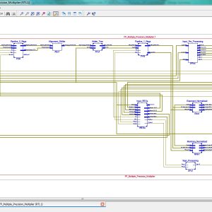
A Configurable Floating Point Multiple Precision Processing Element for HPC and AI Converged Computing
Abstract:
There is an emerging need to design configurable accelerators for the high-performance computing (HPC) and artificial intelligence (AI) applications in different precisions. Thus, the floating-point (FP) processing element (PE), which is the key basic unit of the accelerators, is necessary to meet multiple-precision requirements with energy-efficient operations. However, the existing structures by using high-precision-split (HPS) and low-precision-combination (LPC) methods result in low utilization rate of the multiplication array and long multi term processing period, respectively. In this article, a configurable FP multiple-precision PE design is proposed with the LPC structure. Half precision, single precision, and double precision are supported. The 100% multiplier utilization rate of the multiplication array for all precisions is achieved with improved speed in the comparison and summation process. The proposed design is realized in a 28-nm process with 1.429-GHz clock frequency. Compared with the existing multiple-precision FP methods, the proposed structure achieves 63% and 88% areasaving performance for FP16 and FP32 operations, respectively. The 4× and 20× maximum throughput rates are obtained when compared with fixed FP32 and FP64 operations. Compared with the previous multiple-precision PEs, the proposed one achieves the best energy-efficiency performance with 975.13 GFLOPS/W.
List of the following materials will be included with the Downloaded Backup: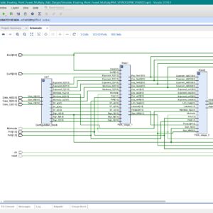
A Configurable Floating-Point Fused Multiply-Add Design with Mixed Precision for AI Accelerators
Base Paper Abstract:
Hardware accelerators for deep learning in artificial intelligence applications must often meet stringent constraints for accuracy and throughput. In addition to architecture/algorithm improvements, high performance computational techniques such as mixed precision are also required. In this paper, a floating-point (FP) fused multiply-add (FMA) unit supporting mixed/multiple precision is proposed. A wide range of conventional FP formats (such as half and single) as well as emerging formats (including E4M3, E5M2, DLFloat, BFLoat16 and TF32) are supported in the proposed design. In addition to all these formats, the proposed design is flexible in manipulating the exponent and mantissa lengths for 8, 16 and 32-bit FP numbers based on the needs of an application. The proposed FMA can be configured to support either multiple normal FMA operations, or alternatively mixed precision in ASIC. It is fully pipelined and in each cycle, the input bit streams are processed based on the provided configuration, so independent of the previous cycles. For normal FMA operations, the proposed design utilizes sharing of resources to parallelize multiple operations based on the available hardware and required precision. For mixed precision the FMA accumulates the lower precision dot products into higher precision to avoid overflow/underflow. It improves computational accuracy by adding all possible dot products at the same time while decreasing the number of rounding operations to prevent rounding errors. An innovative method to accumulate the dot products and the aligned addend is also proposed. By, considering tradeoffs between reusing the available hardware and removing unnecessary complex units, a more efficient and flexible design is attained in terms of hardware metrics and supported different precision computation compared to other designs found in the technical literature. Extensive simulation results for comparative analysis are provided.
List of the following materials will be included with the Downloaded Backup: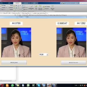
A Deblocking Filter Hardware Architecture for the High Efficiency Video Coding Standard
The new deblocking filter (DF) tool of the next generation High Efficiency Video Coding (HEVC) standard is one of the most time consuming algorithms in video decoding. In order to achieve real-time performance at low-power consumption, we developed a hardware accelerator for this filter. This paper proposes high throughput hardware architecture for HEVC deblocking filter employing hardware reuse to accelerate filtering decision units with a low area cost. Our architecture achieves either higher or equivalent throughput with 5X-6X lower area compared to state of-the-art deblocking filter architectures. The proposed architecture of this paper analysis the logic size, area and power consumption using Xilinx 14.2.
List of the following materials will be included with the Downloaded Backup:
A Decoder for Short BCH Codes With High Decoding Efficiency and Low Power for Emerging Memories
Abstract:
In this paper, a double-error-correcting and triple error-detecting (DEC-TED) Bose–Chaudhuri–Hocquenghem (BCH) code decoder with high decoding efficiency and low power for error correction in emerging memories is presented. To increase the decoding efficiency, we propose an adaptive error correction technique for the DEC-TED BCH code that detects the number of errors in a codeword immediately after syndrome generation and applies a different error correction algorithm depending on the error conditions. With the adaptive error correction technique, the average decoding latency and power consumption are significantly reduced owing to the increased decoding efficiency. To further reduce the power consumption, an invalid-transition-inhibition technique is proposed to remove the invalid transitions caused by glitches of syndrome vectors in the error-finding block. Synthesis results with an industry-compatible 65-nm technology library show that the proposed decoders for the (79, 64, 6) BCH code take only 37%–48% average decoding latency and achieve more than 70% power reduction compared to the conventional fully parallel decoder under the 10−4–10−2 raw bit-error rate.
List of the following materials will be included with the Downloaded Backup:
A Design Implementation and Comparative Analysis of Advanced Encryption Standard (AES) Algorithm on FPGA
Abstract:
As the technology is getting advanced continuously the problem for the security of data is also increasing. The hackers are equipped with new advanced tools and techniques to break any security system. Therefore people are getting more concern about data security. The data security is achieved by either software or hardware implementations. In this work Field Programmable Gate Arrays (FPGA) device is used for hardware implementation since these devices are less complex, more flexible and provide more efficiency. This work focuses on the hardware execution of one of the security algorithms that is the Advanced Encryption Standard (AES) algorithm. The AES algorithm is executed on Vivado 2014.2 ISE Design Suite and the results are observed on 28 nanometers (nm) Artix-7 FPGA. This work discusses the design implementation of the AES algorithm and the resources consumed in implementing the AES design on Artix-7 FPGA. The resources which are consumed are as follows- Slice Register (SR), Look-Up Tables (LUTs), Input/Output (I/O) and Global Buffer (BUFG).
List of the following materials will be included with the Downloaded Backup:
A Design of lightweight true random number generator based on Galois LFSR with dynamic feedback path
Base Paper Abstract:
The Linear Feedback Shift Register (LFSR) is a widely utilized circuit structure in electronic systems, often employed as a Pseudo Random Number Generator (PRNG) for generating pseudo random sequence. However, in light of the significant challenges associated with privacy protection and data encryption, traditional PRNGs have frequently failed to meet the increasing security demands of electronic systems. In contrast, True Random Number Generators (TRNGs), have emerged as essential security primitives within the realm of hardware security, garnering increasing attention. In response to these challenges, this paper proposes a novel lightweight TRNG architecture based on Galois LFSR. This innovation design incorporates inverters and two-to-one multiplexers to modify the feedback path. The proposed structure has been implemented on AMD Xilinx Artix-7 and Kintex-7 FPGA boards. Notably, it demonstrates a resource-efficient design, utilizing only 17 Look-Up Tables (LUTs) and 9 D Flip-Flops (DFFs), while achieving random number with throughput of 300Mbps. Furthermore, the structure successfully passes both randomness test and robustness test, indicating its promising application potential in secure electronic systems.
List of the following materials will be included with the Downloaded Backup: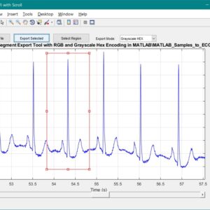
A Dual-Mode ECG Segment Export Tool with RGB and Grayscale Hex Encoding in MATLAB
Project Details :
Electrocardiography (ECG) is a vital non-invasive diagnostic technique used to record the electrical activity of the heart. With increasing emphasis on digital healthcare and remote diagnostics, automated and efficient ECG data handling systems are becoming crucial. This work presents a MATLAB-based Graphical User Interface (GUI) framework designed for interactive ECG waveform analysis, segment selection, image generation, and hexadecimal encoding. The system accepts standard ECG data files in .txt format, processes them for visual inspection, and provides an intuitive scrollable interface to examine long-duration signals. A region of interest can be manually selected using a resizable rectangle tool. Upon selection, the user can export the waveform as a clean image (without axis ticks, titles, or grid lines) in a standardized resolution of 256×256 pixels. To accommodate further integration with embedded systems, AI pipelines, or hardware implementations, the application allows users to convert the exported image into either grayscale or RGB hexadecimal representations. The system supports two modes: RGB HEX (outputs R.txt, G.txt, B.txt) and Grayscale HEX (outputs Grayscale.txt), where each pixel’s intensity is encoded in two-digit hexadecimal format. This dual-format capability is controlled via a dropdown menu for easy toggling. The GUI is fully compatible with MATLAB R2018a and includes legacy support by replacing newer functions (such as writematrix) with older equivalents like dlmwrite. The application provides a real-time, interactive ECG visualization platform while also serving as a data preparation tool for machine learning models, microcontroller visualization, and FPGA-based healthcare signal processing. Its ability to convert waveform data into structured visual and hexadecimal forms bridges the gap between clinical signal acquisition and computational processing. This flexible, open-ended tool is particularly beneficial for researchers working in biomedical signal processing, embedded systems, and AI-based ECG classification.
List of the following materials will be included with the Downloaded Backup:
A Fast and Energy-Efficient Level Shifter with Complementary Output Buffer for Energy-Constrained Systems
This brief presents a 55-nm level shifter (LS) that enables wide voltage range conversion from 80 mV to 1.2 V with high energy efficiency and fast transition speed. The proposed design incorporates a complementary output buffer and an assist discharge path to suppress the short-circuit current and enhance the transition speed. A multi threshold transistor strategy is adopted to expand the input range and reduce static power. Measurement results across 15 samples demonstrate robust subthreshold performance with 4.4-ns transition delay and 49.1-fJ/transition energy during 0.3–1.2-V conversion at 1 MHz. The measured average minimum convertible input voltages are 80 and 139 mV at input frequencies of 50 kHz and 1 MHz, respectively. The compact layout occupies only 7.96 µm 2. Compared to the best benchmarked prior work, the proposed LS achieves 33.8% improvement in energy-delay metrics, making it a highly efficient and scalable solution for energy constrained systems and the Internet of Things (IoT). Index Terms: Current mirror (CM), dual supply, level shifter (LS), low power, subthreshold.
List of the following materials will be included with the Downloaded Backup: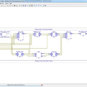
A Floating-Point Fused Dot-Product Unit
Abstract:
A floating-point fused dot-product unit is presented that performs single-precision floating-point multiplication and addition operations on two pairs of data in a time that is only 150% the time required for a conventional floating-point multiplication. When placed and routed in a 45nm process, the fused dot-product unit occupied about 70% of the area needed to implement a parallel dot-product unit using conventional floating-point adders and multipliers. The speed of the fused dot-product is 27% faster than the speed of the conventional parallel approach. The numerical result of the fused unit is more accurate because one rounding operation is needed versus at least three for other approaches.
List of the following materials will be included with the Downloaded Backup:
A Fully Digital Front End Architecture for ECG Acquisition System with 0.5 V Supply
This paper presents a new power-efficient electrocardiogram acquisition system that uses a fully digital architecture to reduce the power consumption and chip area. The proposed architecture is compatible with digital CMOS technology and is capable of operating with a low supply voltage of 0.5 V. In this architecture, no analog block, e.g., low-noise amplifier (LNA), and filters, and no passive elements, such as ac coupling capacitors, are used. A moving average voltage-to time converter is used, which behaves instead of the LNA and anti-aliasing filter. A digital feedback loop is employed to cancel the impact of the dc offset on the circuit, which eliminates the need for coupling capacitors. The proposed architecture of this paper area and power consumption is analysis using tanner tool.
List of the following materials will be included with the Downloaded Backup:
A Fully Static Topologically Compressed 21 Transistor Flip Flop With 75 Percentage of Power Saving
An extremely low-power flip-flop (FF) named topologically-compressed flip-flop (TCFF) is proposed. As compared with conventional FFs, the FF reduces power dissipation by 75% at 0% data activity. This power reduction ratio is the highest among FFs that have been reported so far. The reduction is achieved by applying topological compression method, merger of logically equivalent transistors to an unconventional latch structure. The very small number of transistors, only three, connected to clock signal reduces the power drastically, and the smaller total transistor count assures the same cell area as conventional FFs. In addition, fully static full-swing operation makes the cell tolerant of supply voltage and input slew variation. An experimental chip design with 40 nm CMOS technology shows that almost all conventional FFs are replaceable with proposed FF while preserving the same system performance and layout area. The proposed design is analysis the power and delay by using tanner tools.
List of the following materials will be included with the Downloaded Backup:
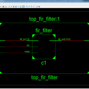
A High Performance FIR Filter Architecture for Fixed and Reconfigurable Applications
Abstract:
Transpose form finite-impulse response (FIR)filters are inherently pipelined and support multiple constant multiplications (MCM) technique that results in significant saving of computation. However, transpose form configuration does not directly support the block processing unlike direct form configuration. In this paper, we explore the possibility of realization of block FIR filter in transpose form configuration for area-delay efficient realization of large order FIR filters for both fixed and reconfigurable applications. Based on a detailed computational analysis of transpose form configuration of FIR filter, we have derived a flow graph for transpose form block FIR filter with optimized register complexity. A generalized block formulation is presented for transpose form FIR filter. We have derived a general multiplier-based architecture for the proposed transpose form block filter for reconfigurable applications. A low-complexity design using the MCM scheme is also presented for the block implementation of fixed FIR filters. The proposed structure involves significantly less area delay product (ADP) and less energy per sample (EPS) than the existing block implementation of direct-form structure for medium or large filter lengths, while for the short-length filters, the block implementation of direct-form FIR structure has less ADP and less EPS than the proposed structure. The proposed architecture of this paper analysis the logic size, area and power consumption using Xilinx 14.2.
List of the following materials will be included with the Downloaded Backup:
A High Resolution FPGA TDC Converter with 2.5 ps Bin Size and -3.79~6.53 LSB Integral Non linearity
Abstract:
As a traditional digital platform, Field Programmable Gate Array (FPGA) is seldom used for analog applications. Since there is no way to fine tune the gate property or circuit structure, the performance of FPGA analog application is usually inferior to its counterparts based on full-custom or even cell-based design. Nevertheless, a high performance FPGA time-to-digital Converter (TDC) is proposed in this paper to expand the FPGA territory into high-end analog applications. The test time signal is sampled by a serious timing references generated by feeding the original clock into a tapped delay line. According to periodicity, the delays among those timing references are wrapped into a single reference period and the effective TDC resolution can be made much smaller than the clock period to compete even with the state-of the art full-custom TDCs in performance. After measurement, the effective resolution is as fine as 2.5 ps. The corresponding differential nonlinearity (DNL) is -1.90~1.66 LSB and the integral nonlinearity (INL) is -3.79~6.53 LSB only.
List of the following materials will be included with the Downloaded Backup:
A High Speed CRC-32 Implementation on FPGA
Base Paper Abstract:
Cyclic Redundancy Check (CRC) is widely used for transmission error detection in various communication interfaces. As the transmission rate increases, accelerating CRC with lower resource consumption for high-speed interfaces becomes significant. This paper analyzes and implements a typical CRC algorithm (Stride-x) and designs a padding-zero strategy to support the input data length with multiples of byte. Besides, experiments are conducted to validate the proposed algorithm on Xilinx FPGA platforms. When stride is 1, the proposed algorithm outperforms a typical parallel CRC algorithm in throughput and resource consumption with various input bus widths (32/128/256 bits).
List of the following materials will be included with the Downloaded Backup:
A High Speed FPGA Implementation of an RSD Based ECC Processor
In this paper, an exportable application-specific instruction-set elliptic curve cryptography processor based on redundant signed digit representation is proposed. The processor employs extensive pipelining techniques for Karatsuba–Ofman method to achieve high throughput multiplication. Furthermore, an efficient modular adder without comparison and a highthrough put modular divider, which results in a short datapath for maximized frequency, are implemented. The processor supports the recommended NIST curve P256 and is based on an extended NIST reduction scheme. The proposed architecture of this paper analysis the logic size, area and power consumption using Xilinx 14.2.
List of the following materials will be included with the Downloaded Backup:
A High-Performance Multiply-Accumulate Unit by Integrating Additions and Accumulations into Partial Product Reduction Process
Abstract:
In this paper, we propose a low-power high-speed pipeline multiply-accumulate (MAC) architecture. In a conventional MAC, carry propagations of additions (including additions in multiplications and additions in accumulations) often lead to large power consumption and large path delay. To resolve this problem, we integrate a part of additions into the pa rtial product reduction (PPR) process. In the proposed MAC architecture, the addition and accumulation of higher significance bits are not performed until the PPR process of the next multiplication. To correctly deal with the overflow in the PPR process, a small-size adder is designed to accumulate the total number of carries. Compared with previous works, experimental results show that the proposed MAC architecture can greatly reduce both power consumption and circuit area under the same timing constraint.
List of the following materials will be included with the Downloaded Backup: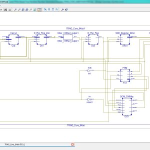
A High-Speed FPGA-based True Random Number Generator using Metastability with Clock Managers
Base Paper Abstract:
True random number generators (TRNGs) are fundamentals in many important security applications. Though they exploit randomness sources that are typical of the analog domain, digital-based solutions are strongly required especially when they have to be implemented on Field Programmable Gate Array (FPGA)-based digital systems. This paper describes a novel methodology to easily design a TRNG on FPGA devices. It exploits the runtime capability of the Digital Clock Manager (DCM) hardware primitives to tune the phase shift between two clock signals. The presented auto-tuning strategy automatically sets the phase difference of two clock signals in order to force on one or more flip-flops (FFs) to enter the metastability region, used as a randomness source. Moreover, a novel use of the fast carry-chain hardware primitive is proposed to further increase the randomness of the generated bits. Finally, an effective on-chip post-processing scheme that does not reduce the TRNG throughput is described. The proposed TRNG architecture has been implemented on the Xilinx Zynq XC7Z020 System on Chip (SoC). It passed all the National Institute of Standards and Technology (NIST) SP 800-22 statistical tests with a maximum throughput of 300×106 bit per second. The latter is considerably higher than the throughput of other previously published DCMbased TRNGs.
List of the following materials will be included with the Downloaded Backup: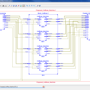
A High-Throughput Hardware Accelerator for Lossless Compression of a DDR4 Command Trace
Abstract:
In a memory system, understanding how the host is stressing the memory is important to improve memory performance. Accordingly, the need for the analysis of memory command trace, which the memory controller sends to the dynamic random access memory, has increased. However, the size of this trace is very large; consequently, a high-throughput hardware (HW) accelerator that can efficiently compress these data in real time is required. This paper proposes a high throughput HW accelerator for lossless compression of the command trace. The proposed HW is designed in a pipeline structure to process Huffman tree generation, encoding, and stream merge. To avoid the HW cost increase owing to high throughput processing, a Huffman tree is efficiently implemented by utilizing static random access memory-based queues and bitmaps. In addition, variable length stream merge is performed at a very low cost by reducing the HW wire width using the mathematical properties of Huffman coding and processing the metadata and the Huffman codeword using FIFO separately. Furthermore, to improve the compression efficiency of the DDR4 memory command, the proposed design includes two preprocessing operations, the “don’t care bits override” and the “bits arrange,” which utilize the operating characteristics of DDR4 memory. The proposed compression architecture with such preprocessing operations achieves a high throughput of 8 GB/s with a compression ratio of 40.13% on average. Moreover, the total HW resource per throughput of the proposed architecture is superior to the previous implementations.
List of the following materials will be included with the Downloaded Backup: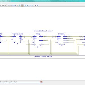
A High-Throughput VLSI Architecture Design of Canonical Huffman Encoder
Abstract:
In this brief, a high-throughput Huffman encoder VLSI architecture based on the Canonical Huffman method is proposed to improve the encoding throughput and decrease the encoding time required by the Huffman code word table construction process. We proposed parallel computing architectures for frequency-statistical sorting and code-size computational sorting. This architecture results in a process of building a tree and assigning symbols that can be completed by scanning the data only once. This solves the problem of the low efficiency of the traditional algorithm, which needs to scan the data twice. Consequently, in addition to the advantages of the high compression ratio inherited from the Canonical Huffman, the proposed architecture has overridden advantages for a high parallelism processing capacity. The experimental results showed that the proposed architecture decreased the encoding time by 26.30% compared to the available Huffman encoder using the standard algorithm when encoding 256 8-bit symbols. Furthermore, the VLSI architecture could further decrease the encoding time when encoding more 8-bit symbols. In particular, when encoding 212,642 8-bit symbols, the proposed VLSI architecture could reduce the encoding time by 87.40%. Thus, compared with the traditional Huffman encoders, this brief achieved the improvement of coding efficiency.
List of the following materials will be included with the Downloaded Backup: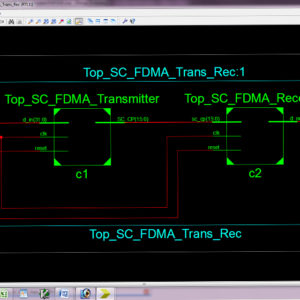
A High-Throughput VLSI Architecture for Hard and Soft SC-FDMA MIMO Detectors
Abstract:
A novel low-complexity multiple-input multiple-output (MIMO) detector tailored for single-carrier frequency division-multiple access (SC-FDMA) systems, suitable for efficient hardware implementations. The proposed detector starts with an initial estimate of the transmitted signal based on a minimum mean square error (MMSE) detector. Subsequently, it recognizes less reliable symbols for which more candidates in the constellation are browsed to improve the initial estimate. The proposed architecture of this paper analysis the logic size, area and power consumption using Xilinx 14.2.
List of the following materials will be included with the Downloaded Backup:
A Highly Efficient Conditional Feed through Pulsed Flip Flop for High Speed Applications
Abstract:
A novel type of highly efficient conditional feed through pulse-triggered flip-flop (P-FF) is proposed and demonstrated. The data-to-output (D-to-Q) delay in this circuit was highly optimized using pre discharging and conditional signal feed through schemes. Power consumption was also reduced using a shared pulse generator and an output feedback-controlled conditional keeper, which diminished the floating status of the internal node. The driving strength of this design was further enhanced by including an additional pull-down path at the output node. Various post layout simulation results applied to 16-nm Fin FET technology demonstrated a higher energy efficiency (at all input data toggle rates) for the proposed topology than comparable P-FF devices. Notably, the proposed model achieved a 62% D-to-Q delay reduction, compared to a transmission gate FF, outperforming the device by more than 66% in terms of power efficiency and 87% in energy efficiency (at a 50% input data toggle rate). Improvements were even more significant in comparison with other conventional P-FFs. These results suggest the proposed design to be a viable new option for high-efficiency sequential elements in high-speed applications.
List of the following materials will be included with the Downloaded Backup:
A Hybrid TRNG PRPG Architecture for Resource Efficient Static Segment and Truncation Multiplier
Reference Paper Abstract:
For error-tolerant applications, low power and small area can be achieved by approximation in calculation with acceptable loss of accuracy. Truncation of lower bits based on the number of significant digits is one of the techniques proposed for approximate multiplier. This paper proposes the area reduction of built-in self-test (BIST) circuitry for an approximate multiplier. The proposed pseudo random pattern generator (PRPG) provides test patterns to the multiplier such that truncation occurs evenly in the input numbers. The fault simulation results show that the proposed circuit can achieve higher fault coverage in the small area overhead required for PRPG. Index Terms: Design for Testability, BIST, PRPG, Approximate Computing, Multiplier
List of the following materials will be included with the Downloaded Backup:
A Hybrid TRNG-PRNG Architecture for High-Performance and Resource-Efficient Random Number Generation on FPGA
Base Paper Abstract:
True random number generators (TRNGs) are fundamentals in many important security applications. Though they exploit randomness sources that are typical of the analog domain, digital-based solutions are strongly required especially when they have to be implemented on Field Programmable Gate Array (FPGA)-based digital systems. This paper describes a novel methodology to easily design a TRNG on FPGA devices. It exploits the runtime capability of the Digital Clock Manager (DCM) hardware primitives to tune the phase shift between two clock signals. The presented auto-tuning strategy automatically sets the phase difference of two clock signals in order to force on one or more flip-flops (FFs) to enter the metastability region, used as a randomness source. Moreover, a novel use of the fast carry-chain hardware primitive is proposed to further increase the randomness of the generated bits. Finally, an effective on-chip post-processing scheme that does not reduce the TRNG throughput is described. The proposed TRNG architecture has been implemented on the Xilinx Zynq XC7Z020 System on Chip (SoC). It passed all the National Institute of Standards and Technology (NIST) SP 800-22 statistical tests with a maximum throughput of 300×106 bit per second. The latter is considerably higher than the throughput of other previously published DCM based TRNGs.
List of the following materials will be included with the Downloaded Backup:
A Lightweight True Random Number Generator for Root of Trust Applications
Base Paper Abstract:
There are many schemes proposed to protect integrated circuits (ICs) against an unauthorized access and usage, or at least to mitigate security risks. They lay foundations for hardware roots of trust whose crucial security primitives are generators of truly random numbers. In particular, such generators are used to yield one-time challenges (nonces) supporting the IC authentication protocols employed to counteract potential threats such as untrusted users accessing ICs. However, IC vendors raise several concerns regarding the complexity of these solutions, both in terms of area overhead, the impact on the design flow, and testability. These concerns have motivated this work presenting a simple, yet effective, all-digital lightweight and self-testable random number generator to produce a nonce. It builds on a generic ring generator architecture, i.e., an area and time optimized version of a linear feedback shift register, driven by a multiple-output ring oscillator. A comprehensive evaluation, based on three statistical test suits from NIST and BSI, show feasibility and efficiency of the proposed scheme and are reported herein.
List of the following materials will be included with the Downloaded Backup:
A Low Complexity I/Q Imbalance Calibration Method for Quadrature Modulator
Abstract:
This brief presents a low-complexity I/Q (in-phase and quadrature components) imbalance calibration method for the transmitter using quadrature modulation. Impairments in analog quadrature modulator have a deleterious effect on the signal fidelity. Among the critical impairments, I/Q imbalance (gain and phase mismatches) deteriorates the residual sideband performance of the analog quadrature modulator degrading the error vector magnitude. Based on the theoretical mismatch analysis of the quadrature modulator, we propose a low-complexity I/Q imbalance extraction algorithm. After the parameter extraction, the transmitter is calibrated by imposing the counter imbalanced mismatch of the transmitter through the digital baseband. In comparison with existing I/Q imbalance calibration methods, the novelty of the proposed method lies in that: 1) only three spectrum measurements of the device-under-test are needed for extraction and calibration of gain and phase mismatches; 2) due to the blind nature of the calibration algorithm, the proposed approach can be readily applicable to an existing I/Q transmitter; 3) no extra hardware that degrades the calibration accuracy is required; and 4) due to the non-iterative nature, the proposed method is faster and computationally more efficient than previously published methods.
List of the following materials will be included with the Downloaded Backup: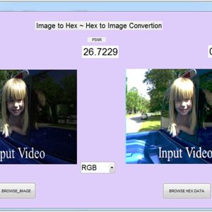
A Low Cost and High Throughtput FPGA Implementation of the Retinex Algorithm for Real Time Video Enhancement
Abstract:
For video applications in a special environment such as medical imaging, space exploration, and underwater exploration, the video captured by an image sensor is often deteriorated because of low lighting conditions. Therefore, it is necessary to enhance the part of the image that is too dark to distinguish details while maintaining the remaining part with the same brightness. The retinex algorithm is widely used to restore naturalness of a video, especially exhibiting outstanding performance in the enhancement of a dark area. However, it demands large computational complexity because of its intricate structure, such as the Gaussian filter and exponentiation operations, and consequently, it is difficult to process in real time. This article presents a low-cost and high-throughput design of the retinex video enhancement algorithm. The hardware (HW) design is implemented using a field-programmable gate array (FPGA), and it supports a throughput of 60 frames/s for a 1920 × 1080 image with negligible latency. The proposed FPGA design minimizes HW resources while maintaining the quality and the performance by using a small line buffer instead of a frame buffer, by applying the concept of approximate computing for the complex Gaussian filter, and by designing a new and nontrivial exponentiation operation. The proposed design makes it possible to significantly reduce HW resources (up to 79.22% of total resources) compared to existing systems and is compatible with commercialized devices through the standard HDMI/DVI video ports.
List of the following materials will be included with the Downloaded Backup: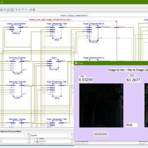
A Low Cost FPGA Implementation of Retinex Based Low-Light Image Enhancement Algorithm
Base Paper Abstract:
Real-time low-light image enhancement has several potential applications, such as advanced driver assistance systems (ADAS), remote sensing, object tracking, etc. The Retinex-based algorithms are mostly used to restore the visibility of low-light images. However, they perform complex mathematical operations over a large spatial window. Consequently, their hardware realization is tedious, and few researchers have attempted to address this problem. In this brief, we propose a Retinex-based algorithm that employs a low-cost edge-preserving filter for illumination estimation. Although certain approximations are used to curtail the hardware logic resource requirement, the quality of the enhanced image is not compromised. The proposed architecture requires only 10868 LUTs and 7409 registers when implemented on ZynQ 7 FPGA. Moreover, it can process HD images (1920×1080) at the rate of 60 frames per second (fps).
List of the following materials will be included with the Downloaded Backup:
A Low Cost Low Power All Digital Spread Spectrum Clock Generator
Abstract:
In this brief, a low-cost low-power all-digital spread spectrum clock generator (ADSSCG) is presented. The proposed ADSSCG can provide an accurate programmable spreading ratio with process, voltage, and temperature variations. To maintain the frequency stability while performing triangular modulation, the fast-relocked mechanism is proposed. The proposed fast-relocked ADSSCG is implemented in a standard performance 90-nm CMOS process, and the active area is 200 µm × 200 µm. The experimental results show that the electromagnetic interference reduction is 14.61 dB with a 0.5% spreading ratio and 19.69 dB with a 2% spreading ratio at 270 MHz The power consumption is 443 µW at 270 MHz with a 1.0 V power supply.
List of the following materials will be included with the Downloaded Backup:
A Low Power and High Speed Voltage Level Shifter Based on a Regulated Cross Coupled Pull Up Network
Abstract:
In this brief, a fast and very low power voltage level shifter (LS) is presented. By using a new regulated cross-coupled (RCC) pull-up network, the switching speed is boosted and the dynamic power consumption is highly reduced. The proposed (LS) has the ability to convert input signals with voltage levels much lower than the threshold voltage of a MOS device to higher nominal supply voltage levels. The presented LS occupies a small silicon area owing to its very low number of elements and is ultra-low-power, making it suitable for low-power applications such as implantable medical devices and wireless sensor networks. Results of the post-layout simulation in a standard 0.18-μm CMOS technology show that the proposed circuit can convert up input voltage levels as low as 80 mV. The power dissipation and propagation delay of the proposed level shifter for a low/high supply voltages of 0.4/1.8 V and input frequency of 1 MHz are 123.1 nW and 23.7 ns, respectively.
List of the following materials will be included with the Downloaded Backup: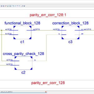
A Low-Complexity Multiple Error Correcting Architecture Using Novel Cross Parity Codes Over GF(2 m)
Abstract: This paper presents a modern low- complexity cross parity code, with a wide range of multiple bit error correction capability at a lower overhead, for improving the reliability. We have to use the two type of error correction technique for 128bit; first one is single bit error correction by using the hamming code. This hamming code is detects and then correct the single bit error correction. Another one is multiple bits error correction by using BCH (Bose–Choudhury– Hocquenghem). This one corrects the multiple bits error. Finally these are implemented and get the simulated result is compared to the previous architecture. The code are simulated and power, area, cost are taken using Xilinx 14.2 software.
List of the following materials will be included with the Downloaded Backup:
A Low-Voltage Radiation-Hardened 13T SRAM Bit cell for Ultralow Power Space Applications
Proposed Abstract:
Continuous transistor scaling, coupled with the growing demand for low-voltage, low-power applications, increases the susceptibility of VLSI circuits to soft-errors, especially when exposed to extreme environmental conditions, such as those encountered by space applications. The most vulnerable of these circuits are memory arrays that cover large areas of the silicon die and often store critical data. Radiation hardening of embedded memory blocks is commonly achieved by implementing extremely large bitcells or redundant arrays and maintaining a relatively high operating voltage; however, in addition to the resulting area overhead, this often limits the minimum operating voltage of the entire system leading to significant power consumption. In this paper, we propose the first radiation-hardened static random access memory (SRAM) bitcell targeted at low-voltage functionality, while maintaining high soft-error robustness. A 32×32 bit memory macro was designed and fabricated in a standard 0.13-µm CMOS process, showing full read and write functionality down to the subthreshold voltage of 300 mV. This is achieved with a cell layout that is only 2×larger than a reference 6T SRAM cell drawn with standard design rules. The proposed architecture of this paper is analysis the logic size, area and power consumption using tanner tool.
List of the following materials will be included with the Downloaded Backup:
A Lower Power Reduced Error Lower Part OR Adder for Multimedia Applications
With the use of multimedia applications, machine learning, and signal processing, approximate computing has become increasingly popular in the pursuit of power-efficient and high-performance architectures for mobile devices. The arithmetic unit is the key component that determines the performance of the overall design. Therefore, in this paper, a novel low-power reduced error lower part-OR adder (RELOA) is proposed. In the proposed architectures, the input bits are divided into three parts, and the sum is computed accurately or approximately based on their significance in the overall sum. The sum of the most significant bits is calculated accurately to have better design metrics, while the least significant bits are approximately to reduce implementation complexity. The proposed architecture offers 16% less power and 9.37% reduction in error metric over existing adders while maintaining a similar delay. Additionally, when processing digital images, the proposed architecture displays good image quality comparable to existing approximate adders.
List of the following materials will be included with the Downloaded Backup:
A Multiuser Detection Algorithm in the Uplink SCFDMA System for Green Communication network
In mobile network the multiuser detection mostly in 5G networks with using communication of CDMA, SC-FDMA, UTMS, EDGE, FDMA, WI-MAX etc,. Here SC-FDMA (Single Carrier FDMA) plays major role in 5G networks even the performance of improving Low Power Consumption in Low Peak to average ratio of RF Signal Transmission. The iteration of signal transmission in the same manner of Multi User SC-FDMA requires traditional parallel and serial interference cancellation algorithm for achieving the result in large, where the algorithm is consumed to be low power consumption. In the same manner to eliminate the Multiple access RF communication, here the proposed algorithm is introduces in named Optical Weighted Parallel Interference Cancellation (OWPIC). As a result to implement the SC-FDMA with high precision then traditional Parallel Interference Cancellation(PIC) with Multi User SC-FDMA using OWPIC, and also implement this architecture in FPGA (S5LX9) and finally analysis the logic size, low power consumption, high frequency interference, radio signal interference.
List of the following materials will be included with the Downloaded Backup:
A Nanopower Biopotential Lowpass Filter Using Subthreshold Current-Reuse Biquads With Bulk Effect Self-Neutralization
Abstract:
A nanopower CMOS 4th-order lowpass filter suitable for biomedical applications is presented. The filter is formed by cascading two types of subthreshold current-reuse biquadratic cell. Each proposed cell is capable of neutralizing the bulk effect that induces the passband attenuation. The nearly 0-dB passband gain can thus be maintained, while the entire filter circuit remains compact and power-efficient. Designed for electrocardiogram detection as an example of application, the filter prototype has been fabricated in a 0.35 µm CMOS process occupying 269 µm × 383 µm chip area. Measurements verify that the filter can operate from a 1.5-V single supply and consumes 5.25 nW, while providing a cutoff frequency of 100 Hz and input-referred noise of 39.38 µVrms. The intermodulation-free dynamic range of 51.48 dB is obtained from a two-tone test of 50 and 60 Hz input frequencies. Compared with state-of-the-art nanopower lowpass filters using the most relevant and reasonable figure of merit, the proposed filter ranks the best.
List of the following materials will be included with the Downloaded Backup: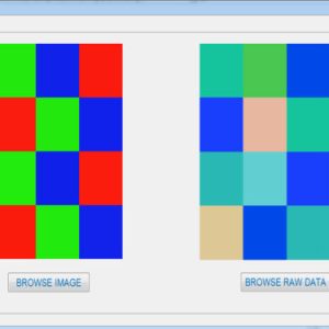
A New Parallel VLSI Architecture for Real-time Electrical Capacitance Tomography
This paper presents a fixed-point reconfigurable parallel VLSI hardware architecture for real-time Electrical Capacitance Tomography (ECT). Another FPGA module performs the inverse steps of the tomography algorithm. A dual port built-in memory banks store the sensitivity matrix, the actual value of the capacitances, and the actual image with RGB format. A two dimensional (2D) core multiprocessing elements (PE) engine intercommunicates with these memory banks via parallel buses. We are focus only on the FPGA module because the design is decide the power consumption and cost. The proposed architecture of this paper analysis the logic size, area and power consumption using Xilinx 14.2.
List of the following materials will be included with the Downloaded Backup:
A Novel Design of Flip-Flop Circuits using Quantum Dot Cellular Automata (QCA)
Abstract:
As the device dimension is shrinking day by day the conventional transistor based CMOS technology encounters serious hindrances due to the physical barriers of the technology such as ultra-thin gate oxides, short channel effects, leakage currents & excessive power dissipation at nano scale regimes. Quantum Dot Cellular Automata is an alternate challenging quantum phenomenon that provides a completely different computational platform to design digital logic circuits using quantum dots confined in the potential well to effectively process and transfer information at nano level as a competitor of traditional CMOS based technology. This paper has demonstrated the implementation of circuits like D, T and JK flip flops using a derived expression from SR flip-flop. The kink energy and energy dissipations has been calculated to determine the robustness of the designed flip-flops. The simulation results have been verified using QCA Designer simulation tool.
List of the following materials will be included with the Downloaded Backup:
A Novel Design of High Speed Multiplier Using Hybrid Adder Technique
Base Paper Abstract:
Electronic devices are necessary in small spaces in order to provide fast speed and low power consumption. Arithmetic operations determine how quickly electronics operate. In many applications involving VLSI signal processing, multiplication is a necessary arithmetic operation. Thus, to create any kind of signal processing module, a high-speed multiplier is a prerequisite. Every individual has different needs and goals, which has led to the development of different multipliers according to the need of application. In this paper, a Hybrid multiplier is proposed and designed using hybrid adders which is a mixture of Brent Kung adder and Kogge Stone adder which results in less delay i.e. 4.062ns compared to other multipliers existed.
List of the following materials will be included with the Downloaded Backup:
A Novel In-Memory Wallace Tree Multiplier Architecture Using Majority Logic
Abstract:
In-memory computing using emerging technologies such as resistive random-access memory (ReRAM) addresses the ‘von Neumann bottleneck’ and strengthens the present research impetus to overcome the memory wall. While many methods have been recently proposed to implement Boolean logic in memory, the latency of arithmetic circuits (adders and consequently multipliers) implemented as a sequence of such Boolean operations increases greatly with bit-width. Existing in-memory multipliers require O(n2) cycles which is inefficient both in terms of latency and energy. In this work, we tackle this exorbitant latency by adopting Wallace Tree multiplier architecture and optimizing the addition operation in each phase of the Wallace Tree. Majority logic primitive was used for addition since it is better than NAND/NOR/IMPLY primitives. Furthermore, high degree of gate-level parallelism is employed at the array level by executing multiple majority gates in the columns of the array. In this manner, an in-memory multiplier of O(n.log(n)) latency is achieved which outperforms all reported in-memory multipliers. Furthermore, the proposed multiplier can be implemented in a regular transistor-accessed memory array without any major modifications to its peripheral circuitry and is also energy-efficient.
List of the following materials will be included with the Downloaded Backup:
A Novel Quantum Dot Cellular Automata X bit × 32 bit SRAM
Application of quantum-dot cellular automata (QCA) technology as an alternative to CMOS technology on the nanoscale has a promising future; QCA is an interesting technology for building memory. The proposed design and simulation of a new memory cell structure based on QCA with a minimum delay, area, and complexity is presented to implement a static random access memory (SRAM). This paper presents the design and simulation of a 16-bit × 32-bit SRAM with a new structure in QCA. Since QCA is a pipeline, this SRAM has a high operating speed. The 16-bit × 32-bit SRAM has a new structure with a 32-bit width designed and implemented in QCA. It has the ability of a conventional logic SRAM that can provide read/write operations frequently with minimum delay. The 16-bit × 32-bit SRAM is generalized and an n × 16-bit × 32-bit SRAM is implemented in QCA. Novel 16-bit decoders and multiplexers (MUXs) in QCA are presented that have been designed with a minimum number of majority gates and cells. The new SRAM, decoders, and MUXs are designed, implemented, and simulated in QCA using a signal distribution network to avoid the coplanar problem of crossing wires. The QCA-based SRAM cell was compared with the SRAM cell based on CMOS. Results show that the proposed SRAM is more efficient in terms of area, complexity, clock frequency, latency, throughput, and power consumption.
List of the following materials will be included with the Downloaded Backup:
A Pipelined Fused Multiply-Add Architecture for Configurable FP16 Multi-Operand Operations
Base Paper Abstract:
Multiple precision modes are needed for a floating-point processing element (PE) because they provide flexibility in handling different types of numerical data with varying levels of precision and performance metrics. Performing high-precision floating-point operations has the benefits of producing highly precise and accurate results while allowing for a greater range of numerical representation. Conversely, low-precision operations offer faster computation speeds and lower power consumption. In this paper, we propose a configurable multi-precision processing element (PE) which supports Half Precision, Single Precision, Double Precision, BrainFloat-16 (BF-16) and TensorFloat-32 (TF-32). The design is realized using GPDK 45 nm technology and operated at 281.9 MHz clock frequency. The design was also implemented on Xilinx ZCU104 FPGA evaluation board. Compared with previous state-of-the-art (SOTA) multiprecision PEs, the proposed design supports two more floating point data formats namely BF-16 and TF-32. It achieves the best energy performance with 2368.91 GFLOPS/W and offers 63% improvement in operating
List of the following materials will be included with the Downloaded Backup:
A Pipelined Reduced Complexity Two Stages Parallel LMS Structure for Adaptive Beam forming
Base Paper Abstract:
In this paper, we propose a reduced complexity parallel least mean square structure (RC-pLMS) for adaptive beamforming and its pipelined hardware implementation. RC-pLMS is formed by two least mean square (LMS) stages operating in parallel (pLMS), where the overall error signal is derived as a combination of individual stage errors. The pLMS is further simplified to remove the second independent set of weights resulting in a reduced complexity pLMS (RC-pLMS) design. In order to obtain a pipelined hardware architecture of our proposed RC-pLMS algorithm, we applied the delay and sum relaxation technique (DRC-pLMS). Convergence, stability and quantization effect analysis are performed to determine the upper bound of the step size and assess the behavior of the system. Computer simulations demonstrate the outstanding performance of the proposed RC-pLMS in providing accelerated convergence and reduced error floor while preserving a LMS identical O(N) complexity, for an antenna array of N elements. Synthesis and implementation results show that the proposed design achieves a significant increase in the maximum operating frequency over other variants with minimal resource usage. Additionally, the resulting beam radiation pattern show that the finite precision DRC-pLMS implementation presents similar behavior of the infinite precision theoretical results.
List of the following materials will be included with the Downloaded Backup: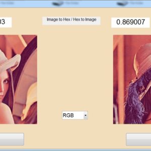
A Real-Time FHD Learning Based Super Resolution System Without a Frame Buffer
Abstract:
The main aim of the Single image (SR) super-resolution is to generate (HR) high-resolution images from (LR) low-resolution images. This paper briefly presents a concept of real time super resolution method of FHD based image extended and scaling processor. The super resolution system includes three blocks of operations. The first is a low-frequency interpolation stage, where bicubic interpolation is used for reconstructing the low-frequency parts of HR images. The second stage generates high-frequency patches by choosing the highest related pre-trained regression function according to each HR low frequency patch. In the third stage, with the high-frequency information, the low-frequency image patches are enhanced and overlapped to construct the SR result. These operations for gaining a high-frequency result are applied to the Y-luminance channel only, while the high-resolution Cb and Cr channels are generated by bicubic interpolation. The proposed system generates the output image resolution of 1920 X 1080 (FHD) by the input of 800 X 800 image size. The proposed architecture performs an anchored neighborhood regression algorithm that generates a high-resolution image from a low-resolution image input using only numbers of line buffers. Finally, super resolution technique is implemented in VHDL and Synthesized in the XILINX VERTEX-5 FPGA and shown the comparison for power, area and delay reports.
List of the following materials will be included with the Downloaded Backup:
A Reliable Low Standby Power 10T SRAM Cell With Expanded Static Noise Margins
Abstract:
This paper explores a low standby power 10T (LP10T) SRAM cell with high read stability and write-ability (RSNM/WSNM/WM). The proposed LP10T SRAM cell uses a strong cross-coupled structure consisting standard inverter with a stacked transistor and Schmitt-trigger inverter with a double-length pull-up transistor. This along with the read path separated from true internal storage nodes eliminates the read-disturbance. Furthermore, it performs its write operation in pseudo differential form through write bit line and control signal with a write-assist technique. To estimate the proposed LP10T SRAM cell’s performance, it is compared with some state-of-the-art SRAM cells using HSPICE in 16-nm CMOS predictive technology model at 0.7 V supply voltage under harsh manufacturing process, voltage, and temperature variations. The proposed SRAM cell offers 4.65X/1.57X/1.46X improvement in RSNM/WSNM/WM and 4.40X/1.69X narrower spread in RSNM/WM compared to the conventional 6T SRAM cell. Furthermore, it shows 1.26X/1.08X/1.01X higher RSNM/WSNM/WM and 1.71X/1.25X tighter/wider spread in RSNM/WM compared to the best studied SRAM cells. The proposed SRAM cell indicates 74.48%/1.41% higher/lower read/write delay compared to the 6T SRAM cell. Moreover, it exhibits the third-(second-) best read (write) dynamic power, consuming 29.69% (26.87%) lower than the 6T SRAM cell. The leakage power is minimized by the proposed design, which is 37.35% and 12.08% lower than that of the 6T and best studied cells, respectively. Nonetheless, the proposed LP10T SRAM cell occupies 1.313X higher area compared to the 6T SRAM cell.
List of the following materials will be included with the Downloaded Backup:
A Reversible Processor Architecture and Its Reversible Logic Design
Proposed Abstract:
This paper presents the design and FPGA implementation of a 16-bit reversible processor architecture employing Fredkin, Feynman, and PERES gate architectures for reversible logic design. Reversible computing offers promising advantages in terms of energy efficiency and information loss prevention, making it suitable for various emerging computing paradigms. The proposed processor architecture encompasses a carefully crafted instruction set, data path, and control logic, all realized using reversible logic gates. Key components such as the ALU, register file, and memory elements are designed with an emphasis on reversibility. The design is implemented using Hardware Description Languages (HDLs), targeting a specific FPGA platform. The paper outlines the design methodology, gate-level implementation details, memory design considerations, FPGA synthesis, and testing procedures. Furthermore, it discusses optimization strategies and presents simulation results to validate the functionality and efficiency of the proposed reversible processor architecture. This work contributes to the advancement of reversible computing and provides insights into the practical realization of reversible processor architectures on FPGA platforms.
List of the following materials will be included with the Downloaded Backup:
A Review on Fundamentals of Ternary Reversible Logic Circuits
Abstract:
One of the main motivations for using ternary logic systems is the amount of information per circuit line is higher as compared to the corresponding binary logic representation, thereby leading to more compact circuit realizations. This is particularly attractive for quantum computing as quarts are expensive resources and minimizing their number is one of the main objectives during synthesis. Therefore, ternary reversible logic synthesis has drawn significant attention among researchers. It deals with fundamental unit of information called quarts that can exist in one of the three states |0, |1 and |2. Hence, the aim of this paper is to bridge the knowledge gap for the beginners in this domain than searching the entire space. Therefore, the present work discusses the basic concepts of ternary reversible logic and ternary reversible gates. The detailed discussion of the various ternary reversible logic synthesis will enable the beginners in this domain to understand the ternary reversible logic in a better way.
List of the following materials will be included with the Downloaded Backup:
A Sub-200nW All-in-One Bandgap Voltage and Current Reference without Amplifiers
Abstract:
This brief presents a low-power and high-precision bandgap voltage and current reference (BGVCR) in one simple circuit for battery-powered applications. All the amplifiers have been eliminated in the proposed circuit. The voltage reference is derived from the bandgap topology, and the current reference is obtained by summing a proportional-to-absolute-temperature (PTAT) current and a complementary-to-absolute-temperature (CTAT) current. Therefore, the temperature coefficient of the current reference can be optimized. Besides, a pseudo-cascode structure and a simple line sensitivity enhancement circuit are adopted to improve the current mirror accuracy and line sensitivity. The proposed circuit is fabricated in a 0.18-μm deep N-well CMOS process with an active area of 0.063 mm2. The measured VREF and IREF are 1.2 V and 51 nA, respectively. The VREF and IREF show measured average temperature coefficients of 32.7 ppm/℃ and 89 ppm/℃ at a temperature of -45 to 125 ℃ and standard deviations of 0.17 % and 1.15 %, respectively. In the supply voltage range of 2 to 5 V, the line sensitivities of voltage and current are 0.058%/V and 1.76%/V, respectively. The minimum supply voltage is 2 V with a total power consumption of 192 nW at room temperature.
List of the following materials will be included with the Downloaded Backup: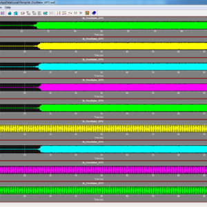
A System of Two Coupled Oscillators With a Continuously Controllable Phase Shift
Abstract:
We present a novel generalization of quadrature oscillators (QVCO) which we call “arbitrary phase oscillator” or APO for short. In contrast to a QVCO which generates only quadrature phases, the APO is capable of continuously generating any desired phase at its output. The proposed structure employs a novel coupling mechanism to generate arbitrary phase shifts between two coupled oscillators without the need for an explicit phase shifter. A rigorous nonlinear dynamic analysis is presented to give a closed-form formula for the generated phase shifts, and the theory is verified by numerical simulation as well as measurement results of a prototype chip fabricated in 130-nm CMOS technology. The prototype APO has a frequency tuning range of 4.90–5.65 GHz and is continuously phase tunable from 0◦ to 360◦ across the entire frequency range. The APO structure can be used in designing novel coupled-oscillator-based phased arrays for 5G wireless communications.
List of the following materials will be included with the Downloaded Backup:
A Thermal Energy Harvesting Power Supply with an Internal Start up Circuit
A complete thermal energy harvesting power supply for implantable pacemakers is presented in this paper. The designed power supply includes an internal startup and does not need any external reference voltage. The startup circuit includes a prestart up charge pump (CP) and a startup boost converter. The prestart up CP consists of an ultralow-voltage oscillator followed by a high-efficiency modified Dickson. Forward body biasing is used to effectively reduce the MOS threshold voltages as well as the supply voltage in oscillator and CP. The steady-state circuit includes a high-efficiency boost converter that utilizes a modified maximum power point tracking scheme. The system is designed so that no failure occurs under overload conditions. Using this approach, a thermal energy harvesting power supply has been designed using 130-nm CMOS technology with low dropout regulator. Finally we are got the output of 2.5V in 10ms.
List of the following materials will be included with the Downloaded Backup:
A Three Stage Comparator and Its Modified Version With Fast Speed and Low Kickback
Abstract:
This brief presents a three-stage comparator and its modified version to improve the speed and reduce the kickback noise. Compared to the traditional two-stage comparators, the three-stage comparator in this work has an extra amplification stage, which enlarges the voltage gain and increases the speed. Unlike the traditional two-stage structure that uses pMOS input pair in the regeneration stage, the three-stage comparator makes it possible to use nMOS input pairs in both the regeneration stage and the amplification stage, further increasing the speed. Furthermore, in the proposed modified version of three-stage comparator, a CMOS input pair is adopted at the amplification stage. This greatly reduces the kickback noise by canceling out the nMOS kickback through the pMOS kickback. It also adds an extra signal path in the regeneration stage, which helps increase the speed further. For easy comparison, both the conventional two-stage and the proposed three-stage comparators are implemented in the same 130-nm CMOS process. Measured results show that the modified version of three-stage comparator improves the speed by 32%, and decreases the kickback noise by ten times. This improvement is not at the cost of increased input referred offset or noise.
List of the following materials will be included with the Downloaded Backup: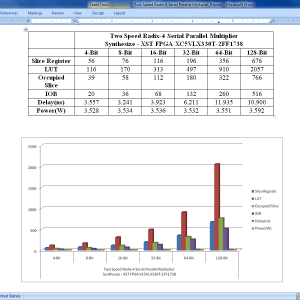
A Two-Speed, Radix-4, Serial–Parallel Multiplier (Booth Multiplier )
Abstract:
In this paper, we present a two-speed, radix-4, serial-parallel multiplier for accelerating applications such as digital filters, artificial neural networks, and other machine learning algorithms. Our multiplier is a variant of the serial–parallel (SP) modified radix-4 Booth multiplier that adds only the nonzero Booth encodings and skips over the zero operations, making the latency dependent on the multiplier value. Two sub circuits with different critical paths are utilized so that throughput and latency are improved for a subset of multiplier values. The multiplier is evaluated on an Intel Cyclone V field-programmable gate array against standard parallel–parallel and SP multipliers across four different process–voltage–temperature corners. We show that for bit widths of 32 and 64, our optimizations can result in a 1.42×–3.36× improvement over the standard parallel Booth multiplier in terms of area–time depending on the input set.
List of the following materials will be included with the Downloaded Backup: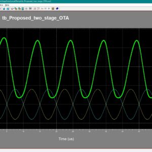
A Two-Stage CMOS Amplifier with High Degree of Stability for All Capacitive Loads
This article presents the conception, design, and realization of a fully differential two-stage CMOS amplifier, that is, unconditionally stable for any value of the capacitive load. This is simply achieved by sending a scaled replica of the output stage current to the amplifier virtual ground in order to create a left half-plane (LHP) zero in the loop gain that either cancels or tracks the output pole in all process, voltage, and temperature (PVT) conditions. Consequently, from a stability point of view, the amplifier behaviour resembles that of a single-pole OTA. Starting from an existing two-stage gain-programmable amplifier, designed in a 0.18-µm bipolar-CMOS-DMOS (BCD) process that was able to drive only 10 pF without encountering into stability issues, a simple circuit has been added to extend the stability to any capacitive load value. An interesting and unusual method, based on the frequency behaviour of the unloaded closed-loop amplifier output impedance, has been introduced to further verify the unconditional stability of this solution. Measurements show a high degree of stability in any load conditions. In the used 0.18-µm BCD technology, silicon area and current consumption of the extra circuit are only 0.0004 mm and 2 µA, respectively, with a 5-V power supply.
List of the following materials will be included with the Downloaded Backup: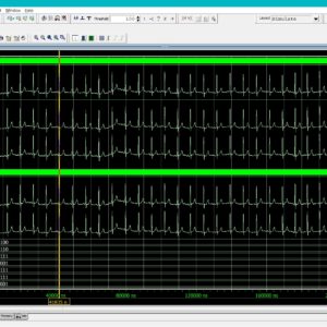
A Unified Approach for Realization of IIR Filters in Delta Domain
Base Paper Abstract:
In this paper, digital realization of IIR filters is concentrated in discrete delta domain. Whenever, a continuous time filter is discretized at fast sampling rate, corresponding discrete time filter in conventional z-domain realization fails to provide meaningful information. In other way, the delta domain based system provides the continuous time results at fast sampling rate leading to the development of a unified method for filter realization in digital domain. Realization of the digital filter using delta operator is having very good finite word length performance under high sampling rate. Three different types of IIR filters are considered for the digital realization in delta domain. The transposed delta direct form II (DDFT-II) structure is used to realize the filters, as it is the most suitable structure for digital filter realization. Butterworth, Chebyshev -2 and Elliptic filters are considered as example and MATLAB Simulink is used to realize the digital filter in delta domain. The frequency
List of the following materials will be included with the Downloaded Backup: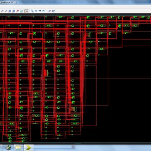
A VLSI Architecture for Watermarking of Gray scale Images using Weighted Median Prediction
Abstract:
Watermarking the digital data is a familiar technique to authenticate and resolve the copyright issues of multimedia data. This paper proposes a new VLSI architecture for watermarking grayscale images using weighted median prediction operation, as this mechanism will have a minimum computation complexity. In this VLSI based data hiding process the secret digital signature is hidden in the host image and analyzed with the PSNR value and Payload capacity.
List of the following materials will be included with the Downloaded Backup: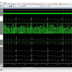
A VLSI-Based Hybrid ECG Compression Scheme for Wearable Sensor Node
Base Paper Abstract:
During smart long-term monitoring of any biomedical signal in wireless body area networks, wearable sensor nodes generate and transmit a large amount of data, increasing transmission power consumption. In order to reduce data storage and power consumption, a lossless data compression technique for an electrocardiogram signal monitoring system is presented in this letter. For this, a hybrid lossless compression algorithm based on Run-length coding and Golomb–Rice coding is proposed to enhance the bit compressing rate. The lossless encoding scheme is implemented on the MIT-BIH arrhythmia database, achieving a compression ratio of 2.91. A VLSI-based architecture of the data compression algorithm is implemented in 90nm CMOS technology that consumes power of 18.78 µW at 100 MHz operating frequency and 1.2 V supply voltage, occupying an area of 0.0051 mm2.
List of the following materials will be included with the Downloaded Backup: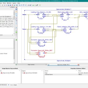
AdAM: Adaptive Approximate Multiplier for Fault Tolerance in DNN Accelerators
Base Paper Abstract:
Deep Neural Network (DNN) hardware accelerators are essential in a spectrum of safety-critical edge-AI applications with stringent reliability, energy efficiency, and latency requirements. Multiplication is the most resource-hungry operation in the neural network’s processing elements. This paper proposes a scalable adaptive fault-tolerant approximate multiplier (AdAM) tailored for ASIC-based DNN accelerators at the algorithm and circuit levels. AdAM employs an adaptive adder that relies on an unconventional use of input Leading One Detector (LOD) values for fault detection by optimizing unutilized adder resources. A gate-level optimized LOD design and a hybrid adder design are also proposed as a part of the adaptive multiplier to improve the hardware performance. The proposed architecture uses a lightweight fault mitigation technique that sets the detected faulty bits to zero. The hardware resource utilization and the DNN accelerator’s reliability metrics are used to compare the proposed solution against the Triple Modular Redundancy (TMR) in multiplication, unprotected exact multiplication, and unprotected approximate multiplication. It is demonstrated that the proposed architecture enables a multiplication with a reliability level close to the multipliers protected by TMR while at the same time utilizing 2.74× less area and with 39.06% less power-delay product compared to the exact multiplier. Moreover, it has similar area, delay, and power consumption parameters compared to the state-of-the-art approximate multipliers with similar accuracy while providing fault detection and mitigation capability. Index Terms Deep neural networks, approximate computing, circuit design, reliability, DNN accelerator.
List of the following materials will be included with the Downloaded Backup: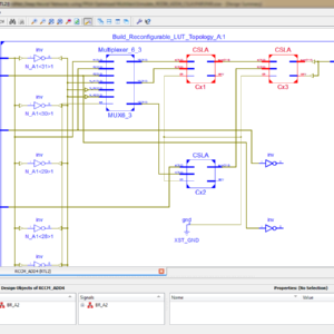
AddNet: Deep Neural Networks Using FPGA-Optimized Multipliers
Abstract:
Low-precision arithmetic operations to accelerate deep-learning applications on field-programmable gate arrays (FPGAs) have been studied extensively, because they offer the potential to save silicon area or increase throughput. However, these benefits come at the cost of a decrease in accuracy. In this article, we demonstrate that reconfigurable constant coefficient multipliers (RCCMs) offer a better alternative for saving the silicon area than utilizing low-precision arithmetic. RCCMs multiply input values by a restricted choice of coefficients using only adders, subtractors, bit shifts, and multiplexers (MUXes), meaning that they can be heavily optimized for FPGAs. We propose a family of RCCMs tailored to FPGA logic elements to ensure their efficient utilization. To minimize information loss from quantization, we then develop novel training techniques that map the possible coefficient representations of the RCCMs to neural network weight parameter distributions. This enables the usage of the RCCMs in hardware, while maintaining high accuracy. We demonstrate the benefits of these techniques using AlexNet, ResNet-18, and ResNet-50 networks. The resulting implementations achieve up to 50% resource savings over traditional 8-bit quantized networks, translating to significant speedups and power savings. Our RCCM with the lowest resource requirements exceeds 6-bit fixed point accuracy, while all other implementations with RCCMs achieve at least similar accuracy to an 8-bit uniformly quantized design, while achieving significant resource savings.
List of the following materials will be included with the Downloaded Backup: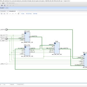
Advanced Encryption Standard Algorithm with Optimal S-box and Automated Key Generation
Base Paper Abstract:
Advanced Encryption Standard (AES) algorithm plays an important role in a data security application. In general S-box module in AES will give maximum confusion and diffusion measures during AES encryption and cause significant path delay overhead. In most cases, either LUTs or embedded memories are used for S- box computations which are vulnerable to attacks that pose a serious risk to real-world applications. In this paper, implementation of the composite field arithmetic-based Sub-bytes and inverse Sub-bytes operations in AES is done. The proposed work includes an efficient multiple round AES cryptosystem with higher-order transformation and composite field s-box formulation with some possible inner stage pipelining schemes which can be used for throughput rate enhancement along with path delay optimization. Finally, input biometric-driven key generation schemes are used for formulating the cipher key dynamically, which provides a higher degree of security for the computing devices.
List of the following materials will be included with the Downloaded Backup: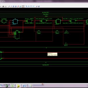
Algorithm and Architecture for a Low Power Content Addressable Memory Based on Sparse Clustered Networks
Abstract: We propose a low-power content-addressable memory (CAM) employing a new algorithm for associativity between the input tag and the corresponding address of the output data of 128bit. The proposed architecture is based on a recently developed sparse clustered network using binary connections that on-average eliminates most of the parallel comparisons performed during a search. Therefore, the dynamic energy consumption of the proposed design is significantly lower compared with that of a conventional low-power CAM design. Given an input tag, the proposed architecture computes a few possibilities for the location of the matched tag and performs the comparisons on them to locate a single valid match. A design methodology based on the silicon area and power budgets, and performance requirements is discussed. The proposed architecture of this paper will be analysis the logic size, area and power consumption using Xilinx 14.2.
List of the following materials will be included with the Downloaded Backup:
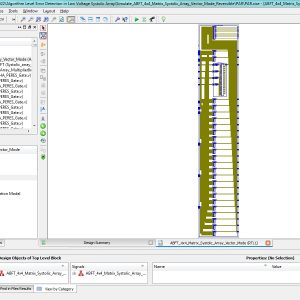
Algorithm Level Error Detection in Low Voltage Systolic Array
Base Paper Abstract:
In this brief an approach is proposed to achieve energy savings from reduced voltage operation. The solution detects timing-errors by integrating Algorithm Based Fault Tolerance (ABFT) into a digital architecture. The approach has been studied with a systolic array matrix multiplier operating at reduced voltages, detecting errors on-the-fly to avoid energy demanding memory round-trips. The analysis of the solution has been done using analog-digital co-simulation to extract the transient behavior under different voltages and clock frequencies. HSPICE simulations using 90nm CMOS transistor models, and experiments by reducing operation voltage of an FPGA device were carried out. HSPICE simulations, showed possibility of 10x increase in energy-efficiency by approaching near-threshold region.
List of the following materials will be included with the Downloaded Backup:
An Aadhaar-Authenticated FPGA-Based Electronic Voting Machine with EPIC Key Derived
Base paper Abstract:
Electronic voting machines are widely used to improve election transparency, reduce manual effort, and provide faster result declaration when compared to traditional paper-based voting systems. The integration of digital platforms further enables ease of access, efficient data handling, and automated vote counting. However, existing electronic voting solutions still face critical challenges such as voter impersonation, data tampering, weak software-based security, and lack of strong hardware-level protection, especially when sensitive voter identity information is involved. Most current systems rely on microcontroller-based architectures, centralized databases, or conventional cryptographic algorithms, which introduce vulnerabilities related to key management, higher computational cost, and limited resistance to physical and logical attacks. To address these issues, this work proposes an Aadhaar-authenticated FPGA-based electronic voting machine with EPIC key–derived lightweight cryptographic vote protection. In the proposed system, Aadhaar number and Voter ID (EPIC) information are captured through a MATLAB-based graphical user interface and securely stored as voter records. The EPIC number is used to derive an 80-bit cryptographic key, while the complete voter information is formatted into a 256-bit data frame and processed within FPGA block memory. Lightweight PRESENT cipher encryption, along with cipher and key shuffling techniques, is employed to protect voter data at the hardware level, ensuring confidentiality and integrity. Decryption is performed using a reverse process to enable authenticated vote verification and result checking without exposing encrypted data. The novelty of this work lies in EPIC key–based dynamic key generation combined with FPGA-based lightweight cryptography, eliminating external key storage and reducing attack surfaces. The system ensures secure authentication, tamper resistance, low resource utilization, and reliable vote verification. Performance and functionality are validated using MATLAB for GUI and data handling, and Verilog HDL for FPGA implementation, demonstrating a secure, efficient, and hardware-trusted electronic voting solution.
List of the following materials will be included with the Downloaded Backup: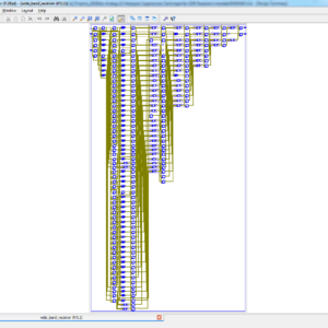
An Analog LO Harmonic Suppression Technique for SDR Receivers
Abstract:
A low-complexity analog technique to suppress the local oscillator (LO) harmonics in software-defined radios is presented. Accurate mathematical analyses show that an effective attenuation of the LO harmonics is achieved by modulating the transconductance of the low-noise transconductance amplifier (LNTA) with a raised-cosine signal. This modulation is performed through the bias network of a cascode device with a negligible increase in the LNTA noise figure. The proposed technique results in a notch at the third harmonic and at least 36 dB of attenuation at the fifth and the seventh harmonics. Experimental results in 130-nm CMOS and post layout simulation results in 65-nm CMOS verify the proper functionality of the proposed technique and the accuracy of the proposed analyses
List of the following materials will be included with the Downloaded Backup: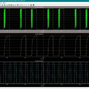
An Area-Efficient Fractional Output Divider Based on Foreground DTC INL Calibration
This brief presents a fractional output divider (FOD) with a foreground digital-to-time converter (DTC) INL calibration scheme. This calibration scheme adjusts the delay control words of two main DTCs (mDTCs) to enable mutual comparison between them. By using a sign-least-mean-squares (sign-LMS) algorithm, the INL error codes are obtained and subsequently applied to a calibration DTC (cDTC) to compensate for the mDTC INL. The prototype occupies a compact core area of 0.01mm2 and operates at a 0.9V supply with a power consumption of 3.6mW at 500MHz. Measurements demonstrate an integrated jitter of 512fs (10kHz to 20MHz) and spur level of -70dBc at 123.46MHz. Index Terms—Fractional output divider (FOD), frequency synthesis, digital-to-time converter (DTC), integral nonlinearity (INL), foreground calibration, bang-bang phase detector (BBPD).
List of the following materials will be included with the Downloaded Backup: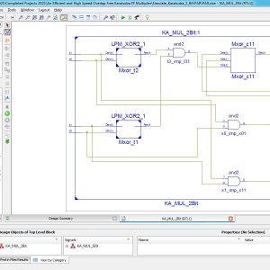
An Efficient and High Speed Overlap Free Karatsuba Based Finite Field Multiplier for FPGA Implementation
Abstract:
Cryptography systems have become inseparable parts of almost every communication device. Among cryptography algorithms, public-key cryptography, and in particular elliptic curve cryptography (ECC), has become the most dominant protocol at this time. In ECC systems, polynomial multiplication is considered to be the most slow and area consuming operation. This article proposes a novel hardware architecture for efficient field-programmable gate array (FPGA) implementation of Finite field multipliers for ECC. Proposed hardware was implemented on different FPGA devices for various operand sizes, and performance parameters were determined. Comparing to state-of-the art works, the proposed method resulted in a lower combinational delay and area–delay product indicating the efficiency of design.
List of the following materials will be included with the Downloaded Backup: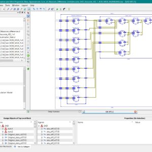
An Efficient Approximate Sum of Absolute Differences Hardware for FPGAs
Proposed Abstract:
Sum of Absolute Differences (SAD) is mainly applied in block-matching tasks such as motion estimation for video compression, stereo matching for depth/disparity calculation, template matching in image/object detection, image registration (including medical imaging), and lightweight optical-flow/tracking systems, because it is simple, fast, and hardware-friendly. The Traditional accurate SAD hardware provides exact results but consumes high power and requires large area, while existing approximate designs reduce cost but often suffer from high errors and poor FPGA-specific optimization. To overcome these limitations, this work proposes an improved SAD hardware architecture that replaces the conventional full adder with a lightweight XOR–MUX structure. This change reduces delay, minimizes area, and increases speed by removing redundant logic and optimizing FPGA resource utilization. The novelty of the design lies in combining approximation with FPGA-aware optimization, achieving bounded error, reduced power consumption, and higher operating frequency. The proposed system is implemented in Verilog HDL and tested on a Xilinx FPGA, showing improvements in LUT usage, clock frequency, and power efficiency, making it suitable for real-time video and image processing applications.
List of the following materials will be included with the Downloaded Backup: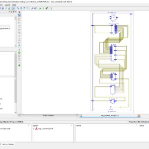
An Efficient Constant Multiplier Architecture Based on Vertical-Horizontal Binary Common Sub-expression Elimination Algorithm for Reconfigurable FIR Filter Synthesis.
Abstract: This paper proposes efficient constant multiplier architecture based on vertical-horizontal binary common sub-expression elimination (VHBCSE) algorithm for designing a reconfigurable finite impulse response (FIR) filter whose coefficients can dynamically change in real time. To design an efficient reconfigurable FIR filter, according to the proposed VHBCSE algorithm, 2-bit binary common sub-expression elimination (BCSE) algorithm has been applied vertically across adjacent coefficients on the 2-D space of the coefficient matrix initially, followed by applying variable-bit BCSE algorithm horizontally within each coefficient. Faithfully rounded truncated multiple constant multiplication/accumulation (MCMAT) and multi-root binary partition graph (MBPG) respectively. Efficiency shown by the results of comparing the FPGA and ASIC implementations of the reconfigurable FIR filter designed using VHBCSE algorithm based constant multiplier establishes the suitability of the proposed algorithm for efficient fixed point reconfigurable FIR filter synthesis.
List of the following materials will be included with the Downloaded Backup: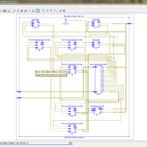
An Efficient Design for Reversible Wallace Unsigned Multiplier
Abstract:
Today, reversible logic can be used for designing low-power CMOS circuits, optical data processing, DNA computations, biological researches, quantum circuits and nanotechnology. Sometimes using of reversible logic is inevitable such as build quantum computers. Reversible logic circuits structure is much more complicated than irreversible logic circuits. Multiplication operation is considered as one of the most important operations in the ALU unit. In this paper, we have proposed two 4×4 reversible unsigned multiplier circuits in which Wallace tree method is used to reduce the depth of circuits. In first design, the partial products circuit is designed using TG and FG gates so that TG is used to produce the partial products and FG for fan-out. In the second design, TG and PG gates are used to produce the partial products and no fan-out is required. Moreover, we have used PG gate and Feynman' block as reversible half-adder (HA) and full-adder (FA) in the summation network, respectively. In the first design, the main purpose is to decrease the depth of the circuit and increase the circuit speed. In the second design we would attempt to improve quantum parameters the number of garbage outputs, constant inputs and quantum cost. The evaluation results show that the first design, in terms of delay, is the fastest circuit. Also, the second design in terms of the number of constant inputs, garbage outputs and quantum cost is better than other designs.
List of the following materials will be included with the Downloaded Backup: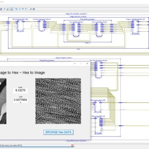
An Efficient Image Encryption Algorithm Based on Innovative DES Structure and Hyperchaotic Keys
Base Paper Abstract:
In fact, as a traditional encryption method, DES has been certified as an unsuitable tool for ciphering due to its smaller key space. Further, in concern of the real-time encryption in the current fast communication era, such as 5G, long-time as well as large computational level processes are not gotten into the consideration. As a result, an innovative encryption structure with hyperchaotic keys for efficient encryption is constructed, where the frame of DES structure is applied, the plain image is shuffled through row and column directions in the first round, and then rearranged to be 64 blocks to fit into the frame of DES structure for 4 rounds ciphering with hyperchaotic subkeys. Also, in order to encrypt the content of the image at the block level, a set of alternative S-box has been produced in this article as well. The simulation results indicate that the proposed scheme is feasible and reliable for digital image encrypting, not only a large key space can be obtained, but also the low correlation of the adjacent contents can be achieved, and further, in comparison of several existing approaches, less-computational resource can be proven as well. In particular, due to the innovative DES structure, the computational speed is significantly faster than the original DES algorithm and many other chaos-based image ciphering schemes.
List of the following materials will be included with the Downloaded Backup: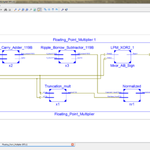
An Efficient Implementation of Floating Point Multiplier
Abstract:
In this paper we describe an efficient implementation of an IEEE 754 single precision floating point multiplier targeted for Xilinx Virtex-5 FPGA. VHDL is used to implement a technology-independent pipelined design. The multiplier implementation handles the overflow and underflow cases. Rounding is not implemented to give more precision when using the multiplier in a Multiply and Accumulate (MAC) unit. With latency of three clock cycles the design achieves 301 MFLOPs. The multiplier was verified against Xilinx floating point multiplier core.
List of the following materials will be included with the Downloaded Backup: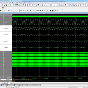
An Efficient VLSI Architecture for Convolution Based DWT Using MAC
Abstract:
The modern real time applications related to image processing and etc., demand high performance discrete wavelet transform (DWT). This paper proposes the floating point multiply accumulate circuit (MAC) based 1D/2D-DWT, where the MAC is used to find the outputs of high/low pass FIR filters. The proposed technique is implemented with 45 nm CMOS technology and the results are compared with various existing techniques. The proposed 8 × 8-point floating point 2-levels 2D-DWT achieves 27.6% and 83.7% of reduction in total area and net power respectively as compared with existing DWT.
List of the following materials will be included with the Downloaded Backup:
An Efficient VLSI Architecture of a Reconfigurable Pulse Shaping FIR Interpolation
This brief proposes a two-step optimization technique for designing a reconfigurable VLSI architecture of an interpolation filter for multi-standard digital up converter (DUC) to reduce the power and area consumption. The proposed technique initially reduces the number of multiplications per input sample and additions per input sample by 83% in comparison with individual implementation of each standard’s filter while designing a root-raised-cosine finite-impulse response filter for multi-standard DUC for three different standards. In the next step, a 2-bit binary common sub-expression (BCS)-based BCS elimination algorithm has been proposed to design an efficient constant multiplier, which is the basic element of any filter. This technique has succeeded in reducing the area and power usage by 41% and 38%, respectively, along with 36% improvement in operating frequency over a 3-bit BCS-based technique reported earlier, and can be considered more appropriate for designing the multi-standard DUC. The proposed architecture of this paper analysis the logic size, area and power consumption using Xilinx 14.2.
List of the following materials will be included with the Downloaded Backup:
An Innovative Area Efficient Pixel Shuffling Method for Image Encryption Algorithm
Proposed Abstract:
In image processing and computer vision, pixel shuffling is a method used to increase an image's resolution without adding more parameters or network complexity. With this technique, a low-quality image's pixels are rearranged to produce an output with a better resolution. Pixel shuffling has proven successful in a number of applications, such as image synthesis, super-resolution, and style transfer. Its simplicity and efficiency make it an attractive option for tasks where increasing image resolution is essential, while avoiding the computational overhead associated with more complex architectures. The image line buffer based pixel shuffling technique presented in this study is an alternative to the classic method, which takes up more logic space in VLSI implementations. This proposed method splits and reconstructs the source photos using a 5x5 image line buffer. With the use of block interleave techniques, this pixel shuffling approach handled row and column sequence using this 5x5 picture line buffer. In conclusion, this study was compared with the PSNR and SSIM value; comparisons of logic sizes for area, latency, and power were also examined.
List of the following materials will be included with the Downloaded Backup: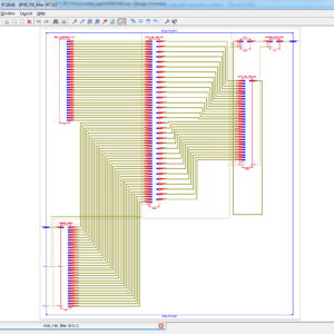
An LUT Based RNS FIR Filter Implementation for Reconfigurable Applications
Abstract:
In this work, two approaches to realize a look up table (LUT) based finite impulse response (FIR) filter using Residue Number System (RNS) are proposed. The proposed implementations take advantage of shift and add approach offered by the chosen module set. The two proposed filter architecture are compared with an earlier proposed version of reconfigurable RNS FIR filter. The filters are synthesized using Cadence RTL compiler in UMC 90 nm technology. The performance of the filters are compared in terms of Area (A), Power (P), and Delay (T). The results show that one of the proposed architecture offers significant improvement in terms of delay, while the second approach is well suited for applications that require minimal power and area. Both implementations offer advantage in area delay and power-delay-product. Proposed approaches are also verified functionally using Altera DSP Builder.
List of the following materials will be included with the Downloaded Backup:
An Optimization in Conventional Shift &Add Multiplier for Area-Efficient Implementation on FPGA
Base Paper Abstract:
FPGA is familiar with prototyping and implementing simple to complex DSP systems. The FPGA based design may be highly affected by factors that include selection of an FPGA board, Electronic Design Automation Tool and the Programming Techniques to optimize the algorithm. The algorithm optimization results in a more compact design regarding the area and achieved frequency. In DSP algorithms optimization, the major bottleneck is the multiplier complexity evident in, for example - FIR, IIR, FFT, and others. Research shows much work on multiplier optimization. Despite all possible optimization techniques, the multiplier consumes tremendous resources when translated on hardware, with more power consumption and observed delay. The proposed work is novel in that it brings resources optimization in a familiar shift and add multiplier algorithm by implementing the design in FPGA and comparing the results with the existing shift, and add a multiplier. In the implementation of the design, Xilinx Vertex -7 FPGA is used along with ISE 14.2 simulators. The parameters to compare are the Lookup tables (Logic element of FPGA), adder/subtractors and the multiplexers, along with performance characters, like the operating frequency, delay and total levels of logic (path travelled by the signal in register transfer level). The output shows that the anticipated design is an excellent alternative to the conventional shift and add algorithm.
List of the following materials will be included with the Downloaded Backup:
An Ultra-Efficient Approximate Multiplier with Error Compensation for Error-Resilient Applications
Base Paper Abstract:
Approximate computing is a promising paradigm for trading off accuracy to improve hardware efficiency in error-resilient applications such as neural networks and image processing. This brief presents an ultra-efficient approximate multiplier with error compensation capability. The proposed multiplier considers the least significant half of the product a constant compensation term. The other half is calculated precisely to provide an ultra-efficient hardware-accuracy tradeoff. Furthermore, a low-complexity but effective error compensation module (ECM) is presented, significantly improving accuracy. The proposed multiplier is simulated using HSPICE with 7nm tri-gate Fin FET technology. The proposed design significantly improves the energy-delay product, on average, by 77% and 54% compared to the exact and existing approximate designs. Moreover, the proposed multiplier’s accuracy and effectiveness in neural networks and image multiplication are evaluated using MATLAB simulations. The results indicate that the proposed multiplier offers high accuracy comparable to the exact multiplier in NNs and provides an average PSNR of more than 51dB in image multiplication. Accordingly, it can be an effective alternative for exact multipliers in practical error-resilient applications.
List of the following materials will be included with the Downloaded Backup: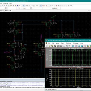
An Ultra-Low Leakage and Wide-Range Voltage Level Shifter for Low-Power Digital CMOS VLSIs
Base Paper Abstract:
This brief presents an ultra-low leakage and fast conversion level shifter with wide-range voltage conversion and frequency. The proposed level shifter adopts the leakage shutoff transistors, which can completely cut off the static current when the circuits stand by. The pull-down network employs the low-threshold transistor for the fast fall transition. The proposed level shifter also solves the swing problem and achieves a fast conversion by using the voltage hysteresis transistor, strengthening the pull-up network to ensure the internal node is fast and fully charged. Measurement results based on the 55 nm process show that the average ultra-low leakage of the proposed level shifter is 34.8 pW when converting from 0.3 V input to 1.2 V output. Meanwhile, the average propagation delay and the average energy per transition of the proposed level shifter are 13.86 ns and 22.71 fJ for an input frequency of 1 MHz, respectively. The maximum conversion range is from 0.13 V to 1.2 V. Index Terms: Level shifter, ultra-low power, multi-supply voltage circuit, sub-threshold operation.
List of the following materials will be included with the Downloaded Backup:
Analysis, Comparison, and Experimental Validation of a Class AB Voltage Follower With Enhanced Bandwidth and Slew Rate
Abstract:
This paper describes a bandwidth (BW)- and slew rate (SR)-enhanced class AB voltage follower (VF). A thorough small signal analysis of the proposed and a state-of-the-art AB-enhanced VF is presented to compare their performance. The proposed circuit has 50-MHz BW, 19.5-V/µs SR, and a BW figure of merit of 41.6 (MHz × pF/µW) for CL = 50 pF. It provides 13 times higher current efficiency and 15 times higher BW than the conventional VF with equal 60-µW static power dissipation. The experimental and simulation results of a fabricated test chip in the 130-nm CMOS technology validate the proposed circuit.
List of the following materials will be included with the Downloaded Backup: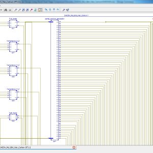
Approximate Multiplier Design Using Novel Dual-Stage 4 : 2 Compressors
Base Paper Abstract:
High speed multimedia applications have paved way for a whole new area in high speed error-tolerant circuits with approximate computing. These applications deliver high performance at the cost of reduction in accuracy. Furthermore, such implementations reduce the complexity of the system architecture, delay and power consumption. This paper explores and proposes the design and analysis of two approximate compressors with reduced area, delay and power with comparable accuracy when compared with the existing architectures. The proposed designs are implemented using 45 nm CMOS technology and efficiency of the proposed designs have been extensively verified and projected on scales of area, delay, power, Power Delay Product (PDP), Error Rate (ER), Error Distance (ED), and Accurate Output Count (AOC). The proposed approximate 4 : 2 compressor shows 56.80% reduction in area, 57.20% reduction in power, and 73.30% reduction in delay compared to an accurate 4 : 2 compressor. The proposed compressors are utilised to implement 8 × 8 and 16 × 16 Dadda multipliers. These multipliers have comparable accuracy when compared with state-of-the-art approximate multipliers. The analysis is further extended to project the application of the proposed design in error resilient applications like image smoothing and multiplication.
List of the following materials will be included with the Downloaded Backup: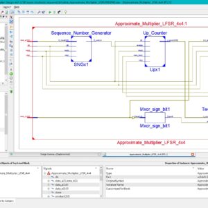
Approximate Multiplier Design with LFSR-Based Stochastic Sequence Generators for Edge AI
Base Paper Abstract:
This letter introduces an innovative approximate multiplier (AM) architecture that leverages stochastically generated bit streams through the Linear Feedback Shift Register (LFSR). The AM is applied to matrix-vector multiplication (MVM) in Neural Networks (NNs). The hardware implementations in 90 nm CMOS technology demonstrate superior power and area efficiency compared to state-of-the-art designs. Additionally, the study explores applying stochastic computing to LSTM NNs, showcasing improved energy efficiency and speed.
List of the following materials will be included with the Downloaded Backup: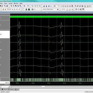
Approximate Pruned and Truncated Haar Discrete Wavelet Transform VLSI Hardware for Energy-Efficient ECG Signal Processing
Abstract:
The approximate computing paradigm emerged as a key alternative for trading off accuracy and energy efficiency. Error-tolerant applications, such as multimedia and signal processing, can process the information with lower-than-standard accuracy at the circuit level while still fulfilling a good and acceptable service quality at the application level. The automatic detection of R-peaks in an electrocardiogram (ECG) signal is the essential step preceding ECG processing and analysis. The Haar discrete wavelet transform (HDWT) is a low-complexity pre-processing filter suitable to detect ECG R-peaks in embedded systems like wearable devices, which are incredibly energy constrained. This work presents an approximate HDWT hardware architecture for ECG processing at very high energy efficiency. Our best-proposal employing pruning within the approximate HDWT hardware architecture requires just seven additions. The use of a truncation technique to improve energy efficiency is also investigated herein by observing the evolution of the signal-to-noise ratio and the ultimate impact in the ECG peak-detection application. This research finds that our HDWT approximate hardware architecture proposal accepts higher truncation levels than the original HDWT. In summary: Our results show about 9 times energy reduction when combining our HDWT matrix approximation proposal with the pruning and the highest acceptable level of truncation while still maintaining the R-peak detection performance accuracy of 99.68% on average.
List of the following materials will be included with the Downloaded Backup: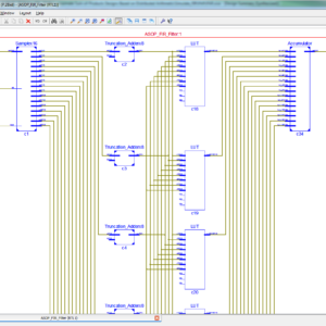
Approximate Sum-of-Products Design Based on Distributed Arithmetic
Proposed Abstract:
Approximate circuits provide high performance and require low power. Sum-of-products (SOP) units are key elements in many digital signal processing applications. In this brief, three approximate SOP (ASOP) models which are based on the distributed arithmetic are proposed. They are designed for different levels of accuracy. First model of ASOP achieves an improvement up to 64% on area and 70% on power, when compared with conventional unit. Other two models provide an improvement of 32% and 48% on area and 54% and 58% on power, respectively, with a reduced error rate compared with the first model. Third model achieves the mean relative error and normalized error distance as low as 0.05% and 0.009%, respectively. Performance of approximate units is evaluated with a noisy image smoothing application, where the proposed models are capable of achieving higher peak signal to-noise ratio than the existing state-of-the-art techniques. It is shown that the proposed approximate models achieve higher processing accuracy than existing works but with significant improvements in power and performance.
List of the following materials will be included with the Downloaded Backup: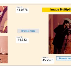
Area and Power Efficient Truncated Booth Multipliers Using Approximate Carry-Based Error Compensation
Base Paper Abstract:
Approximate computing is a promising technique to elevate the performance of digital circuits at the cost of reduced accuracy in numerous error-resilient applications. Multipliers play a key role in many of these applications. In this brief, we propose a truncation based Booth multiplier with a compensation circuit generated by selective modifications in k-map to circumvent the carry appearing from the truncated part. By judicious mapping, hardware pruning and output error reduction is achieved simultaneously. In the quest of power and accuracy trade-off, Truncated and Approximate Carry based Booth Multipliers (TACBM) are proposed with a range of designs based on truncation factor w. When compared with the state-of-the-art multipliers, TACBM outperforms in terms of accuracy and Area Power savings. TACBM (w = 10) provides with 0.02% MRED and 23% reduction in Area-Power product compared to exact Booth multiplier. The multipliers are evaluated using image blending and Multilayer perceptron (MLP) neural network and a high value of accuracy (95.63%) for MLP is achieved.
List of the following materials will be included with the Downloaded Backup:
Area Delay and Energy Efficient Multi-Operand Binary Tree Adder
Abstract:
Here, the critical path of ripple carry adder (RCA)-based binary tree adder (BTA) is analyzed to find the possibilities for delay minimization. Based on the findings of the analysis, the new logic formulation and the corresponding design of RCA are proposed for the BTA. The comparison result shows that the proposed RCA design offers better efficiency in terms of area, delay and energy than the existing RCA. Using this RCA design, the BTA structure is proposed. The synthesis result reveals that the proposed 32-operand BTA provides the saving of 22.5% in area–delay product and 28.7% in energy–delay product over the recent Wallace tree adder which is the best among available multi-operand adders. The authors have also applied the proposed BTA in the recent multiplier designs to evaluate its performance. The synthesis result shows that the performance of multiplier designs improved significantly due to the use of proposed BTA. Therefore, the proposed BTA design can be a better choice to develop the area, delay and energy efficient digital systems for signal and image processing applications.
List of the following materials will be included with the Downloaded Backup:
Area Delay Power Efficient Carry Select Adder
Source : VHDL
Abstract:
We are briefly discussing the logic operations are involved in the CSLA (conventional carry select adder) and the square root conventional carry select adder. We have discard the all the extra logic operations present in the conventional CSLA. In the proposed system carry selection is take place in before the final sum calculation. The proposed system achieves the optimization in the logic units. Finally the FPGA synthesis results shows to achieves a design the low power architecture for CSLA.
List of the following materials will be included with the Downloaded Backup:
Provide Wordlwide Online Support
We can provide Online Support Wordlwide, with proper execution, explanation and additionally provide explanation video file for execution and explanations.
24/7 Support Center
NXFEE, will Provide on 24x7 Online Support, You can call or text at +91 9789443203, or email us nxfee.innovation@gmail.com
Terms & Conditions:
Customer are advice to watch the project video file output, and before the payment to test the requirement, correction will be applicable.
After payment, if any correction in the Project is accepted, but requirement changes is applicable with updated charges based upon the requirement.
After payment the student having doubts, correction, software error, hardware errors, coding doubts are accepted.
Online support will not be given more than 3 times.
On first time explanation we can provide completely with video file support, other 2 we can provide doubt clarifications only.
If any Issue on Software license / System Error we can support and rectify that within end of day.
Extra Charges For duplicate bill copy. Bill must be paid in full, No part payment will be accepted.
After payment, to must send the payment receipt to our email id.
Powered by NXFEE INNOVATION, Pondicherry.
Call us today at : +91 9789443203 or Email us at nxfee.innovation@gmail.com
NXFEE Development & Services

Copyright © 2026 Nxfee Innovation.