Area-Efficient Bidirectional Shift-Register Using Bidirectional Pulsed-Latches
Abstract:
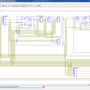
This paper proposes an area-efficient bidirectional shift-register using bidirectional pulsed-latches. The proposed bidirectional shift-register reduces the area and power consumption by replacing master-slave flip-flops and 2-to-1 multiplexers with the proposed bidirectional pulsed-latches and non-overlap delayed pulsed clock signals, and by using sub shift-registers and extra temporary storage latches. A 256-bit bidirectional shift-register was fabricated using a 65nm CMOS process. Its area was 1,943μm2 and its power consumption is 200μW at a 100MHz clock frequency with VDD=1.2V. It reduces area by 39.2% and power consumption by 19.4% compared to the conventional bidirectional shift-register, length in most cases.
List of the following materials will be included with the Downloaded Backup: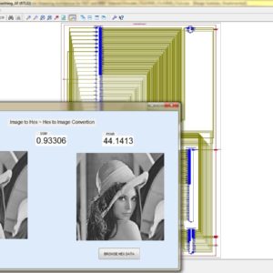
Area-Time Efficient Streaming Architecture for FAST and BRIEF Detector
Abstract:
The combination of FAST corners and BRIEF descriptors provide highly robust image features. We present a novel detector for computing the FAST-BRIEF features from streaming images. To reduce the complexity of the BRIEF descriptor, we employ an optimized adder tree to perform summation by accumulation on streaming pixels for the smoothing operation. Since the window buffer used in existing designs for computing the BRIEF point-pairs are often poorly utilized, we propose an efficient sampling scheme that exploits register reuse to minimize the number of registers. Synthesis results based on 65- nm CMOS technology show that the proposed FAST-BRIEF core achieves over 40% reduction in area-delay product compared to the baseline design. In addition, we show that the proposed architecture can achieve 1.4x higher throughput than the baseline architecture with slightly lower energy consumption.
List of the following materials will be included with the Downloaded Backup: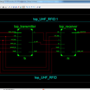
ASIC design of UHF RFID reader digital baseband
This paper presents the ASIC design and implementation of digital baseband system for UHF RFID reader based on EPC Global C1G2 /ISO 18000-6c protocol. The digital baseband system consists of two parts :transmitter and receiver, which including encoding module, decoding module, channel filers, CRC check module, control module and a SPI module. It is described in verilog HDL in RTL level, with Design Complier for synthesizing, PT for static timing analyzing and Astro for physical design. The die is fabricated using IBM 130nm 8-layer-metal RF CMOS process successfully, which size is 3 mm x 3mm, the power consumption is around 6.7mW. It can be applied in the research of single-chip UHF RFID reader. The proposed architecture of this paper analysis the logic size, area and power consumption using Xilinx 14.2.
List of the following materials will be included with the Downloaded Backup:
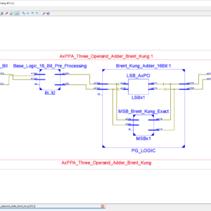
AxPPA: Approximate Parallel Prefix Adders
Base Paper Abstract:
Addition units are widely used in many computational kernels of several error-tolerant applications such as machine learning and signal, image, and video processing. Besides their use as stand-alone, additions are essential building blocks for other math operations such as subtraction, comparison, multiplication, squaring, and division. The parallel prefix adders (PPAs) is among the fastest adders. It represents a parallel prefix graph consisting of the carry operator nodes, called prefix operators (POs). The PPAs, in particular, are among the fastest adders because they optimize the parallelization of the carry generation (G) and propagation (P). In this work, we introduce approximate PPAs (AxPPAs) by exploiting approximations in the POs. To evaluate our proposal for approximate POs (AxPOs), we generate the following AxPPAs, consisting of a set of four PPAs: approximate Brent–Kung (AxPPA-BK), approximate Kogge–Stone (AxPPAKS), Ladner-Fischer (AxPPA-LF), and Sklansky (AxPPA-SK). We compare four AxPPA architectures with energy-efficient approximate adders (AxAs) [i.e., Copy, error-tolerant adder I (ETAI), lower-part OR adder (LOA), and Truncation (trunc)]. We tested them generically in stand-alone cases and embedded them in two important signal processing application kernels: a sum of squared differences (SSDs) video accelerator and a finite impulse response (FIR) filter kernel. The AxPPA-LF provides a new Pareto front in both energy-quality and area-quality results compared to state-of-the-art energy-efficient AxAs.
List of the following materials will be included with the Downloaded Backup: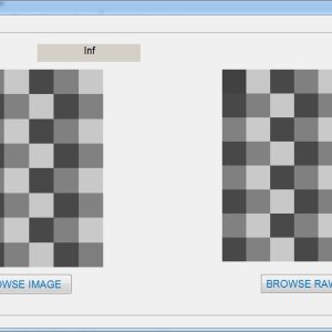
Block Interleaver Design for High Data Rate Wireless Networks
With increasing data rates in wireless communication, quality of service (QoS) has become a major issue. This is more with fading channels transmitting huge volumes of data. QoS is degraded by inter-symbol interference (ISI) and related errors. One of the simplest and convenient techniques to overcome such errors is interleaving, which is used efficiently in wireless applications. It has found applications for combating burst errors that creeps up in the channel during transmission. In this paper, an efficient model of a block interleaver using a hardware description language (Verilog) is proposed. The proposed technique reduces consumption of FPGA resources to a large extent, which implies low power consumption. The proposed architecture of this paper analysis the logic size, area and power consumption using Xilinx 14.2.
List of the following materials will be included with the Downloaded Backup:
Byte-Reconfigurable LDPC Codec Design With Application to High-Performance ECC of NAND Flash Memory Systems
Abstract: In information theory, a low-density parity-check (LDPC) code is a linear error correcting code, a method of transmitting a message over a noisy transmission channel. An LDPC is constructed using a sparse bipartite graph. LDPC codes are capacity-approaching codes, which means that practical constructions exist that allow the noise threshold to be set very close (or even arbitrarily close on the BEC) to the theoretical maximum (the Shannon limit) for a symmetric memory-less channel. The noise threshold defines an upper bound for the channel noise, up to which the probability of lost information can be made as small as desired. Using iterative belief propagation techniques, LDPC codes can be decoded in time linear to their block length.
List of the following materials will be included with the Downloaded Backup:
Camouflaged Logic Gates Using Threshold-Voltage-Defined Memory Cells
This brief proposes two types of camouflaged logic gates using threshold-voltage-defined memory cells (TVD-MCs). The proposed multiplexer-select TVD-MC (MS-TVDMC) gate consists of a target logic gate, several camouflage logic gates, a multiplexer (MUX), and TVD-MCs. All logic gates and MUX are implemented with standard threshold-voltage transistors. The TVD-MC is composed of two cross coupled inverters with low- or high-threshold-voltage transistors. When its supply voltage increases from ground to VDD, its data become “0” or “1” according to the threshold voltages of transistors in two inverters. The target logic gate is selected with the MUX by the data stored in the TVD-MCs. The data are defined by the threshold voltages of transistors, so that it is difficult to distinguish the target logic gate from the other camouflage logic gates. The proposed logic-merged TVD-MC (LM-TVDMC) gate merges all logic gates and MUX in the MS-TVDMC gate at the transistor level. The proposed camouflaged gates significantly reduce the delay, power consumption, and leakage current compared to the conventional dynamic enhanced-TVD (DE-TVD) camouflaged gate requiring the dynamic power and delay overheads and the conventional threshold-voltage-defined (TVD) switch camouflaged gate with large ON-resistances in switch transistors. Index Terms: Camouflaged gate, logic gate, reverse engineering, security, threshold-voltage-defined (TVD).
List of the following materials will be included with the Downloaded Backup:
Chaos-Based Bitwise Dynamical Pseudorandom Number Generator on FPGA
Abstract:
In this paper, a new pseudorandom number generator (PRNG) based on the logistic map has been proposed. To prevent the system to fall into short period orbits as well as increasing the randomness of the generated sequences, the proposed algorithm dynamically changes the parameters of the chaotic system. This PRNG has been implemented in a vertex 7 field-programmable gate array (FPGA) with a 32-bit fixed point precision, using a total of 510 lookup tables (LUTs) and 120 registers. The sequences generated by the proposed algorithm have been subjected to the National Institute of Standards and Technology (NIST) randomness tests, passing all of them. By comparing the randomness with the sequences generated by a raw 32-bit logistic map, it is shown that, by using only an additional 16% of LUTs, the proposed PRNG obtains a much better performance in terms of randomness, increasing the NIST passing rate from 0.252 to 0.989. Finally, the proposed bitwise dynamical PRNG is compared with other chaos-based realizations previously proposed, showing great improvement in terms of resources and randomness.
List of the following materials will be included with the Downloaded Backup:
CMOS First-Order All-Pass Filter With 2-Hz Pole Frequency
Abstract:
A CMOS fully integrated all-pass filter with an extremely low pole frequency of 2 Hz is introduced in this paper. It has 0.08-dB passband ripple and 0.029-mm2Si area. It has 0.38-mW power consumption in strong inversion with ±0.6-V power supplies. In subthreshold, it has 0.64-µW quiescent power and operates with ±200-mV dc supplies. Miller multiplication is used to obtain a large equivalent capacitor without excessive Si area. By varying the gain of the Miller amplifier, the pole frequency can be varied from 2 to 48 Hz. Experimental and simulation results of a test chip prototype in 130-nm CMOS technology validate the proposed circuit.
List of the following materials will be included with the Downloaded Backup:
Column-Selection-Enabled 10T SRAM Utilizing Shared Diff-VDD Write and Dropped-VDD Read for Power Reduction
Abstract:
A non-destructive column-selection-enabled 10T SRAM for aggressive power reduction is presented in this brief. It frees a half-selected behavior by exploiting the bit line-shared data-aware write scheme. The differential-VDD (Diff-VDD) technique is adopted to improve the write ability of the design. In addition, its decoupled read bit lines are given permission to be charged and discharged depending on the stored data bits. In combination with the proposed dropped-VDD biasing, it achieves the significant power reduction. The experimental results show that the proposed design provides the 3.3× improvement in the write margin compared with the standard Diff-10T SRAM. A 5.5-kb 10T SRAM in a 65-nm CMOS process has a total power of 51.25 µW and a leakage power of 41.8 µW when operating at 6.25 MHz at 0.5 V, achieving 56.3% reduction in dynamic power and 32.1% reduction in leakage power compared with the previous single-ended 10T SRAM.
List of the following materials will be included with the Downloaded Backup:
Combating Data Leakage Trojans in Commercial and ASIC Applications With Time-Division Multiplexing and Random Encoding
Proposed Abstract:
This paper explains the concept of reduction of data leakage Trajons in modulation scheme of TDM (Time Division Multiplexing) using DES (Data Encryption Standard) encoding and decoding concept. The DES is a symmetric key block cipher which is used for encryption and decryption process. In hardware manufacturing, detection and prevention of hardware Trajons attacks becomes a major concern for a manufacturing company. Because, the hardware Trajons is able to steal some sensitive information of a users such as encryption keys, passwords, etc,. So, most defensive methods prefers on prevention of data. The existing system uses the concept of RECORD ( Randomized encoding of combinational logic for resistance to data leakage) to prevent the data from the hardware Trajons even the Trajons known the entire information. Thus the proposed system of TDM version of RECORD design is more secure than the Sequential RECORD system and these case of existing work, will not concentrate and proved TDM RECORD DES Decryption Algorithm. Therefore, the proposed work of this paper will used the concept of TDM version using RECORD with implement in Encryption and Decryption Algorithm and also BER Testing, this method will have designed in Verilog HDL and implement in Xilinx FPGA and finally shown the comparison results in terms of area, delay and power.
List of the following materials will be included with the Downloaded Backup:
Comparative study of 16-order FIR filter design using different multiplication techniques
Abstract:
This study represents designing and implementation of a low power and high speed 16 order FIR filter. To optimize filter area, delay and power, different multiplication techniques such as Vedic multiplier, add and shift method and Wallace tree (WT) multiplier are used for the multiplication of filter coefficient with filter input. Various adders such as ripple carry adder, Kogge Stone adder, Brent Kung adder, Ladner Fischer adder and Han Carlson adder are analyzed for optimum performance study for further use in various multiplication techniques along with barrel shifter. Secondly optimization of filter area and delay is done by using add and shift method for multiplication, although it increases power dissipation of the filter. To reduce the complexity of filter, coefficients are represented in canonical signed digit representation as it is more efficient than traditional binary representation. The finite impulse-response (FIR) filter is designed in MATLAB using equiripple method and the same filter is synthesized on Xilinx Spartan 3E XC3S500E target field-programmable gate array device using Very High Speed Integrated Circuit Hardware Description Language (VHDL) subsequently the total on-chip power is calculated in Vivado2014.4. The comparison of simulation results of all the filters show that FIR filter with WT multiplier is the best optimized filter.
List of the following materials will be included with the Downloaded Backup:
Comparison and Extension of Approximate 4-2 Compressors for Low-Power Approximate Multipliers
Abstract:
Approximate multipliers attract a large interest in the scientific literature that proposes several circuits built with approximate 4-2 compressors. Due to the large number of proposed solutions, the designer who wishes to use an approximate 4-2 compressor is faced with the problem of selecting the right topology. In this paper, we present a comprehensive survey and comparison of approximate 4-2 compressors previously proposed in literature. We present also a novel approximate compressor, so that a total of twelve different approximate 4-2 compressors are analyzed. The investigated circuits are employed to design 8 × 8 and 16 × 16 multipliers, implemented in 28nm CMOS technology. For each operand size we analyze two multiplier configurations, with different levels of approximations, both signed and unsigned. Our study highlights that there is no unique winning approximate compressor topology since the best solution depends on the required precision, on the signedness of the multiplier and on the considered error metric.
List of the following materials will be included with the Downloaded Backup:
Concept Design and Implementation of Reconfigurable CORDIC
This brief presents the key concept, design strategy, and implementation of reconfigurable coordinate rotation digital computer (CORDIC) architectures that can be configured to operate either for circular or for hyperbolic trajectories in rotation as well as vectoring-modes. It can, therefore, be used to perform all the functions of both circular and hyperbolic CORDIC. We propose three reconfigurable CORDIC designs: 1) a reconfigurable rotation-mode CORDIC that operates either for circular or for hyperbolic trajectory; 2) a reconfigurable vectoring-mode CORDIC for circular and hyperbolic trajectories; and 3) a generalized reconfigurable CORDIC that can operate in any of the modes for both circular and hyperbolic trajectories. The reconfigurable CORDIC can perform the computation of various trigonometric and exponential functions, logarithms, square-root, and so on of circular and hyperbolic CORDIC using either rotation-mode or vectoring-mode CORDIC in one single circuit. It can be used in digital synchronizers, graphics processors, scientific calculators, and so on. It offers substantial saving of area complexity over the conventional design for reconfigurable applications. The proposed architecture of this paper analysis the logic size, area and power consumption using Xilinx 14.2.
List of the following materials will be included with the Downloaded Backup:
Constant Time Hardware Architecture for a Gaussian Smoothing Filter
Abstract:
In this paper a new and highly efficient hardware architecture for a bit-serial implementation of a 3*3 filter on FPGA is developed and presented. The concept is implemented on a Gaussian blur spatial filter and it can be extended to other filters with similar characteristics. The proposed Single Instruction Multiple Data (SIMD) architecture provides a constant operating time independent of the size of the given image while the arithmetic operations are limited to the operations of addition. The Multiple Instruction Multiple Data (MIMD) performance is achieved in a near fraction of the cost. Thus, the hardware’s utilization is optimized. The total time needed to perform the filter of interest on the given image is solely dependent on the working clock frequency. The proposed design is evaluated using a small image and is implemented on two FPGA families with various sizes of an image. Also, it is compared with other architectures.
List of the following materials will be included with the Downloaded Backup:
Design and Analysis of a Majority Logic Based Imprecise 6-2 Compressor for Approximate Multipliers
Base Paper Abstract:
Approximate computing is an emerging paradigm for trading off computing accuracy to reduce energy consumption and design complexity in a variety of applications, for which exact computation is not a critical requirement. Different from conventional designs using AND-OR and XOR gates, the majority gate is widely used in many emerging nanotechnologies. An ultra-efficient 6-2 compressor is proposed in this paper. It is composed of two majority gates that lead to low energy consumption and high hardware efficiency. The proposed compressor is utilized in the approximate partial product reduction of a modified 8×8 Dadda multiplier with a truncated structure. Experimental results show that this multiplier realizes a significant reduction in hardware cost, especially in terms of power and area, on average by up to 40% and 31% respectively, compared to exact and state-of-the-art designs. The application of image multiplication is also presented to assess the practicability of the multiplier. The results show that the proposed multiplier results in images with higher quality in peak signal to noise ratio (PSNR) and mean structural similarity index metric (MSSIM) compared to other designs.
List of the following materials will be included with the Downloaded Backup:
Design and Analysis of Approximate Compressors for Multiplication
Inexact computing is particularly interesting for computer arithmetic designs. Implementation of 8X8 truncated multipliers using Very High Speed Integrated Circuit Hardware Description Language (VHDL). Truncated multipliers can be used in the image multiplication application. This multiplier is automatically truncating the output and reduces the power consumption and are comparing to other multipliers. The proposed architecture of this paper analysis the logic size, area and power consumption using Xilinx 14.2.
List of the following materials will be included with the Downloaded Backup:
Design and Analysis of Energy Efficient Approximate Multipliers for Image Processing and DNN
Base Paper Abstract:
Numerous obstacles in enhancing the performance of computing systems have spurred the emergence of approximate computing. Extensive studies have been reported on approximate computing to develop high-performance, energy-efficient hardware designs tailored to error-resilient applications. In this brief, we proposed 8-bit approximate multipliers with 15 levels of accuracy using three techniques: recursive, bit-wise, and hybrid approximation using partial bit OR (PBO). Compared to the existing multipliers, investigated designs have significantly improved the area, power, delay, Power Delay Product (PDP), and Power Area Delay Product (PADP) by 41.68%, 73.16%, 35.57%, 72.65%, and 75.42% respectively on average. On resemblance with the accurate multiplier, the area, power, delay, PDP, and PADP were enhanced by 54.41%, 57.57%, 25.73%, 60.14%, and 74.33% correspondingly on average. Peak Signal-to-Noise Ratio (PSNR) and Structural Similarity Index Measure (SSIM) values surpassing (30 dB, 94%), (31 dB, 96%), and (26 dB, 95%) by applying them to benchmarks in image smoothing, edge detection, and image sharpening successively. Moreover, upon scrutinizing the efficacy of multipliers in hardware implementations of deep neural networks attaining the performance exceeding 95%. The obtained results confirm that suggested multipliers are well-suited for their widespread applications.
List of the following materials will be included with the Downloaded Backup: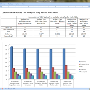
Design and analysis of High speed Wallace tree multiplier using parallel prefix adders for VLSI circuit designs
Abstract:
Major operation block in any processing unit is a multiplier. There are many multiplication algorithms are proposed, by using which multiplier structure can be designed. Among various multiplication algorithms, Wallace tree multiplication algorithm is beneficial in terms of speed of operation. With the advancement of technology, demand for circuits with high speed and low area is increasing. In order to improve the speed of Wallace tree multiplier without degrading its area parameter, a new structure of Wallace tree multiplier is proposed in this paper. In the proposed structure, the final addition stage of partial products is performed by parallel prefix adders (PPAs). In this paper, five Wallace tree multiplier structures are proposed using Kogge stone adder, Sklansky adder, Brent Kung adder, Ladner Fischer adder and Han carlson adder. All the multiplier structures are designed using Verilog HDL in Xilinix 13.2 design suite. The proposed structures are simulated using ISIM simulator and synthesized using XST synthesizer. The proposed designs are analyzed with respect to traditional multiplier design in terms of area (No. of LUTs) and delay (ns).
List of the following materials will be included with the Downloaded Backup:
Design and analysis of Reversible Approximate Full Adder and its applications with Optimized 4:2, 5:2, 7:2 Compressors for Efficient Approximate Multipliers
Design and Application of Mean and Square Root Circuits for Stochastic Computing
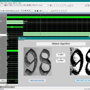
Stochastic computing (SC) is an unconventional computing paradigm that represents values using probabilities. This representation enables simple logic gates to perform complex arithmetic operations. This brief proposes two low hardware-cost stochastic mean circuits for even and odd inputs, respectively, along with a high-accuracy stochastic square root circuit. The circuits are designed by considering correlation technique and achieve excellent performance. Experimental results demonstrate that the proposed mean circuits surpass previous counterparts in computing accuracy and hardware cost. For instance, the proposed 9-input mean circuit can achieve at least an 86.7% reduction in mean square error (MSE) and a 28.6% reduction in area. For the square root circuit, the proposed design achieves a reduction in MSE of at least 19.6%. The proposed circuits are further demonstrated with the Niblack binarization algorithm, which shows superior performance of accuracy. Index Terms: Stochastic computing, mean circuit, square root circuit, binarization processing.
List of the following materials will be included with the Downloaded Backup:
Design and Development of OFDM Baseband Transceiver using VIRTEX 6 FPGA Family
Broadband Wireless Access (BWA) is a successful technology which offers high speed voice, internet connection and video. One of the leading candidates for Broadband Wireless Access is Wi-MAX; it is a technology that compiles with the IEEE 802.16 family of standards. This paper mainly focused towards the hardware Implementation of Wireless MAN-OFDM Physical Layer of IEEE Std 802.16d Baseband Transceiver on FPGA. The RTL coding of VHDL was used, which provides a high level design-flow for developing and validating the communication system protocols and it provides flexibility of changes in future in order to meet real world performance evaluation. This proposed system is analysis area and power. Also the outputs are verified using Xilinx 14.2.
List of the following materials will be included with the Downloaded Backup:
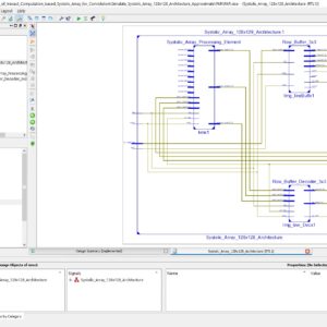
Design and Evaluation of Inexact Computation based Systolic Array for Convolution
Base Paper Abstract:
Systolic Array (SA) architecture is a unique computation architecture where the inputs are continuously flowing, and the processing elements perform the desired computations in parallel. SA’s are prominently investigated due to the emergence of heavy and large processing elements for modern-day Convolution Neural Network (CNN) applications. Taking this cue, SA architectures of the order of kernel size and configured with approximate multipliers are investigated for image processing applications. The approximate array multiplier derived from approximate 4-2 compressors were employed to achieve hardware benefits without losing on the image quality metrics. The SA architecture is configured to the same size as filter kernels in a view to achieve maximum utilization, and the same is compared with other existing SA architectures for hardware metrics. The computational time for processing an image of size 256 × 256 was evaluated for approximated SA. This work investigates approximate SA for Gaussian smoothing and image outline feature extraction applications to showcase the reliability of the design. The novel approximate SA architecture is a step toward designing compact sized SoC designs for real-time image and video processing applications.
List of the following materials will be included with the Downloaded Backup:
Design and FPGA Implementation of Lattice Wave Digital Notch Filter with Minimal Transient Duration
Abstract:
In this study, the design and field-programmable gate array (FPGA) implementation of the digital notch filter with the lattice wave digital filter (LWDF) structure is presented. For reducing the initial signal transient, the variable notch bandwidth filter is designed. During the initial samples, the notch filter has a wide bandwidth in order to diminish signal transient. As time moves forward, the notch bandwidth reduces to attain the possible minimum width. This results in minimized transient duration notch filter with a sufficiently high-quality factor. Previously, the IIR structure has been used for implementing the time varying bandwidth notch filter. Such a filter requires two variable coefficients for varying the notch width with time. The advantage of using a LWDF structure is that only one coefficient has variable values to vary the notch width with time. Therefore, the number of memory locations required to implement the proposed design is reduced by half. Moreover, the LWDF is less sensitive to the word-length effects. Thus, the proposed lattice wave digital notch filter (LWDNF) produces better results compared to the existing literature in terms of error analysis. The suggested LWDNF is then implemented on a field-programmable gate array using a Xilinx system generator for the DSP design suite.
List of the following materials will be included with the Downloaded Backup:
Design and Implementation of 32-bit CSPRNG using the PRESENT cipher with Dual Polynomial PRNG for Enhanced Randomness and Precision
Base Paper Abstract:
Random Number Generators (RNGs) are substantially used in many security domains, providing a fundamental source of unpredictability essential for tasks such as cryptography, simulations, and statistical analyses. The efficiency and quality of an RNG directly impact the reliability and security of diverse applications, making advancements in RNG design, as explored in this study, of significant importance for enhancing computational processes. This paper presents an innovative Pseudo-Random Number Generator (PRNG) that leverages the efficiency of two carefully selected Linear Feedback Shift Registers (LFSRs) and a connecting XOR gate. The investigation of five polynomials identified an optimal pair, resulting in a notable improvement of over 200X in the length of random bit sequences compared to a single LFSR-based PRNG. The Basys3 FPGA board with the xc7a35tcpg236-1 FPGA chip was used to implement and synthesize the proposed design. Two significant findings emerge from this research. Firstly, using variable polynomials demonstrates a huge enhancement in the duration of randomness, outperforming the impact of variable seeds. A noteworthy observation is that employing the same polynomials in different branches does not result in optimal results. Secondly, managing more seeds is associated with an increased area cost, underscoring the efficiency of handling two polynomials.
List of the following materials will be included with the Downloaded Backup:
Design and Implementation of a Low-Complexity Continuously Variable Digital Filter
Base Paper Abstract:
Variable filters with adjustable bandwidth are vital components in diverse communication scenarios. This paper presents an innovative architecture for a continuously variable bandwidth filter using a fixed hardware. Our approach integrates a fixed finite impulse response filter between two arbitrary fractional delay filters implemented through a novel Farrow Equivalent-Newton structure. The proposed architecture provides a low-complexity implementation structure compared to the state-of-the-art approaches. A precise mapping equation for the edge frequencies of the filters generated from the proposed continuously variable bandwidth filter, in terms of a variable parameter called the resampling ratio, is also formulated. Validation experiments encompass the design of continuously variable bandwidth filters tailored to various wireless communication standards. The hardware utilisation report of the proposed continuously variable bandwidth filter obtained by synthesising the structure using Xilinx Vivado 2020.2 on a Kintex-7 device is also included, which proves the hardware complexity reduction and efficiency of the proposed structure.
List of the following materials will be included with the Downloaded Backup:
Design and Implementation of a Unified Digital Clock and Stopwatch System Using FSM and Multiplexed Seven-Segment Display
Proposed Abstract:
Digital clocks and stopwatches are widely used in daily applications such as consumer electronics, embedded devices, portable medical instruments, and time monitoring systems, as they provide simple and accurate time tracking functions. These systems offer advantages like low cost, user-friendly operation, and high reliability; however, they often face disadvantages such as hardware redundancy, higher power consumption, and limited integration when clock and stopwatch functions are implemented separately. The main problem addressed in this work is the lack of a unified architecture that can perform both digital clock and stopwatch operations using shared resources, which leads to inefficient hardware utilization and increased complexity in existing designs. Conventional systems generally use independent controllers and dedicated display drivers, resulting in additional overhead. To overcome this limitation, we propose a finite state machine based architecture that integrates both digital clock and stopwatch modules into a single design with common display hardware. The system employs multiplexers and control signals to switch seamlessly between clock and stopwatch modes, while states such as idle, hour, minute, second, and pause are clearly managed through FSM logic. The novelty of this work lies in the resource-sharing approach where a common seven-segment display is driven by multiplexed outputs, thereby reducing area, power, and switching complexity without compromising accuracy. The proposed design is implemented and tested using hardware description language coding and simulated on FPGA-based platforms, ensuring precise timing, functional correctness, and display reliability. Performance evaluation confirms that the system achieves efficient utilization of logic resources, accurate real-time operation, and flexibility for future extension in low-power VLSI and IoT-based applications.
List of the following materials will be included with the Downloaded Backup:
Design and Implementation of an 8-bit Approximate Wallace Tree Multiplier for Energy Efficient Deep Neural Networks
Base Paper Abstract:
Approximate arithmetic computing circuits and architectures have been proven to be energy efficient designs for Deep Neural Networks (DNNs) which are error resilient. In this paper, an approximate 8-bit Wallace Multiplier has been proposed and designed in 90nm CMOS technology for energy efficiency. The proposed 8-bit approximate multiplier design consumes ~32% less energy in comparison to an accurate 8-bit Wallace Tree multiplier with less than 20% Mean Relative Error (MRE).
List of the following materials will be included with the Downloaded Backup:
Design and Implementation of Arithmetic Logic Unit in DSCH3 and Microwind
Proposed Abstract:
The Arithmetic Logic Unit (ALU) is a fundamental component in digital systems, particularly in the central processing units (CPUs) of microprocessors, where it executes essential arithmetic and logical functions. This paper presents the design and implementation of an 8-bit Arithmetic Logic Unit (ALU) using CMOS technology, developed and simulated in DSCH3 and Microwind environments. The primary goal of this research is to design an efficient and compact ALU optimized for performance and area efficiency. The 8-bit ALU performs eight operations: ripple carry addition, ripple borrow subtraction, multiplication, XOR, left shift, right shift, NAND, and NOR. Each logic gate within the ALU is constructed using CMOS logic to enhance power efficiency and integration density. This paper provides a detailed description of the ALU's CMOS-based architecture, its key components, and the control mechanism for operation selection. Performance metrics, including speed, area efficiency, and power consumption, are analyzed to assess the ALU’s effectiveness in CMOS technology.
List of the following materials will be included with the Downloaded Backup:
Design and Implementation of Arithmetic Logic Unit in HDL
Proposed Abstract:
Arithmetic logic unit (ALU) is an important part of all digital gadgets and applications. This paper presents the design and implementation of an 8-bit Arithmetic Logic Unit (ALU) with a capability to perform eight distinct operations. ALUs are fundamental components in the central processing units (CPUs) of microprocessors and are responsible for executing arithmetic and logical operations. The primary objective of this research is to design an efficient and versatile 8-bit ALU that can execute a wide range of operations while optimizing for performance and area efficiency. The proposed 8-bit ALU is designed to perform the following eight operations: Ripple carry addition, Ripple borrow subtraction, Array multiplication, XOR operation, left shift, right shift, NAND operation and a logical NOR operation. The research presents a detailed description of the ALU's architecture, its constituent components, and the control mechanism for selecting operations. Performance metrics, such as speed, area efficiency, and power consumption, are analyzed and compared with Xilinx FPGA.
List of the following materials will be included with the Downloaded Backup:
Design and Implementation of Efficient Streaming Deblocking and SAO Filter for HEVC Decoder
We have also Code for 720 x 576 Image Resolution using 64 x 64 Block Size of HEVC. Cost of this Update work in High Resolution Rs. 45,000/- ( Rs. 45,000/- + Rs. 35,000/- ) : Total Cost : Rs. 80,000/-
Abstract:
This paper aims to design an efficient mixed serial five-stage pipeline processing hardware architecture of deblocking filter (DBF) and sample adaptive offset (SAO) filter for high efficiency video coding decoder. The proposed hardware is designed to increase the throughput and reduce the number of clock cycles by processing the pixels in a stream of 4 × 36 samples in which edge filters are applied vertically in a parallel fashion for processing of luma/chroma samples. Subsequently these filtered pixels are transposed and reprocessed through vertical filter for horizontal filtering in a pipeline fashion. Finally, the filtered block transposed back to the original orientation and forwarded to a three-stage pipeline SAO filter. The proposed architecture is implemented in field programmable gate array and application specific integrated circuit platform using 90-nm library. Experimental results illustrate that the proposed DBF and SAO architecture decreases the processing cycles (172) required for processing each 64 × 64 or large coding unit compared with the state-of-the-art literature with the increase of gate count (593.32K) including memory. The results show that the throughput of the proposed filter can successfully decode ultrahigh definition video sequences at 200 frames/s at 341 MHz.
List of the following materials will be included with the Downloaded Backup:
Design and Low-Complexity Implementation of Matrix–Vector Multiplier for Iterative Methods in Communication Systems
Abstract: Iterative methods are basic building blocks of communication systems and often represent a dominating part of the system, and therefore, they necessitate careful design and implementation for optimal performance. In this brief, we propose a novel field programmable gate arrays design of matrix–vector multiplier that can be used to efficiently implement widely adopted iterative methods. The proposed design exploits the sparse structure of the matrix as well as the fact that spreading code matrices have equal magnitude entries. Implementation details and timing analysis results are promising and are shown to satisfy most modern communication system requirements.
List of the following materials will be included with the Downloaded Backup:
Design Methodology for Voltage Scaled Clock Distribution Networks
Abstract:
A low-voltage/swing clocking methodology is developed through both circuit and algorithmic innovations. The primary objective is to significantly reduce the power consumed by the clock network while maintaining the circuit performance the same. a novel D-flip-flop (DFF) cell that maximizes power savings by enabling low-voltage/swing operation throughout the entire clock network . In this proposed design of the LSFF is consume the less power compare to existing design. The proposed architecture of this paper is analysis the logic size, area and power consumption using tanner tool.
List of the following materials will be included with the Downloaded Backup: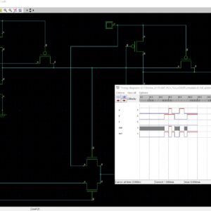
Design of 4-bit Ripple carry adder and using 9T full adder

Design of a Hardware Efficient Approximate 4-2 Compressor for Multiplication in Image Processing
Base Paper Abstract:
This letter presents a novel hardware-efficient approximate 4-2 compressor design that significantly enhances accuracy through a systematic analysis of input patterns obtained from practical applications. We incorporate a majority operation and a compound gate in the compressor design to effectively boost hardware efficiency in multiplications. Our design approach results in substantial error reductions, with normalized mean error distance (NMED) and mean relative error distance (MRED) decreasing by up to 74.84% and 82.04%, respectively, compared to existing approximate multipliers discussed in this letter. When implemented in a 32-nm CMOS technology, the approximate multiplier adopting the proposed 4-2 compressor achieves excellent hardware efficiency, reducing area, power, and energy consumption by up to 8.95%, 13.02%, and 13.02%, respectively, compared to the other alternatives. Moreover, our design delivers enhanced performance in image processing tasks, achieving up to a 4.84× increase in peak signal-to-noise ratio (PSNR) compared to other designs, all while optimizing hardware efficiency. Index Terms—Approximate multiplier, majority operation, compound gate, image processing, approximate 4-2 compressor.
List of the following materials will be included with the Downloaded Backup:
Design of a Low-Power Analog Integrated Deep Convolutional Neural Network
Base Paper Abstract:
In this article, a framework for the analog implementation of a deep convolutional neural network (CNN) is introduced and used to derive a new circuit architecture which is composed of an improved analog multiplier and circuit blocks implementing the ReLU activation function and the argmax operator. The operating principles of the individual blocks, as well as those of the complete architecture, are analysed and used to realize a low-power analog classifier, consuming less than 1.8 µW. The proper operation of the classifier is verified via a comparison with a software equivalent implementation and its performance is evaluated against existing circuit architectures. The proposed architecture is implemented in a TSMC 90-nm CMOS process and simulated using Cadence IC Suite for both schematic and layout design. Corner and Monte Carlo mismatch simulations of the schematic and the physical circuit (post layout) were conducted to evaluate the effect of transistor mismatches and process voltage temperature (PVT) variations and to showcase a proposed systematic method for offsetting their effect.
List of the following materials will be included with the Downloaded Backup:
Design of a Scalable Low Power 1 bit Hybrid Full Adder for Fast Computation
Abstract:
A novel design of a hybrid Full Adder (FA) using Pass Transistors (PTs), Transmission Gates (TGs) and Conventional Complementary Metal Oxide Semiconductor (CCMOS) logic is presented. Performance analysis of the circuit has been conducted using Cadence toolset. For comparative analysis, the performance parameters have been compared with twenty existing FA circuits. The proposed FA has also been extended up to a word length of 64 bits in order to test its scalability. Only the proposed FA and five of the existing designs have the ability to operate without utilizing buffer in intermediate stages while extended to 64 bits. According to simulation results, the proposed design demonstrates notable performance in power consumption and delay which accounted for low power delay product. Based on the simulation results, it can be stated that the proposed hybrid FA circuit is an attractive alternative in the data path design of modern high-speed Central Processing Units.
List of the following materials will be included with the Downloaded Backup:
Design of Approximate Restoring Divider
Proposed Abstract:
Approximate computing is an emerging paradigm in error-tolerant applications that leads to power-efficient designs without significant loss in quality. The divider in these applications have complex hardware and more latency among the computational blocks resulting in power consumption. Hence approximating the division module would lead to designs with vastly improved power efficiency. A new approximate subtractor (AxSUB) is proposed in this paper with the intent to reduce the hardware complexity while achieving accuracy within permissible limits. The proposed AxSUB and existing approximate subtractor units are used in the restoring array division (RAD) architecture to prove the efficacy of the AxSUB. This proposed architecture design with 8/4 approximate divider using Verilog HDL and synthesized using Xilinx Spartan 6 FPGA, and proved the performance of area, delay and power.
List of the following materials will be included with the Downloaded Backup:
Design of Area-Efficient and Highly Reliable RHBD 10T Memory Cell for Aerospace Applications
Abstract:
In this brief, based on upset physical mechanism together with reasonable transistor size, a robust 10T memory cell is first proposed to enhance the reliability level in aerospace radiation environment, while keeping the main advantages of small area, low power, and high stability. Using Taiwan Semiconductor Manufacturing Company 65-nmCMOS commercial standard process, simulations performed in Cadence Spectre demonstrate the ability of the proposed radiation-hardened-by-design 10T cell to tolerate both 0 →1and1→0 single node upsets, with the increased read/write access time.
List of the following materials will be included with the Downloaded Backup: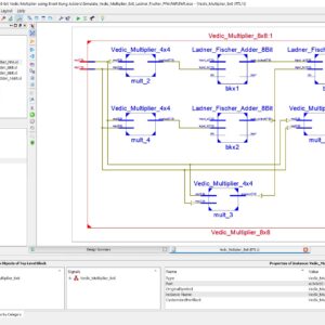
Design of High Speed 8-bit Vedic Multiplier using Brent Kung Parallel Prefix Adder
Base Paper Abstract:
One of the primary purposes of a digital signal processing system is multiplication. The multiplier’s performance affects the DSP system’s overall performance. Therefore, it is crucial to create an effective and quick multiplier implementation design. Vedic mathematics can be used to simplify complex computations so that they are easier to perform verbally. Urdhva Triyambakam is the multiplication algorithm used in Vedic math. In this paper, we employing Brent Kung adder to enhance the Vedic multiplier’s performance. The Urdhva Tiryagbhyam sutra is being used in place of other multiplication strategies since it applies to all instances of algorithms for N x N bit numbers and produces the least amount of latency. Four 4-bit vedic multipliers, two 8-bit Brent Kung adders, one 4-bit Brent Kung adder, and an OR gate are used to create an 8-bit vedic multiplier. A 4-bit vedic multiplier is created similarly by combining four 2-bit vedic multipliers, two 4-bit Brent Kung Adders, one 2-bit Brent Kung Adder, and one OR gate. These four-bit vedic multipliers are then combined to form an eight-bit vedic multiplier. After that, Xilinx Vivado Software is used to simulate and synthesis the 8 x 8 Vedic Multiplier, which was coded in Verilog HDL. The proposed Vedic Multiplier is outperformed in terms of speed when compared to related works.
List of the following materials will be included with the Downloaded Backup:
Design of Low Power High Performance 2-4 and 4-16 Mixed-Logic Line Decoders
Abstract:
This paper introduces a mixed-logic design method for line decoders, combining transmission gate logic, pass transistor dual-value logic and static CMOS. Two novel topologies are presented for the 2-4 decoders: a 14-transistor topology aiming on minimizing transistor count and power dissipation and a 15-transistor topology aiming on high power delay performance. Both a normal and an inverting decoder are implemented in each case, yielding a total of four new designs. Furthermore, four new 4-16 decoders are designed, by using mixed-logic 2-4 pre decoders combined with standard CMOS post-decoder. All proposed decoders have full swinging capability and reduced transistor count compared to their conventional CMOS counterparts. Finally, a variety of comparative spice simulations at the 32 nm shows that the proposed circuits present a significant improvement in power and delay, outperforming CMOS in almost all cases.
List of the following materials will be included with the Downloaded Backup: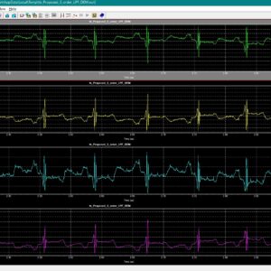
Design of Low-Power and Area Efficient ECG Low Pass Filter Using VSCP
Electrocardiogram (ECG) signal processing is a core requirement in wearable and portable healthcare systems, where long battery life, compact hardware, and reliable signal quality are increasingly demanded by modern medical applications. The aim of this work is to address the challenge of designing an energy-efficient and area-optimized ECG low-pass filter capable of suppressing high-frequency noise while preserving diagnostically important cardiac information in advanced CMOS technology. To achieve this, a low-pass filter based on a vertical source-coupled pair (VSCP) transconductance architecture is proposed, in which the circuit topology and biasing strategy are carefully optimized to suit ECG signal bandwidth and low-voltage operation. The architectural novelty of this work lies in the adaptation and refinement of a VSCP-based transconductance structure into an ECG-specific low-pass filter with reduced transistor count, improved linearity, and enhanced power efficiency in a 45-nm CMOS process. The proposed filter supports essential ECG signal conditioning functions, including low-frequency passband preservation, effective attenuation of out-of-band noise, and stable operation under low-power constraints. The design is implemented and simulated using Tanner EDA tools, and realistic ECG input signals generated from the MIT-BIH database are applied to validate functional performance. Simulation results demonstrate that the proposed filter achieves notable reductions in power consumption and silicon area compared to conventional ECG low-pass filter designs, while maintaining reliable frequency response and low noise, making it well suited for compact and battery-operated ECG monitoring systems.
List of the following materials will be included with the Downloaded Backup: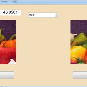
Design of Power and Area Efficient Approximate Multipliers
Abstract:
Approximate computing can decrease the design complexity with an increase in performance and power efficiency for error resilient applications. This brief deals with a new design approach for approximation of multipliers. The partial products of the multiplier are altered to introduce varying probability terms. Logic complexity of approximation is varied for the accumulation of altered partial products based on their probability. The proposed approximation is utilized in two variants of 16-bit multipliers. Synthesis results reveal that two proposed multipliers achieve power savings of 72% and 38%, respectively, compared to an exact multiplier. They have better precision when compared to existing approximate multipliers. Mean relative error figures are as low as 7.6% and 0.02% for the proposed approximate multipliers, which are better than the previous works. Performance of the proposed multipliers is evaluated with an image processing application, where one of the proposed models achieves the highest peak signal to noise ratio.
List of the following materials will be included with the Downloaded Backup:
Design of Reconfigurable Digital IF Filter with Low Complexity
Abstract:
Due to limited frequency resources, new services are being applied to the existing frequencies, and service providers are allocating some of the existing frequencies for newly enhanced mobile communications. Because of this frequency environment, repeater and base station systems for mobile communications are becoming more complicated, and frequency interference caused by multiple bands and services is getting worse. Therefore, a heterodyne receiver using IF filters with high selectivity has been used to minimize the interference between frequencies. However, repeater and base station systems in mobile communications employing fixed IF filters cannot actively cope with the usage of multiple frequency bands, the application of various services, and frequency recycling. Therefore, this brief proposes a reconfigurable digital IF filter with variable center frequency and bandwidth while achieving high selectivity as existing IF filters. The center frequency of filter can vary from 10MHz to 62.5MHz, and the filter bandwidth can be selective to one of 10MHz, 15MHz, and 20MHz. The proposed digital filter also reduces the complexity of adders and multipliers by 38.81% and 41.57%, respectively, compared to an existing digital filter by using a filter bank and a multi stage structure. This digital IF filter is fabricated on a 130-nm CMOS process and occupies 5.90 mm2.
List of the following materials will be included with the Downloaded Backup:
Design of SEU Tolerant 2D-FFT in SRAM-based FPGA
Base Paper Abstract:
2-Dimensional fast Fourier transform (FFT) has been widely used in radar signal process. Due to the need for high performance, field programmable gate array (FPGA) is an ideal hardware device for this application. For space-borne radar platform such as synthetic aperture radar (SAR), single-event upsets (SEUs) can cause lots of soft errors in static random access memory (SRAM) based FPGA. As to this, protecting the 2D-FFT implemented in FPGA from SEUs is very important. In this article, we analyze the critical weakness induced by SEUs in the 2D-FFT process, and then a 2D-FFT design with high SEU resilience is presented. The design utilizes the advantage of several anti-SEU methods. For butterfly control in FFT, partially triple modular redundancy (TMR) is used. For data buffers, error correction code (ECC) is applied to read and write operation. Furthermore, safe finite state machine (FSM) is adopted by important control registers. Fault injection results show that all these reinforcement technologies contribute to enhance the ability to mitigate the SEU effects.
List of the following materials will be included with the Downloaded Backup:
Design of Sparse FIR Filters With Reduced Effective Length
Abstract:
In this paper, an exchange algorithm is proposed to design sparse linear phase finite impulse response (FIR) filters with reduced effective length. The sparse FIR filter design problem is formally an l0-norm minimization problem. This original design problem is re-formulated by encoding the filter coefficients using a binary encoding vector, which represents the locations of the zero and non-zero filter coefficients. An iterative 0-1 exchange process with proper direction control is proposed to propel the minimax approximation error toward the specified upper bound of error for sparsity maximization. The effective length is optimized with a lower priority than sparsity in the proposed algorithm. Simulation results show that the proposed algorithm is superior to the existing algorithms in terms of both sparsity and/or effective length in most cases.
List of the following materials will be included with the Downloaded Backup: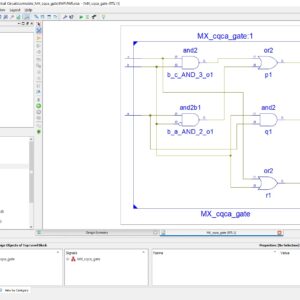
Design of Testable Reversible Sequential Circuits
Abstract: In this paper, we propose the design of two vectors testable sequential circuits based on conservative logic gates. The proposed sequential circuits based on conservative logic gates outperform the sequential circuits implemented in classical gates in terms of testability. Any sequential circuit based on conservative logic gates can be tested for classical unidirectional stuck-at faults using only two test vectors. The two test vectors are all 1s, and all 0s. The designs of two vectors testable latches, master-slave flip-flops and double edge triggered (DET) flip-flops are presented. The importance of the proposed work lies in the fact that it provides the design of reversible sequential circuits completely testable for any stuck-at fault by only two test vectors, thereby eliminating the need for any type of scan-path access to internal memory cells. The reversible design of the DET flip-flop is proposed for the first time in the literature. We also showed the application of the proposed approach toward 100% fault coverage for single missing/additional cell defect in the quantum dot cellular automata (QCA) layout of the Fredkin gate. We are also presenting a new conservative logic gate called multiplexer conservative QCA gate (MX-cqca) that is not reversible in nature but has similar properties as the Fredkin gate of working as 2:1 multiplexer. The proposed MX-cqca gate surpasses the Fredkin gate in terms of complexity (the number of majority voters), speed, and area.
List of the following materials will be included with the Downloaded Backup:
Design of ultra-low power consumption approximate 4-2 compressors based on the compensation characteristic
Abstract:
Approximate computing is tentatively applied in some digital signal processing applications which have an inherent tolerance for erroneous computing results. The approximate arithmetic blocks are utilized in them to improve the electrical performance of these circuits. Multiplier is one of the fundamental units in computer arithmetic blocks. Moreover, the 4-2 compressors are widely employed in the parallel multipliers to accelerate the compression process of partial products. In this paper, three novel approximate 4-2 compressors are proposed and utilized in 8-bit multipliers. Meanwhile, an error-correcting module (ECM) is presented to promote the error performance of approximate multiplier with the proposed 4-2 compressors. In this paper, the number of the approximate 4-2 compressor’s outputs is innovatively reduced to one, which brings further improvements in the energy efficiency. Compared with the exact 4-2 compressors, the simulation results indicate that the proposed approximate compressors UCAC1, UCAC2, UCAC3 achieve 24.76%, 51.43%, and 66.67% reduction in delay, 71.76%, 83.06%, and 93.28% reduction in power and 54.02%, 79.32%, and 93.10% reduction in area, respectively. And the utilization of these proposed compressors in 8-bit multipliers brings 49.29% reduction of power consumption on average.
List of the following materials will be included with the Downloaded Backup: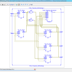
Determining Application-Specific Knowledge for Improving Robustness of Sequential Circuits
Base Paper Abstract:
Due to their shrinking feature sizes as well as environmental influences, such as high-energy radiation, electrical noise, and particle strikes, integrated circuits are getting more vulnerable to transient faults. Accordingly, how to make those circuits more robust has become an essential step in today’s design flows. Methods increasing the robustness of circuits against these faults already exist for a long period of time but either introduce huge additional logic, change the timing behavior of the circuit, or are applicable for dedicated circuits such as microprocessors only. In this paper, we propose an alternative method, which overcomes these drawbacks by determining application specific knowledge of the circuit, namely the relations of flip-flops and when they assume the same value. By this, we exploit partial redundancies, which are inherent in most circuits anyway (even the optimized ones), to frequently compare the circuit signals for their correctness—eventually leading to an increased robustness. Since determining the correspondingly needed information is a computationally hard task, formal methods, such as bounded model checking, satisfiability-based automatic test pattern generation, and binary decision diagrams, are utilized for this purpose. The resulting methodology requires only a slight increase in additional hardware, does only influence the timing behavior of the circuit negligibly, and is automatically applicable to arbitrary circuits. Experimental evaluations confirm these benefits.
List of the following materials will be included with the Downloaded Backup:
DiP: A Scalable, Energy-Efficient Systolic Array for Matrix Multiplication Acceleration
Transformers are gaining increasing attention across Natural Language Processing (NLP) application domains due to their outstanding accuracy. However, these data-intensive models add significant performance demands to the existing computing architectures. Systolic array architectures, adopted by commercial AI computing platforms like Google TPUs, offer energy-efficient data reuse but face throughput and energy penalties due to input-output synchronization via First-In-FirstOut (FIFO) buffers. This paper proposes a novel scalable systolic array architecture featuring Diagonal-Input and Permutated weight stationary (DiP) dataflow for matrix multiplication acceleration. The proposed architecture eliminates the synchronization FIFOs required by state-of-the-art weight stationary systolic arrays. Beyond the area, power, and energy savings achieved by eliminating these FIFOs, DiP architecture maximizes the computational resource utilization, achieving up to 50% throughput improvement over conventional weight stationary architectures. Analytical models are developed for both weight stationary and DiP architectures, including latency, throughput, time to full PEs utilization (TFPU), and FIFOs overhead. A comprehensive hardware design space exploration using 22nm commercial technology demonstrates DiP’s scalability advantages, achieving up to a 2.02× improvement in energy efficiency per area. Furthermore, DiP outperforms TPU-like architectures on transformer workloads from widely-used models, delivering energy improvement up to 1.81× and latency improvement up to 1.49×. At a 64×64 size with 4096 PEs, DiP achieves a peak throughput of 8.192 TOPS with energy efficiency 9.548 TOPS/W.
List of the following materials will be included with the Downloaded Backup: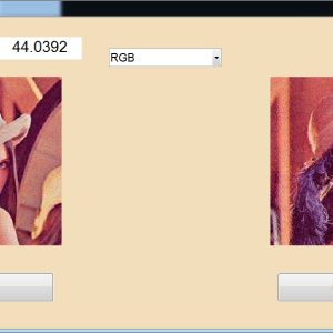
Dual Quality 4:2 Compressor for Utilizing in Dynamic Accuracy Configurable Multipliers
Abstract:
In this paper, we propose four 4:2 compressors, which have the flexibility of switching between the exact and approximate operating modes. In the approximate mode, these dual-quality compressors provide higher speeds and lower power consumptions at the cost of lower accuracy. Each of these compressors has its own level of accuracy in the approximate mode as well as different delays and power dissipations in the approximate and exact modes. Using these compressors in the structures of parallel multipliers provides configurable multipliers whose accuracies (as well as their powers and speeds) may change dynamically during the runtime. The proposed multiplier saves few adder circuits in partial products, and this proposed multiplier is evaluated with an image processing application. In existing thing, to using this multiplier to design image processing evaluation on only luminance based application, but here the proposed work is modified with Gaussian noise reduction with luminance and chrominance based application, this design to implemented in VHDL, and synthesized in Xilinx S6LX9 FPGA and shown the power, area and delay reports.
List of the following materials will be included with the Downloaded Backup:
Dual Use of Power Lines for Design for Testability A CMOS Receiver Design
As the circuit complexity increases, the number of internal nodes increases proportionally, and individual internal nodes are less accessible due to the limited number of available I/O pins. To address the problem, we proposed power line communications (PLCs) at the IC level, specifically the dual use of power pins and power distribution networks for application/ observation of test data as well as delivery of power. A PLC receiver presented in this paper intends to demonstrate the proof of concept, specifically the transmission of data through power lines. The main design objective of the proposed PLC receiver is the robust operation under variations and droops of the supply voltage rather than high data speed. The PLC receiver is designed and fabricated in CMOS 0.18-µm technology under a supply voltage of 1.8V.
List of the following materials will be included with the Downloaded Backup:
Efficient Approximate Floating-Point Multiplier with Runtime Reconfigurable Frequency and Precision
Base Paper Abstract:
Deep Neural Networks (DNNs) perform intensive matrix multiplications but can tolerate inaccurate intermediate results to some degree. This makes them a perfect target for energy reduction by approximate computing. However, current research in this direction requires DNNs redesign and does not provide the flexibility for users to trade accuracy for energy saving. In this brief, we propose a runtime reconfigurable approximate floating-point multiplier and present details of its hardware implementation. The flexible computation precision is provided by our error correction module, which is controlled by reconfigurable clock signals. The circuit design solves the glitch and metastability problems. The proposed approximate multiplier with three precision levels is evaluated on Synopsys design compiler and Xilinx FPGA platforms. Experimental results demonstrate the advantages of our approach in terms of speed, hardware overhead, and power consumption, while ensuring a controllable accuracy loss for DNNs inferences.
List of the following materials will be included with the Downloaded Backup: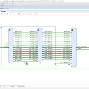
Efficient CRC-BCH Unified Encoder for Global Positioning System
Base Paper Abstract:
GPS uses ECCs to see if an error occurs when the data sent from the satellite reaches the user. Each message structure uses ECCs such as Hamming Code, CRC, BCH Code, and LDPC Code. If the satellite contains all of the encoders, it has a negative impact to the area and power consumption. Therefore, in this paper, we propose a CRC-BCH unified encoder for GPS, which is efficient in terms of space and power consumption. Since both the CRC and BCH encoders use shift registers, the design was made using this part. To replace the existing encoder, the CRC-BCH encoder must have the same output. To validate this, we used individual CRC and BCH encoders and confirmed that the generated output was identical to the output of the proposed encoder. The proposed CRC-BCH unified encoder was synthesized at an operating frequency of 400 MHz using the CMOS 28nm process. The synthesis results showed that it used 16.67% less area and consumed 19.68% less power than the existing encoder. Therefore, the proposed CRC-BCH unified encoder offers advantages in terms of satellite weight and energy efficiency.
List of the following materials will be included with the Downloaded Backup:
Efficient Design for Fixed-Width Adder-Tree
Abstract:
Conventionally, fixed-width adder-tree (AT) design is obtained from the full-width AT design by employing direct or post-truncation. In direct-truncation, one lower order bit of each adder output of full-width AT is post-truncated, and in case of post-truncation, {p} lower order-bits of final-stage adder output are truncated, where p = dlog2 Ne and N is the input-vector size. Both these methods do not provide an efficient design. In this paper, a novel scheme is presented to obtain fixed-width AT design using truncated input. A bias estimation formula based on probabilistic approach is presented to compensate the truncation error. The proposed fixed-width AT design for input-vector sizes 8 and 16 offers (37%, 23%, 22%) and (51%, 30%, 27%) area delay product (ADP) saving for word-length sizes (8, 12, 16), respectively, and calculates the output almost with the same accuracy as the post-truncated fixed-width AT which has the highest accuracy among the existing fixed-width AT. Further, we observed that Walsh-Hadamard transform based on the proposed fixed-width AT design reconstruct higher-texture images with higher peak signal to noise ratio (PSNR) and moderate-texture images with almost the same PSNR compared to those obtained using the existing AT designs. Besides, the proposed design creates an additional advantage to optimize other blocks appear at the upstream of the AT in a complex design.
List of the following materials will be included with the Downloaded Backup:
Efficient Design of Behavioral Clock Divider for Multiple Frequency
Proposed Abstract:
Frequency dividers are of utmost importance in frequency synthesizers that are based on phase locked loops. The use of dual modulus presales enhances the versatility of the design in both integer and Fractional-N frequency synthesizers. The selection of an acceptable division ratio is dependent upon the channel spacing and frequency range of the synthesizer. There are several techniques for division in electronic systems, including the injection locked frequency divider (ILFD), complementary ILFDs, flip flop based dividers, dual modulus dividers, and modular dividers. Therefore, these approaches possess some advantages and disadvantages, such as reduced jitter, a restricted frequency tuning range, increased circuit size due to the addition of an LC tank circuit, increased power consumption, and lower quality factor. This work aims at addressing certain issues pertaining to clock dividers and proposes a unique design that utilizes a multiple digital frequency divider based on D flip flops. The architectural design is predicated on the use of a phase shifting mechanism using a D flip flop, which effectively controls the division ratio. The present study involves the use of a preliminary phase shifting melody in conjunction with the Digital Clock Manager (DCM). The auto tuning strategy described in this study aims to adjust the phase difference between two differential clock signals. By intentionally inducing metastability in one or more flip flops, the proposed approach utilizes a digital clock manager in a clock divider to mitigate the effects of metastability and reduce jitter across multiple tuning frequencies. Furthermore, it is worth noting that the logic size and power consumption required for its operation are significantly reduced.
List of the following materials will be included with the Downloaded Backup: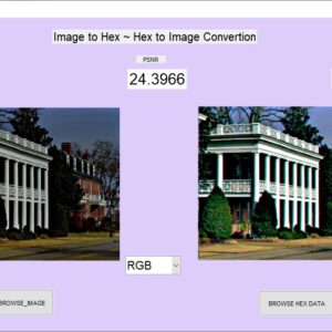
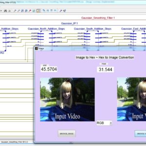
Efficient Image Conversion and Restoration System with Hexadecimal Encoding and Quality Evaluation
Abstract:
The proposed work aims to facilitate the conversion of images into a hexadecimal format for efficient storage and manipulation, and subsequently restore them to their original form. This conversion is beneficial for reducing storage space and simplifying data transmission. The system supports multiple color spaces, including grayscale, RGB, and YCbCr, enhancing its versatility in image processing tasks. Users select an image file, which the system processes according to the selected mode: converting the image or its channels to a hexadecimal format and saving the data to files. During restoration, the system reads the hexadecimal files, reconstructs the image, and displays it. To ensure the fidelity of the restored images, the system computes and displays quality metrics such as Peak Signal-to-Noise Ratio (PSNR), Mean Squared Error (MSE), and Structural Similarity Index (SSIM). This comprehensive solution provides an efficient method for image data handling and quality assessment, ensuring accurate and reliable image restoration.
Proposed System:The proposed system aims to facilitate the conversion of images into a hexadecimal format and subsequently restore them to their original form. This system supports multiple color spaces, including grayscale, RGB, and YCbCr, and evaluates the quality of the restored images using metrics such as Peak Signal-to-Noise Ratio (PSNR), Mean Squared Error (MSE), and Structural Similarity Index (SSIM).
List of the following materials will be included with the Downloaded Backup: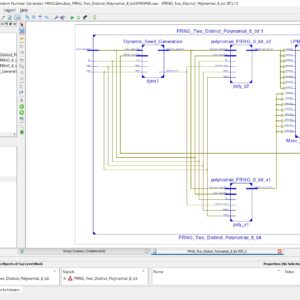
Efficient Pseudo Random Number Generator (PRNG) Design on FPGA
Proposed Abstract:
Random Number Generators (RNGs) are substantially used in many security domains, providing a fundamental source of unpredictability essential for tasks such as cryptography, simulations, and statistical analyses. The efficiency and quality of an RNG directly impact the reliability and security of diverse applications, making advancements in RNG design, as explored in this study, of significant importance for enhancing computational processes. This paper presents an innovative Pseudo-Random Number Generator (PRNG) that leverages the efficiency of two carefully selected Linear Feedback Shift Registers (LFSRs) and a connecting XOR gate. The investigation of five polynomials identified an optimal pair, resulting in a notable improvement of over 200X in the length of random bit sequences compared to a single LFSR-based PRNG. The Basys3 FPGA board with the xc7a35tcpg236-1 FPGA chip was used to implement and synthesize the proposed design. Two significant findings emerge from this research. Firstly, using variable polynomials demonstrates a huge enhancement in the duration of randomness, outperforming the impact of variable seeds. A noteworthy observation is that employing the same polynomials in different branches does not result in optimal results. Secondly, managing more seeds is associated with an increased area cost, underscoring the efficiency of handling two polynomials.
List of the following materials will be included with the Downloaded Backup:
Efficient Super Resolution Algorithm using Overlapping Bi-cubic Interpolation
Abstract:
In practical CCTV applications, there are problems of the camera with low resolution, camera fields of view, and lighting environments. These could degrade the image quality and it is difficult to extract useful information for further processing. Super-resolution techniques have been proposed widely by the researchers. However, many approaches are complex and are difficult to use in practical scenarios. In this paper, we propose an efficient Super-resolution algorithm using overlapping bi-cubic for hardware implementation. Experimental results are verified using processing time and reconstructed images that can be used in real time applications.
List of the following materials will be included with the Downloaded Backup:
Efficient TCAM Design Based on Multipumping Enabled Multiported SRAM on FPGA
Abstract:
Ternary content-addressable memory (TCAM)-based search engines play an important role in networking routers. The search space demands of TCAM applications are constantly rising. However, existing realizations of TCAM on field-programmable gate arrays (FPGAs) suffer from storage inefficiency. This paper presents a multipumping-enabled multiported SRAM-based TCAM design on FPGA, to achieve an efficient utilization of SRAM memory. Existing SRAM-based solutions for TCAM reduce the impact of the increase in the traditional TCAM pattern width from an exponential growth in memory usage to a linear one using cascaded block RAMs (BRAMs) on FPGA. However, BRAMs on state-of-the-art FPGAs have a minimum depth limitation, which limits the storage efficiency for TCAM bits. Our proposed solution avoids this limitation by mapping the traditional TCAM table divisions to shallow sub-blocks of the configured BRAMs, thus achieving a memory-efficient TCAM memory design. The proposed solution operates the configured simple dual-port BRAMs of the design as multiported SRAM using the multipumping technique, by clocking them with a higher internal clock frequency to access the sub-blocks of the BRAM in one system cycle. We implemented our proposed design on a Virtex-6 xc6vlx760 FPGA device. Compared with existing FPGA-based TCAM designs, our proposed method achieves up to 2.85 times better performance per memory.
List of the following materials will be included with the Downloaded Backup:
Energy Efficient Compact Approximate Multiplier for Error-Resilient Applications
Base Paper Abstract:
The primary goal of approximate computing is enhancing system performance, such as energy efficiency, speed, and form factor. Despite the growing use of approximate multipliers, the design of efficient approximate compressors — a fundamental multiplier block — remains a significant challenge. In this brief, 8-transistor and 14-transistor 4:2 compressors are proposed. Both compressors exploit CMOS technology and a constant and conditional approximation of selected inputs, exhibiting fewer negative errors. As a result, a resource-expensive error recovery module is eliminated, yielding superior performance as compared with prior art. The 14-transistor architecture yields a lower error rate compared to the 8-transistor architecture, trading off lower area for higher accuracy. The compressor tailored circuit architecture is also proposed and evaluated using image multiplication. The proposed multiplier exhibits 50% area savings and 93% lower power-delay-product compared to the exact multiplier, as well as higher accuracy, and 38% PDP enhancement compared with the state-of-the-art.
List of the following materials will be included with the Downloaded Backup:
Energy-Efficient Approximate Multiplier Design using Bit Significance-Driven Logic Compression
Abstract:
Approximate arithmetic has recently emerged as a promising paradigm for many imprecision-tolerant applications. It can offer substantial reductions in circuit complexity, delay and energy consumption by relaxing accuracy requirements. In this paper, we propose a novel energy-efficient approximate multiplier design using a significance-driven logic compression (SDLC) approach. Fundamental to this approach is an algorithmic and configurable lossy compression of the partial product rows based on their progressive bit significance. This is followed by the commutative remapping of the resulting product terms to reduce the number of product rows. As such, the complexity of the multiplier in terms of logic cell counts and lengths of critical paths is drastically reduced. A number of multipliers with different bit-widths (4-bit to 128-bit) are designed in System Verilog and synthesized using Synopsys Design Compiler. Post-synthesis experiments showed that up to an order of magnitude energy savings, and reductions of 65% in critical delay and almost 45% in silicon area can be achieved for a 128-bit multiplier compared to an accurate equivalent. These gains are achieved with low accuracy losses estimated at less than 0.00071 mean relative error. Additionally, we demonstrate the energy-accuracy trade-offs for different degrees of compression, achieved through configurable logic clustering. In evaluating the effectiveness of our approach, a case study image processing application showed up to 68.3% energy reduction with negligible losses in image quality expressed as peak signal-to-noise ratio (PSNR).
List of the following materials will be included with the Downloaded Backup: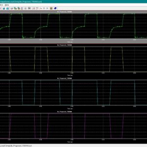
Energy-Efficient Buffer-Based Ternary SRAM Cell With Application to Image Processing
Base Paper Abstract:
This paper presents a design of a variation-resilient and energy-efficient ternary memory cell (TSRAM) suited for power-demanding internet-of-things (IoT) applications that run on batteries. The TSRAM cell utilizes a latch composed of an efficient ternary buffer (TBUF) with positive feedback, a single bit line, and a transmission gate for switching access, with an overall area only about 39% more than binary 6T SRAM. The threshold voltage (Vth) tuning of carbon nanotube field-effect transistor (CNTFET) devices has been explored to achieve the three storage levels. Simulations were conducted using the standard Stanford 32-nm CNTFET model file in the Synopsis HSPICE simulator. The projected design offers substantial reductions of 54.94% in real power, 67.06% in write power, and 21.59% in area compared to the best buffer-based TSRAM designs. These power savings are achieved by minimizing the transistor count and eliminating any direct current path between VDD and ground in the TBUF design for getting logic ‘1’. Furthermore, the proposed design demonstrates the highest logic ‘1’ static noise margin (SNM1) and shows resilience to process, voltage, and temperature (PVT) variations. The TSRAM electrical quality matrix (TEQM), a crucial figure of merit, indicates the superior performance of the proposed design for IoT applications. The study was further extended to conduct simulations and report the performance metrics of the proposed TSRAM array. Ultimately, to evaluate the real-world application of the triple memory structures, the pixel-by-pixel storage process of a grayscale image with three-value data content is performed based on a hardware algorithm. The obtained results demonstrate that the proposed TSRAM architecture has about a 26.3% improvement in hardware performance compared to its highest performing counterpart scheme.
List of the following materials will be included with the Downloaded Backup:
Energy-Efficient VLSI Realization of Binary64 Division With Redundant Number Systems
Base Paper Abstract:
VLSI realizations of digit-recurrence binary division usually use redundant representation of partial remainders and quotient digits. The former allows for fast carry-free computation of the next partial remainder, and the latter leads to less number of the required divisor multiples. In studying the previous relevant works, we have noted that the binary carry save (CS) number system is prevalent in the representation of partial remainders, and redundant high radix representation of quotient digits is popular in order to reduce the cycle count. In this paper, we explore a design space containing four division architectures. These are based on binary CS or radix-16 signed digit (SD) representations of partial remainders. On the other hand, they use full or partial pre computation of divisor multiples. The latter uses smaller multiplexer at the cost two extra adders, where one of the operands is constant within all cycles. The quotient digits are represented by radix-16 [−9,9]SDs. Our synthesis-based evaluation of VLSI realizations of the best previous relevant work and the four proposed designs show reduced power and energy figures in the proposed designs at the cost of more silicon area and delay measures. However, our energy-delay product is 26%–35% less than that of the reference work.
List of the following materials will be included with the Downloaded Backup:
Energy-Quality Scalable Adders Based on Non-zeroing Bit Truncation
Abstract:
Approximate addition is a technique to trade off energy consumption and output quality in error-tolerant applications. In prior art, bit truncation has been explored as a lever to dynamically trade off energy and quality. In this brief, an innovative bit truncation strategy is proposed to achieve more graceful quality degradation compared to state-of-the-art truncation schemes. This translates into energy reduction at a given quality target. When applied to a ripple-carry adder, the proposed bit truncation approach improves quality by up to 8.5 dB in terms of peak signal-to-noise ratio, compared to traditional bit truncation. As a case study, the proposed approach was applied to a discrete cosine transform engine. In comparison with prior art, the proposed approach reduces energy by 20%, at insignificant delay and silicon area overhead.
List of the following materials will be included with the Downloaded Backup:
ER-TCAM: A Soft-Error-Resilient SRAM-Based Ternary Content-Addressable Memory for FPGAs
Abstract:
Static random access memory (SRAM)-based ternary content-addressable memory (TCAM) on field-programmable gate arrays (FPGAs) is used for packet classification in software-defined networking (SDN) and Open Flow applications. SRAMs implementing TCAM contents constitute the major part of a TCAM design on FPGAs, which are vulnerable to soft errors. The protection of SRAM-based TCAMs against soft errors is challenging without compromising critical path delay and maintaining a high search performance. This brief presents a low cost and low-response-time technique for the protection of SRAM-based TCAMs. This technique uses simple, single-bit parity for fault detection which has a minimal critical path overhead. This technique exploits the binary-encoded TCAM table maintained in SRAM-based TCAMs for update purposes to implement a low-response-time error-correction mechanism at low cost. The error-correction process is carried out in the background, allowing lookup operations to be performed simultaneously, thus maintaining a high search performance. The proposed technique provides protection against soft errors with a response time of 293 ns, whereas maintaining a search rate of 222 million searches per second on a 1024 × 40 size TCAM on Artix-7 FPGA.
List of the following materials will be included with the Downloaded Backup: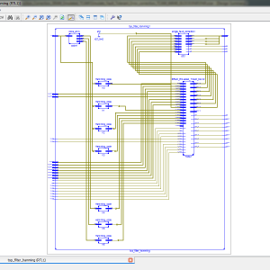
Error Detection and Correction in SRAM Emulated TCAMs
Abstract:
Ternary content addressable memories (TCAMs) are widely used in network devices to implement packet classification. They are used, for example, for packet forwarding, for security, and to implement software-defined networks (SDNs). TCAMs are commonly implemented as standalone devices or as an intellectual property block that is integrated on networking application-specific integrated circuits. On the other hand, field-programmable gate arrays (FPGAs) do not include TCAM blocks. However, the flexibility of FPGAs makes them attractive for SDN implementations, and most FPGA vendors provide development kits for SDN. Those need to support TCAM functionality and, therefore, there is a need to emulate TCAMs using the logic blocks available in the FPGA. In recent years, a number of schemes to emulate TCAMs on FPGAs have been proposed. Some of them take advantage of the large number of memory blocks available inside modern FPGAs to use them to implement TCAMs. A problem when using memories is that they can be affected by soft errors that corrupt the stored bits. The memories can be protected with a parity check to detect errors or with an error correction code to correct them, but this requires additional memory bits per word. In this brief, the protection of the memories used to emulate TCAMs is considered. In particular, it is shown that by exploiting the fact that only a subset of the possible memory contents are valid, most single-bit errors can be corrected when the memories are protected with a parity bit.
List of the following materials will be included with the Downloaded Backup: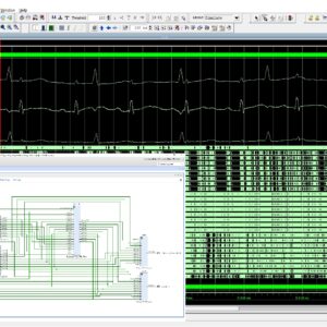
Extraction of Fetal ECG from Abdominal and Thorax ECG Using a Non-Causal Adaptive Filter Architecture
Base Paper Abstract:
Extracting the Electrocardiogram (ECG) of a fetus from the ECG signal of the maternal abdomen is a challenging task due to different artifacts. The paper proposes a N-tap non-causal adaptive filter (NC-AF) that update the weight by considering the N number of past weights and N − 1 number of the reference signal and error signal samples after the processing sample number n. Using the maternal abdominal signal as the primary signal and thorax signal as the reference input, the output e(n) is obtained from the mean of N number of errors. The filtering performance of NC-AF was evaluated using the Synthetic dataset and Daisy dataset with the metrics such as correlation coefficient (γ), peak root mean square difference (PRD), the output signal to noise ratio (SNR), root mean square error (RMSE), and fetal R-peak detection accuracy (FRPDA). The NC-AF provides a maximum correlation coefficient, PRD, SNR, RMSE and FRPDA of 0.9851, 83.04%, 8.52 dB, 0.208 and 97.09% respectively with filter length N = 38. The paper also proposes the architecture of NC-AF that can be implemented in hardware like FPGA. Further, the NC-AF was implemented on Virtex-7 FPGA and its performance is evaluated in terms of resource utilization, throughput, and power consumption. For filter length N = 38 and word length L = 24, the maximum performance of the filter can be attained with a power consumption of 1.287W and a maximum clock frequency of 139.47 MHz.
List of the following materials will be included with the Downloaded Backup: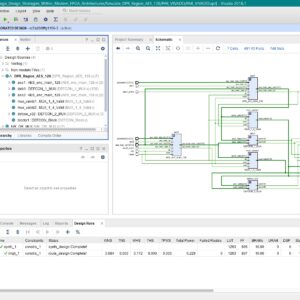
Fail Safe Logic Design Strategies Within Modern FPGA Architectures
Fail-safe computing refers to computing systems that revert to a non-operational safe state when a fault occurs. In this paper, we investigate a circuit level technique as mitigation for single event upsets (SEUs) and fault injection attacks on field programmable gate arrays (FPGAs), and analyze the effectiveness of the technique as a fail-safe monitor for an encryption algorithm. The propagation of fault effects through FPGA primitives including lookup tables (LUTs) and programmable interconnect points (PIPs) is assessed within an FPGA architecture created using an open source tool, and validated using fault injection experiments on an FPGA. The analysis reveals additional vulnerabilities exist within reconfigurable architectures over those in equivalent fail-safe application specific integrated circuit (ASIC), thus requiring a more elaborate network of redundant circuits and checking logic. The configuration memory bits (CMBs), which configure routing and designate logic functions within the LUTs of the FPGA, add complexity to fail-safe design strategies by introducing additional fault conditions and fault propagation paths. A resource efficient fail-safe circuit design technique called Design for Fail-safe in reconfigurable systems (DEFCON) is proposed. The benefits and limitations associated with DEFCON are described in the context of fault injection experiments carried out as simulations and in FPGA hardware.
List of the following materials will be included with the Downloaded Backup: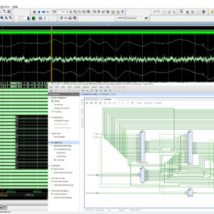
Fast and Hardware-Efficient Variable Step Size Adaptive Beamformer
Base Paper Abstract:
Constant step size least mean square (CSS-LMS) is one of the most popular adaptive beamforming algorithms. However, for varying channel signal-to-noise ratios (SNRs), the CSS algorithms are not effective, and there is a need for variable step size (VSS) algorithms. The VSS algorithms provide extremely deep nulls for the interferences; however, they are complex to implement on hardware. Hence, this paper proposes two hardware-efficient variable step size algorithms, namely, efficient variable step size LMS (EVSS-LMS) and reduced complexity parallel LMS (EVSS-RC-pLMS). The proposed EVSS algorithms eliminate the complex operations of VSS algorithms like division and exponential and approximate them to simpler operations. Further, MATLAB simulations demonstrate accelerated convergence, deep nulls, a lower error floor, and better performance in varying SNR environments for the proposed algorithms. Additionally, the finite precision radiation patterns are similar to infinite precision. Hardware synthesis results show the outstanding performance of EVSS in terms of resource utilization on the Xilinx Artix-7 FPGA.
List of the following materials will be included with the Downloaded Backup: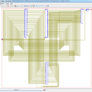
Feed forward-Cutset-Free Pipelined Multiply–Accumulate Unit for the Machine Learning Accelerator
Abstract:
Multiply–accumulate (MAC) computations account for a large part of machine learning accelerator operations. The pipelined structure is usually adopted to improve the performance by reducing the length of critical paths. An increase in the number of flip-flops due to pipelining, however, generally results in significant area and power increase. A large number of flip-flops are often required to meet the feed forward-cutset rule. Based on the observation that this rule can be relaxed in machine learning applications, we propose a pipelining method that eliminates some of the flip-flops selectively. The simulation results show that the proposed MAC unit achieved a 20% energy saving and a 20% area reduction compared with the conventional pipelined MAC.
List of the following materials will be included with the Downloaded Backup: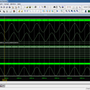
FIR Filter Design based on FPGA
Abstract:
FIR (Finite Impulse Response) Filters: the finite impulse response filter is the most basic components in digital signal processing systems are widely used in communications, image processing, and pattern recognition. Based on FPGA(editable logic device) to achieve FIR filter, not only take into account the fixed -function DSP-specific chip real-time, but also has the DSP processor flexibility. The combination of FPGA and DSP technology can further improve integration, increase work speed and expand system capabilities.
List of the following materials will be included with the Downloaded Backup: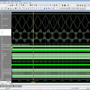
Floating Point Butterfly Architecture Based on Binary Signed Digit Representation
Fast Fourier transform (FFT) coprocessor, having a significant impact on the performance of communication systems, has been a hot topic of research for many years. The FFT function consists of consecutive multiply add operations over complex numbers, dubbed as butterfly units. Applying floating-point (FP) arithmetic to FFT architectures, specifically butterfly units, has become more popular recently. It offloads compute-intensive tasks from general-purpose processors by dismissing FP concerns (e.g., scaling and overflow/underflow). However, the major downside of FP butterfly is its slowness in comparison with its fixed-point counterpart. This reveals the incentive to develop a high-speed FP butterfly architecture to mitigate FP slowness. This brief proposes a fast FP butterfly unit using a devised FP fused-dot product-add (FDPA) unit, to compute AB±CD±E, based on binary signed-digit (BSD) representation. The FP three-operand BSD adder and the FP BSD constant multiplier are the constituents of the proposed FDPA unit. A carry-limited BSD adder is proposed and used in the three-operand adder and the parallel BSD multiplier so as to improve the speed of the FDPA unit. Moreover, modified Booth encoding is used to accelerate the BSD multiplier. The synthesis results show that the proposed FP butterfly architecture is much faster than previous counterparts but at the cost of more area. The proposed architecture of this paper analysis the logic size, area and power consumption using Xilinx 14.2.
List of the following materials will be included with the Downloaded Backup:
Floating-point discrete wavelet transform-based image compression on FPGA
Abstract:
In the era of data transmission through internet, image compression is considered an active research topic, decreasing the amount of data storage for faster data transfer. In this paper, the hardware implementation of an image compression system using Discrete Wavelet Transform (DWT) is presented. The transposed form Finite Impulse Response (FIR) filter is employed for performing the convolution process, on which the DWT is based. The design is generic to fit for different wavelet types and symmetric to expand for filters of multiple taps. The architecture is implemented on FPGA using IEEE-754 single precision. Floating-Point representation offered higher precision and better accuracy compared to scaled integer values. The proposed hardware design is implemented on Virtex 5 FPGA achieving 243.6 MHz clock frequency.
List of the following materials will be included with the Downloaded Backup: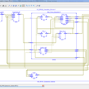
FPGA Based High Definition SPWM Generation With Harmonic Mitigation Property
Abstract:
High-resolution sinusoidal pulse width modulation (SPWM) switching is beneficial in order to achieve compact size and fine sinusoidal output of dc–ac converters. In this article, a novel field-programmable gate array (FPGA) based high-definition SPWM (HD-SPWM) architecture is proposed for adopting a scheme of integrating a lower frequency PWM train to a high-frequency SPWM train in order to suppress inverter output harmonics while achieving high resolution output. An optimized FPGA based two-stage finite-state-machine (FSM) architecture is designed, where the initial stage decides pulse widths of a lower frequency PWM train based on the premeditated pulse width of the high-frequency SPWM train, whereas in the final stage, lower frequency PWM pulse widths are integrated with the high-frequency SPWM pulse widths to generate updated pulse widths of high-frequency SPWM, i.e., HD-SPWM. Moreover, a pre-formulation mathematical model is established for the calculation of duty-cycle count values of pulse trains to support the online adjustment of modulation index (MI) of the HD-SPWM. The proposed generation has the benefits of harmonic mitigation, online fine adjustment of MI, low-processing time, and requirement of a minor segment of a medium-sized FPGA; thereby, providing a good tradeoff between larger designs and higher performance. Theoretical calculations, characteristics, and design contemplations are specified, and the HD-SPWM generation is demonstrated through experimentation with a Xilinx Spartan-3 FPGA board.
List of the following materials will be included with the Downloaded Backup: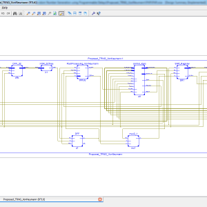
FPGA Based True Random Number Generation Using Programmable Delays in Oscillator Rings
Abstract:
True random number generators play a fundamental role in cryptographic systems. This paper presents a new and efficient method to generate true random numbers on field programmable gate array by utilizing the random jitter of free running oscillators as a source of randomness. The free-running oscillator rings incorporate programmable delay lines to generate large variation of the oscillations and to introduce jitter in the generated ring oscillators clocks. The main advantage of the proposed true random number generator utilizing programmable delay lines is to reduce correlation between several equal length oscillator rings, and thus improve the randomness qualities. In addition, a Von Neumann corrector as post-processor is employed to remove any bias in the output bit sequence. The validation of the proposed approach is demonstrated on Xilinx Spartan-3A FPGAs. The proposed true random number generator occupies 528 slices, achieves 6 Mbps throughput with 0.999 per bit entropy rate, and passes all the National Institute of Standards and Technology (NIST) statistical tests.
List of the following materials will be included with the Downloaded Backup: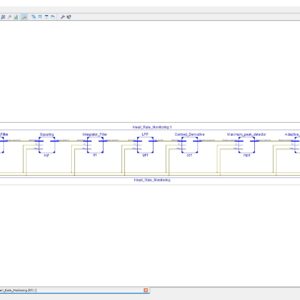
FPGA Heart Rate Monitoring (Pre Processing – QRS Detection Stage)
Base Paper Abstract:
The continuous monitoring of cardiac patients requires an ambulatory system that can automatically detect heart diseases. This study presents a new field programmable gate array (FPGA)-based hardware implementation of the QRS complex detection. The proposed detection system is mainly based on the Pan and Tompkins algorithm, but applying a new, simple, and efficient technique in the detection stage. The new method is based on the centered derivative and the intermediate value theorem, to locate the QRS peaks. The proposed architecture has been implemented on FPGA using the Xilinx System Generator for digital signal processor and the Nexys-4 FPGA evaluation kit. To evaluate the effectiveness of the proposed system, a comparative study has been performed between the resulting performances and those obtained with existing QRS detection systems, in terms of reliability, execution time, and FPGA resources estimation. The proposed architecture has been validated using the 48 half-hours of records obtained from the Massachusetts Institute of Technology - Beth Israel Hospital (MITBIH) arrhythmia database. It has also been validated in real time via the analogue discovery device.
List of the following materials will be included with the Downloaded Backup: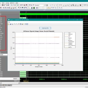
FPGA Implementation for Odor Identification with Depthwise Separable Convolutional Neural Network
Base Paper Abstract:
The integrated electronic nose (e-nose) design, which integrates sensor arrays and recognition algorithms, has been widely used in different fields. However, the current integrated e-nose system usually suffers from the problem of low accuracy with simple algorithm structure and slow speed with complex algorithm structure. In this article, we propose a method for implementing a deep neural network for odor identification in a small-scale Field-Programmable Gate Array (FPGA). First, a lightweight odor identification with depthwise separable convolutional neural network (OIDSCNN) is proposed to reduce parameters and accelerate hardware implementation performance. Next, the OI-DSCNN is implemented in a Zynq-7020 SoC chip based on the quantization method, namely, the saturation-flooring KL divergence scheme (SF-KL). The OI-DSCNN was conducted on the Chinese herbal medicine dataset, and simulation experiments and hardware implementation validate its effectiveness. These findings shed light on quick and accurate odor identification in the FPGA.
List of the following materials will be included with the Downloaded Backup:
FPGA Implementation of 64 Block Data Encryption Standard Algorithm
Proposed Abstract:
The Data Encryption Standard (DES) is widely recognized as the inaugural and prevailing symmetric key method used for the cryptographic processes of encrypting and decrypting digital data. Despite its lack of security against determined attackers in contemporary times, the use of this method persists in older systems. This work introduces a novel implementation of the Data Encryption and Decryption Standard algorithm using Field Programming Gate Arrays (FPGAs) that prioritizes security, high throughput, and space efficiency. The suggested solution involves the creation of a system that utilizes a block size of 64 bits and a key length that is also 64 bits. Additionally, the system operates with a data width of 64 bits. This achievement is accomplished by integrating the notion of pipelining with time variable permutations, and then comparing it with previously shown encryption techniques. The permutations undergo temporal variations under the control of the cryptographer. Hence, the cipher text also undergoes alteration while the key and plaintext remain constant. The algorithm under consideration has been successfully executed on the Xilinx Vetex-5 Field-Programmable Gate Array (FPGA) platform. The findings of this study indicate that the suggested implementation exhibits exceptional speed in comparison to other hardware implementations. Additionally, it demonstrates superior area efficiency and significantly enhanced security measures.
List of the following materials will be included with the Downloaded Backup:
FPGA Implementation of 8×8 Truncated Multiplier
Proposed Abstract:
The operation of multiplication is an often encountered need in the field of digital signal processing. Parallel multipliers provide a rapid approach for performing multiplication operations, while demanding a significant amount of space in VLSI (Very Large Scale Integration) implementations. In the majority of signal processing applications, there is a preference for using a rounded result in order to prevent an increase in the size of the word. Therefore, an important goal in the design process is to minimize the spatial demand of the rounded output multiplier. This study introduces a novel approach to parallel multiplication that efficiently calculates the products of two n-bit values by selectively summing the most important columns using a variable correction technique. This research furthermore includes a comparative analysis of the implementation of 8X8 conventional and truncated multipliers using Verilog Hardware Description Language (HDL) on Field Programmable Gate Arrays (FPGAs). The shortened multiplier demonstrates a much greater decrease in device consumption as compared to the regular multiplier. A conventional multiplier performs computations on n x n bits and produces a weighted sum of the output, consisting of 2n bits. In contrast, a truncated multiplier generates an output of just n bits from the n x n bit input. The use of logic gates in both internal and external hardware design will be decreased. Truncated multipliers provide a viable approach for achieving significant reductions in FPGA resources, latency, and power consumption compared to regular parallel multipliers, particularly in scenarios where the complete accuracy provided by the standard multiplier is unnecessary.
List of the following materials will be included with the Downloaded Backup:
FPGA Implementation of 8×8 Truncated Multiplier Using Brent Kung Parallel Prefix Adder
Proposed Abstract:
Multiplication is a critical operation in many digital signal processing and machine learning applications, where fast and efficient computation is essential. However, conventional multipliers that compute n x n bit products result in significant hardware overhead and increased power consumption. To address these challenges, this paper proposes an FPGA implementation of an 8x8 truncated multiplier utilizing the Brent-Kung parallel prefix adder to improve both speed and resource efficiency. The proposed truncated multiplier limits the output to n bits, discarding the least significant bits and utilizing a variable correction technique to minimize the error introduced by truncation. By selectively summing the most significant columns, the design achieves a balance between accuracy and hardware efficiency, providing a reduced-area solution for approximate computing. The Brent-Kung parallel prefix adder is integrated into the multiplier architecture to optimize the carry propagation stage, reducing the overall critical path delay. This adder is known for its logarithmic depth, which significantly improves the speed of the summation process while using fewer logic gates compared to traditional adders. This design was implemented in Verilog HDL and synthesized on a Xilinx Virtex-5 FPGA platform. Comparative analysis with a conventional multiplier shows that the proposed truncated multiplier achieves a notable reduction in FPGA resource utilization, including logic elements and power consumption, without sacrificing significant accuracy. The architecture particularly suitable for applications where speed and low power consumption are paramount, such as real-time image processing, DSP systems, and machine learning accelerators.
List of the following materials will be included with the Downloaded Backup:
FPGA Implementation of a ECG-DAC-SPI Interface for Medical Applications
Proposed Abstract:
This project presents the design and implementation of an ECG-DAC-SPI interface for medical applications using the Xilinx Spartan-6 FPGA platform and the MCP4921 12-bit SPI DAC. The objective is to process pre-recorded ECG signals from the MIT-BIH database, reconstruct the signal digitally, and output it as an accurate analog waveform suitable for real-time monitoring and simulation. The system is designed to meet the stringent requirements of medical-grade signal fidelity and low-latency processing. The FPGA-based implementation comprises several key modules, including digital ECG data acquisition, optional noise filtering, and a custom SPI communication controller. The ECG signal, preloaded into FPGA memory, is scaled and quantized to match the 12-bit resolution of the MCP4921 DAC. A low-pass FIR filter is implemented on the FPGA to enhance signal quality by removing high-frequency noise, ensuring smooth signal. A Verilog HDL-based SPI controller facilitates precise communication with the DAC, synchronizing data transfer and ensuring real-time signal conversion. The reconstructed analog ECG waveform is visualized on an oscilloscope to validate its fidelity to the original dataset. The DAC, interfaced via the FPGA’s SPI controller, is chosen for its high resolution and compatibility with low-latency applications. The design is synthesized, implemented, and tested on the Xilinx Spartan-6 FPGA platform. The project includes extensive simulation and hardware testing, evaluating parameters such as SPI throughput, waveform accuracy, and system latency. Results demonstrate that the system achieves precise signal reconstruction and reliable analog output, suitable for medical applications. This work highlights the use of FPGA technology and the MCP4921 DAC for scalable and reconfigurable ECG signal processing systems. It provides a robust platform for integration into advanced medical devices, including real-time ECG monitors, simulators, and portable diagnostic tools. Future extensions of the design could include integration of live ECG sensors, advanced noise filtering, or wireless transmission for telemedicine applications.
List of the following materials will be included with the Downloaded Backup:
FPGA Implementation of Comparative Analysis and Performance Evaluation for Different LFSR Techniques
Proposed Abstract:
In this study, we explore the implementation and performance evaluation of various Linear Feedback Shift Register (LFSR) techniques on Field Programmable Gate Arrays (FPGAs). LFSRs are fundamental components in numerous digital applications, including cryptography, pseudorandom number generation, error detection, and secure communications. We specifically focus on five different LFSR methodologies: Fibonacci LFSR, Galois LFSR, Non-Linear Feedback Shift Register (NLFSR), Modular LFSR and Masked LFSR. Each technique is implemented on an FPGA platform, utilizing Verilog HDL for design specification and synthesis. The study begins with a detailed examination of the theoretical underpinnings and operational mechanisms of each LFSR technique, followed by their FPGA implementations. We then conduct a comprehensive performance analysis, focusing on critical parameters such as area utilization, power consumption, throughput, and randomness quality. The analysis reveals the strengths and trade-offs associated with each method, providing insights into their suitability for various applications. Our results demonstrate that while Fibonacci and Galois LFSRs offer simplicity and ease of implementation, more advanced techniques like NLFSR and Masked LFSR provide enhanced security features at the cost of increased complexity. The study concludes with recommendations on selecting the appropriate LFSR technique based on the specific requirements of the application, highlighting the balance between security, performance, and resource efficiency in FPGA-based designs.
List of the following materials will be included with the Downloaded Backup: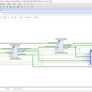
FPGA Implementation of D8PSK Demodulator
Base Paper Abstract:
Differential phase shift keying (DPSK) is a modulation scheme that facilitates non coherent demodulation and is employed for various applications such as Wireless Local Area Networks (WLANs), Bluetooth and RFID communication. In this paper, design, development and hardware implementation of a new demapping scheme for Differential 8-PSK (D8PSK) demodulator on a Zynq 7000 FPGA based ZED board is proposed using the concepts of model based design. The proposed work can be easily extended to other M-ary DPSK schemes.
List of the following materials will be included with the Downloaded Backup: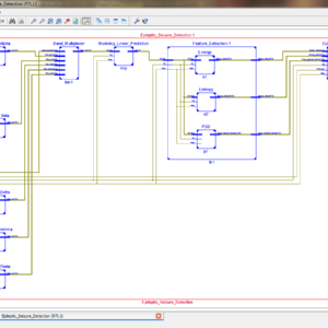
FPGA Implementation of Epileptic Seizure Detection Using ELM Classifier Detection Using ELM Classifier
Abstract:
Electroencephalography (EEG) Signals are widely used to determine the brain disorders. The Electrical activity of human brain is recorded in the form of EEG signal. The abnormal Electrical activity of the human brain is called as epileptic seizure. In epilepsy patients, the seizure occurs at unpredictable times and it causes sudden death. Detection and Prediction of Epileptic seizure is performed by analyzing the EEG signal. The EEG signal of human brain is random in nature, hence detection of seizure in EEG signal is challenging task. Hardware implementation of Epileptic seizure detection system is necessary for real time applications. In this work an accurate approach is used to identify the Epileptic seizure and that is implemented in FPGA (Field Programmable Gate Array).The hardware implementation of epileptic seizure detection algorithm is done using Xilinx System generator tool. In the first step the EEG signal is extracted from the human brain and it is filtered by using Finite Impulse response (FIR) band pass filter. The band pass filter separates the EEG signal into delta, theta, alpha, beta and gamma brain rhythms. The band separated brain signal is modeled by linear prediction theory. In the next step features are extracted from the modeled EEG signal and the classification of normal or seizure signal is done by using Extreme Learning Machine (ELM) classifier. The EEG signals used in this paper were obtained from Epilepsy Center at the University of Bonn, Germany. The hardware architecture, Look up tables, resource utilization, Accuracy and power consumption of the algorithm is analyzed using xilinx zynq7000 all programmable soc.
List of the following materials will be included with the Downloaded Backup:
FPGA Implementation of High Performance Reversible logic based 16×16 Array Multiplier
Proposed Abstract:
In this recent technology of digital gadgets and digital signal processing and image processing method will have more priority in arithmetic operation, such as multiplication, divisions, addition and subtractions. In this operations of arithmetic unit will have number of garbage signal with more memory logic element, due to this problem these arithmetic operations will take more area, delay and power in VLSI system design. Here, this proposed work will present a arithmetic operation using reversible logic method, thus it take memory less logic and less garbage elements, therefore here this reversible logic method will integrated using reversible half adders and full adder in array multiplier and proved the performance with less garbage signals. Finally, this work will have integrated in Verilog HDL, simulated in Modelsim and Synthesized in Xilinx FPGA, and also compared all the parameter in terms of area, delay and power.
List of the following materials will be included with the Downloaded Backup: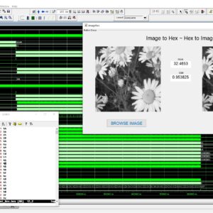
FPGA Implementation of Image Line Buffer to Split and reconstruct a 3×3 size of image pixel with using FIFO Design
Proposed Abstract:
Image line buffers are used in several kinds of image processing applications, particularly where operations must be executed on a per-line basis in order to optimize efficiency. There are many typical applications associated with this technology, including real-time video processing, image filtering, edge detection, computer vision, memory optimization, parallel processing, compression algorithms, and medical imaging. In the context of image and video processing applications, the use of image line buffers may contribute to the optimization of operations when dealing with a continuous stream of frames processed in real time. In the context of image processing, convolutional processes are often used for tasks like as image filtering and blurring. These operations are typically carried out on a per-pixel basis, wherein the value assigned to each pixel is determined by the values of its adjacent pixels. The proposed structure was created using a First-In-First-Out (FIFO) based approach, aiming to decrease the number of logic sizes and complexity in Very Large Scale Integration (VLSI) design architecture. The conversion of design images to hexadecimal and hexadecimal to image format is accomplished using MATLAB GUI applications. These applications also facilitate the comparison of Peak Signal-to-Noise Ratio (PSNR) and Structural Similarity Index Measure (SSIM) values. The internal architecture of the system is implemented using Verilog Hardware Description Language (HDL). Additionally, the simulation is conducted using Modelsim. Furthermore, the system's performance parameters, including area, delay, and power consumption, are compared with those of the Xilinx Vertex-5 Field Programmable Gate Array (FPGA).
List of the following materials will be included with the Downloaded Backup: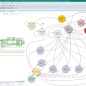
FPGA Implementation of Intelligent Elevator System for AI Applications
Proposed Abstract:
Intelligent elevator systems are used in many smart buildings, offices, hospitals, and tall apartments to move people quickly, reduce waiting time, and save energy. They have many advantages, like faster operation, better safety, and the ability to handle requests from many floors at the same time. But there are also some disadvantages, such as slow response when many people use them, fixed movement patterns that cannot adjust to real-time needs, weak security for restricted floors, and no use of advanced AI features for learning and prediction. Most existing elevator systems are built using microcontrollers with fixed scheduling methods, which cannot easily change their operation or add smart features. The problem in this work is to create an elevator system that works faster, is more secure, can adjust to different situations, and is ready for AI use, while also keeping passengers safe. In this project, we design an elevator controller on FPGA using a finite state machine. The system includes floor request handling, priority scheduling, emergency stop, overload detection, automatic door timing, floor number display, passcode access for special floors, and a fire alarm mode. The new idea in this work is to use the speed and flexibility of FPGA hardware along with an FSM design that can later connect to AI for learning passenger habits and predicting movement needs. This makes the system quick, safe, and adaptable. The design is written in Verilog HDL, tested in ModelSim, and implemented on a Xilinx FPGA board. We measure performance by checking response time, scheduling efficiency, and safety accuracy, and the results show it is suitable for future smart building use.
List of the following materials will be included with the Downloaded Backup:
FPGA implementation of low power and high speed image edge detection algorithm
Abstract:
Image processing is a vital task in data processing system for applications in medical fields, remote sensing, microscopic imaging etc., Algorithms for processing image exist except for real time system style, hardware implementation is most popular principally. This paper presents a design for Sobel filter based edge detection on Field Programmable Gate Array (FPGA) board. Hardware implementation of the Sobel edge detection algorithm is chosen because it presents an honest scope for similarity over software package. On the opposite hand, Sobel edge detection will work with less deterioration in high level of noise. Edges are primarily the noticeable variation of intensities in a picture. Edges facilitate to spot the placement of an object and also the boundary of a selected entity within the image. It conjointly helps in feature extraction and pattern recognition. Hence, edge detection is of nice importance in pc vision. The planned design for edge detection exploitation Sobel algorithm is designed using structural Verilog lipoprotein synthesized exploitation Cadence Genus and enforced using Cadence Innovus. The practicality of the planning is verified exploitation normal pictures by FPGA implementation. The proposed architecture reduce the power, delay and space complexity compare to three existing architectures.
List of the following materials will be included with the Downloaded Backup:
FPGA Implementation of Partially Parallel Encoder Architecture for Long Polar Code
Polar coding is an encoding/decoding scheme that provably achieves the capacity of the class of symmetric binary memory-less channels. Due to the channel achieving property, the polar code has become one of the most favourable error-correcting codes. As the polar code achieves the property asymptotically, however, it should be long enough to have a good error-correcting performance. Although previous fully parallel encoder is intuitive and easy to implement, it is not suitable for long polar codes because of the huge hardware complexity required. In the brief, we analyse the encoding process in the viewpoint of very large-scale integration implementation and propose a new efficient encoder architecture that is adequate for long polar codes and effect in alleviating the hardware complexity. As the proposed encoder allows high-throughput encoding with small hardware complexity, it can be systematically applied to the design of any polar code and to any level of parallelism. Finally shown the power, area, delay report with comparison of existing work.
List of the following materials will be included with the Downloaded Backup:
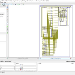
FPGA Implementation of Single Precision Floating Point Multiplier using High Speed Parallel Prefix Adder based Wallace Tree Multiplier
Base Paper Abstract:
In this paper present, an efficient implementation of single precision method of floating point multiplier target for Xilinx Vertex 5 FPGA using Verilog HDL. The floating point implementation will cover up with 23-bit exponent, 8-bit mantissa, and 1 sign bit. This proposed architecture implement with high speed parallel prefix adder based Wallace Tree Multiplier. a Wallace tree multiplication will provide effective terms of low logic sizes and more speed of operations. In a recent arithmetic applications based circuit design will have more demand with high speed and low area, in this manner the proposed approach of this work will improve the speed of Wallace tree multiplier using 4:2 compressor method without degrading its area parameter. Thus, the proposed method will integrate more efficient and more reliable Kogge stone parallel prefix, Brent kung parallel prefix, Sklansky parallel prefix addition operation in the Wallace tree multiplication on final addition stage at 16-bit data width. Finally, done this floating point multiplier architecture with Wallace tree architecture included normalized rounding method and to reduce area, delay and power. The error difference will have analyzed using Modelsim Software, and analyses optimized logic size's, delay and power consumptions.
List of the following materials will be included with the Downloaded Backup: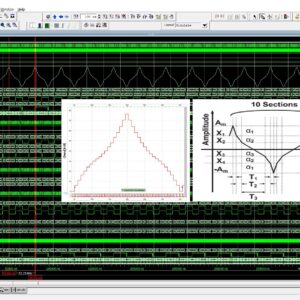
FPGA Implementation of Spread Spectrum Clock Generator with Onion Modulation
Proposed Abstract:
A Spread Spectrum Clock Generator (SSCG) is used in electronics to purposefully vary the frequency of a clock signal via modulation. Modulation is accomplished by dispersing the energy of the signal throughout a spectrum of frequencies rather than focusing it on a certain frequency. The main objective of using the spread spectrum approach in clock generation is to minimize electromagnetic interference (EMI) and enhance electromagnetic compatibility (EMC) in electronic systems. The main reason for using many layers of modulation in spread spectrum clock production, regardless of whether the name "Onion Modulation" is used, is to provide a more advanced and adaptable method for reducing electromagnetic interference. The primary design feature of the onion wave is that the core portion of the waveform has the least steep slope, which serves to generate the output. In order to optimize the frequency effect design, the conventional approach involves using a memory ROM to regulate the slope and obtain the desired onion waveform. This current methodology necessitates substantial memory allocation and an intricate architecture, resulting in higher power consumption. The proposed method presents a unique architecture for onion modulation, which offers reduced logic size and power usage. This architecture was created using Verilog HDL, tested using Modelsim, and implemented using the Xilinx Vertex-5 FPGA.
List of the following materials will be included with the Downloaded Backup: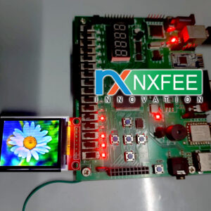
FPGA Implementation of TFT 1.8 inch SPI 128×160 Display ROM Interface
Simple Description:
This ST7735R is a display controller used in small TFT (Thin-Film Transistor) LCD displays. It is often used in combination with microcontrollers or FPGAs to drive these displays. The controller supports the Serial Peripheral Interface mode of communication for sending commands and data to the display. This TFT display helps with a greater number of image and video processing applications. Here we have implemented this TFT display in FPGA hardware implementation using Verilog HDL with a novelty-based architecture design. Finally shown the output with TFT Display.
List of the following materials will be included with the Downloaded Backup:
FPGA Implementation of the Adaptive Digital Beamforming for Massive Array
Base Paper Abstract:
With the rise of 5G networks and the increasing number of communication devices, improving communication quality is essential. One approach is adaptive digital beamforming, which adjusts an antenna array’s radiation pattern based on the desired received signal. Adaptation based on Least-Mean Squared (LMS) and its variants is still one of the most common literature methods. Although LMS techniques present good computational performance, the increase in antennas’ numbers led to high-performance hardware. Platforms such as Field Programmable Gate Arrays (FPGAs), designed for massive array systems, enables high-performance energy-efficient architectures. This work proposes a parallel implementation of a massive array beamforming composed of a spatial filter and adaptation unit based on LMS on FPGA. The proposed design presents ten times fewer hardware requirements and 30 times less power consumption than state of the art.
List of the following materials will be included with the Downloaded Backup:
FPGA IP Core for DC Motor Control with Adaptive Neural Network PID Tuning
Base paper Abstract:
Traditional proportional integral derivative (PID) falls short for precise control of DC motor speed under changing conditions. This paper presents a novel FPGA based IP (intellectual property) core for real-time PID parameter adjustment utilizing a multilayer neural network and the back propagation neural network algorithm. The design is implemented entirely in verilog HDL (hardware description language) using the Vivado 2023.1 tool in the Zynq 7z020 SoC (system on chip), with highly efficient resource utilization of 7.37% look-up table (LUT), 1.92% flip-flops, and 3.57% memory. The co-simulation results show a fast rise time of 0.00496s, a settling time of 0.0083s, a lower integral absolute error (IAE) of 0.045, and a minimum overshoot of 0.45%, validating the effectiveness of the proposed controller for comprehensive motion control systems. This dynamic approach outperforms traditional PID controllers by adapting to changing conditions, significantly improving rise time and settling time, which are critical factors in healthcare applications. Other key features of this work include precise duty cycle generation at a 10 kHz switching frequency for accurate motor speed control and an incremental encoder interface for high-resolution position feedback.
List of the following materials will be included with the Downloaded Backup: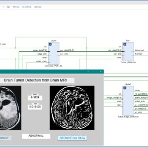
FPGA-Based Brain Tumor Detection from MRI Using 3×3 Convolution Soft IP Core with Stride 1
Base Paper Abstract:
This paper presents an efficient FPGA-based system for automatic brain tumor detection from MRI images using a 3x3 convolutional edge detection method with stride 1. The proposed architecture is developed as a soft IP core in Verilog HDL and synthesized on a Xilinx Zynq 7000 FPGA platform. The system applies a customized 3x3 convolution kernel over each MRI image with stride 1, ensuring that every pixel is processed and fine image details are preserved for accurate tumor detection. Edge detection results are used to segment and highlight abnormal regions, and a thresholding mechanism is employed to differentiate between normal and abnormal images. Hardware resource utilization—including look-up tables (LUTs), flip-flops (FFs), and power consumption—is analyzed after synthesis to verify system efficiency. Experimental results confirm that the proposed FPGA implementation provides real-time processing and reliable brain tumor detection with low power usage, making it suitable for portable and embedded medical devices. The stride 1 approach guarantees maximum detection accuracy and detailed edge representation in all test cases.
List of the following materials will be included with the Downloaded Backup:
FPGA-Based System For Heart Rate Monitoring
Abstract:
The continuous monitoring of cardiac patients requires an ambulatory system that can automatically detect heart diseases. This study presents a new field programmable gate array (FPGA)-based hardware implementation of the QRS complex detection. The proposed detection system is mainly based on the Pan and Tompkins algorithm, but applying a new, simple, and efficient technique in the detection stage. The new method is based on the centred derivative and the intermediate value theorem, to locate the QRS peaks. The proposed architecture has been implemented on FPGA using the Xilinx System Generator for digital signal processor and the Nexys-4 FPGA evaluation kit. To evaluate the effectiveness of the proposed system, a comparative study has been performed between the resulting performances and those obtained with existing QRS detection systems, in terms of reliability, execution time, and FPGA resources estimation. The proposed architecture has been validated using the 48 half-hours of records obtained from the Massachusetts Institute of Technology - Beth Israel Hospital (MITBIH) arrhythmia database. It has also been validated in real time via the analogue discovery device.
List of the following materials will be included with the Downloaded Backup: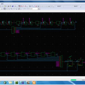
Frequency-Boost Jitter Reduction for Voltage-Controlled Ring Oscillators
Ring oscillators (ROs) are popular due to their small area, modest power, wide tuning range, and ease of scaling with process technology. However, their use in many applications is limited due to poor phase noise and jitter performance. Thermal noise and flicker noise contribute jitter that decreases inversely with oscillation frequency. This paper describes a frequency boost technique to reduce jitter in ROs. We boost the internal oscillation frequency and introduce a frequency divider following the oscillator to maintain the desired output frequency. This approach offers reduced jitter as well as the opportunity to trade off output jitter with power for dynamic performance management. The oscillator has 32 operating modes, corresponding to different values for the ring size and frequency division. In a 0.5-µm CMOS process, the highest oscillation frequency achieved is 25 MHz with a root-mean-square period jitter of 54 ps and a power consumption of 817 µW at 5 V supply. A jitter model for current-starved oscillators was derived and verified by measurement; a direct relationship between oscillation frequency and jitter was derived and measured. Compared with other oscillators, this design achieves the highest performance in terms of jitter per unit interval and figure-of-merit. The performance is expected to improve in more advanced technologies. The results are summarized to offer design guidance based on the frequency boost technique. The proposed architecture of this paper area and power consumption analysis using tanner tool.
List of the following materials will be included with the Downloaded Backup:
Full Swing Local Bitline SRAM Architecture Based on the 22 nm FinFET Technology for Low Voltage Operation
The previously proposed average-8T static random access memory (SRAM) has a competitive area and does not require a write-back scheme. In the case of an average-8T SRAM architecture, a full-swing local bitline (BL) that is connected to the gate of the read buffer can be achieved with a boosted wordline (WL) voltage. However, in the case of an average-8T SRAM based on an advanced technology, such as a 22-nm FinFET technology, where the variation in threshold voltage is large, the boosted WL voltage cannot be used, because it degrades the read stability of the SRAM. Thus, a full-swing local BL cannot be achieved, and the gate of the read buffer cannot be driven by the full supply voltage (VDD), resulting in a considerably large read delay. To overcome the above disadvantage, in this paper, a differential SRAM architecture with a full-swing local BL is proposed. In the proposed SRAM architecture, full swing of the local BL is ensured by the use of cross-coupled pMOSs, and the gate of the read buffer is driven by a full VDD, without the need for the boosted WL voltage. Various configurations of the proposed SRAM architecture, which stores multiple bits, are analyzed in terms of the minimum operating voltage and area per bit. The proposed SRAM that stores four bits in one block can achieve a minimum voltage of 0.42 V and a read delay that is 62.6 times lesser than that of the average-8T SRAM based on the 22-nm FinFET technology. The proposed architecture of this paper is analysis the area and power consumption using tanner tool.
List of the following materials will be included with the Downloaded Backup:
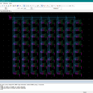
Full-Array Boolean Logic CIM Macro with Self-Recycling 10T-SRAM Cell for AES Systems
Base Paper Abstract:
Computing in memory (CIM), which alleviates the need to transfer a large amount of data between processor and memory, significantly reducing latency and energy consumption, is a promising new computing architecture for addressing the von Neumann bottleneck problem. This article proposes a CIM array structure composed of self-recycling 10T static random access memory (SRAM) cells, which can realize orthogonal data writing, and multiple Boolean logical operations for the entire array. The self-recycling and full-array activation characteristics are extremely suitable for accelerating diverse data processing algorithms such as the Advanced Encryption Standard (AES). A 4-kb SRAM is implemented in 55-nm CMOS technology to verify the effectiveness of the design. Compared with other state-of-threat architectures, the throughput and the operating frequency of the proposed CIM macro are increased to 843 GOPS/kb (2.64×) and 823.7 MHz (2.6×), respectively. The energy efficiency reaches 246.9 TOPS/W. When applied to the AES, the energy consumption is 35.77% less than the digital CIM architecture that is not self-recycling.
List of the following materials will be included with the Downloaded Backup:Provide Wordlwide Online Support
We can provide Online Support Wordlwide, with proper execution, explanation and additionally provide explanation video file for execution and explanations.
24/7 Support Center
NXFEE, will Provide on 24x7 Online Support, You can call or text at +91 9789443203, or email us nxfee.innovation@gmail.com
Terms & Conditions:
Customer are advice to watch the project video file output, and before the payment to test the requirement, correction will be applicable.
After payment, if any correction in the Project is accepted, but requirement changes is applicable with updated charges based upon the requirement.
After payment the student having doubts, correction, software error, hardware errors, coding doubts are accepted.
Online support will not be given more than 3 times.
On first time explanation we can provide completely with video file support, other 2 we can provide doubt clarifications only.
If any Issue on Software license / System Error we can support and rectify that within end of day.
Extra Charges For duplicate bill copy. Bill must be paid in full, No part payment will be accepted.
After payment, to must send the payment receipt to our email id.
Powered by NXFEE INNOVATION, Pondicherry.
Call us today at : +91 9789443203 or Email us at nxfee.innovation@gmail.com
NXFEE Development & Services

Copyright © 2026 Nxfee Innovation.