218 Products found
To develop and Implement Low Power, High Speed VLSI for Processing Signals using Multi rate Techniques Low Power Divider Using Vedic Mathematics
Abstract:
Multirate technique is necessary for systems with different input and output sampling rates. Recent advances in mobile computing and communication applications demand low power and high speed VLSI DSP systems. In this paper to discuss the downsampling technique and its improvement, major drawbacks of present approaches possible to increase degeneracy. This Multirate design methodology is systematic and applicable to many problems. The proposed architecture of this paper analysis the logic size, area and power consumption using Xilinx 14.2.The proposed architecture of this paper analysis the logic size, area and power consumption using Xilinx 14.2.
List of the following materials will be included with the Downloaded Backup:
MInSC: A VLSI Architecture for Myocardial Infarction Stages Classifier for Wearable Healthcare Applications
Base Paper Abstract:
Myocardial Infarction (MI) is a critical heart abnormality causing millions of fatalities worldwide every year. MI progress in three stages based on its severity causing several changes in an Electrocardiogram (ECG) signal. It is very critical to capture these variations, which requires continuous monitoring of the ECG signal of the patient. Therefore, it becomes imperative to develop a low power VLSI architecture to address the prognosis of MI. In this brief, for the first time, an area and power efficient design of a five stage classifier is proposed, which detects the progression of various stages of MI using ECG beats in real time. The proposed architecture has an area and total power utilization of 1.38mm2 and 5.12µW, respectively at SCL 180nm Bulk CMOS technology. The low power and area requirements and multiclass classification capability of the proposed design make it suitable to be used in wearable devices.
List of the following materials will be included with the Downloaded Backup:
Low power Dadda multiplier using approximate almost full adder and Majority logic based adder compressors
Base Paper Abstract:
An Approximate computing is widely used to have energy-efficient system design in Very Large-Scale Integration (VLSI). This approach is best suited for signal processing and multimedia applications where low power consumption is the main concern. Faster and significant results can be obtained from an approximate computing at the cost of reduced accuracy. In this work, we proposed a very novel design approaches based on various monolithic 4:2 compressors. Proposed approach is applied to have reduced stages in the partial product multiplication. Proposed Monolithic compressor had outperformed over various 4:2 compressors. Our proposed method is based on majority logic based with the use of Dadda multiplication. A new-partial product reduction format is implemented by this multiplier, which reduces the maximum output delay. This method of approach significantly reduces the utilization of number of MOSFETs compared to other multiplier such as Wallace Tree Multipliers. Simulation results are compared with conventional Dadda multiplier and ML based 4:2 compressors. Proposed approximate computing based almost full adder based majority logic based Dadda multiplier achieves reduction of 60.93% in area utilization 72.48% reduction in dynamic power reduction while processing time is also reduced by 72.98%. Dadda multiplication outperforms the other compressors.
List of the following materials will be included with the Downloaded Backup:
A VLSI-Based Hybrid ECG Compression Scheme for Wearable Sensor Node
Base Paper Abstract:
During smart long-term monitoring of any biomedical signal in wireless body area networks, wearable sensor nodes generate and transmit a large amount of data, increasing transmission power consumption. In order to reduce data storage and power consumption, a lossless data compression technique for an electrocardiogram signal monitoring system is presented in this letter. For this, a hybrid lossless compression algorithm based on Run-length coding and Golomb–Rice coding is proposed to enhance the bit compressing rate. The lossless encoding scheme is implemented on the MIT-BIH arrhythmia database, achieving a compression ratio of 2.91. A VLSI-based architecture of the data compression algorithm is implemented in 90nm CMOS technology that consumes power of 18.78 µW at 100 MHz operating frequency and 1.2 V supply voltage, occupying an area of 0.0051 mm2.
List of the following materials will be included with the Downloaded Backup:
Power Efficient Approximate Divider Architecture for Error Resilient Applications
Base Paper Abstract:
Approximate computing is an emerging paradigm in error-tolerant applications that leads to power-efficient designs without significant loss in quality. The divider in these applications have complex hardware and more latency among the computational blocks resulting in power consumption. Hence approximating the division module would lead to designs with vastly improved power efficiency. A new approximate subtractor (AxSUB) is proposed in this paper with the intent to reduce the hardware complexity while achieving accuracy within permissible limits. The proposed AxSUB and existing approximate subtractor units are used in the restoring array division (RAD) architecture to prove the efficacy of the AxSUB. Comprehensive error and synthesis analysis are performed on RAD architectures implemented using AxSUB, and existing methods. Our proposed design achieved a 21% decrease in area and a 28% decrease in power consumption compared to the exact design. The proposed and existing RAD architectures is implemented on change detection applications to validate the quality-effort tradeoff.
List of the following materials will be included with the Downloaded Backup:
Area and Power Efficient Truncated Booth Multipliers Using Approximate Carry-Based Error Compensation
Base Paper Abstract:
Approximate computing is a promising technique to elevate the performance of digital circuits at the cost of reduced accuracy in numerous error-resilient applications. Multipliers play a key role in many of these applications. In this brief, we propose a truncation based Booth multiplier with a compensation circuit generated by selective modifications in k-map to circumvent the carry appearing from the truncated part. By judicious mapping, hardware pruning and output error reduction is achieved simultaneously. In the quest of power and accuracy trade-off, Truncated and Approximate Carry based Booth Multipliers (TACBM) are proposed with a range of designs based on truncation factor w. When compared with the state-of-the-art multipliers, TACBM outperforms in terms of accuracy and Area Power savings. TACBM (w = 10) provides with 0.02% MRED and 23% reduction in Area-Power product compared to exact Booth multiplier. The multipliers are evaluated using image blending and Multilayer perceptron (MLP) neural network and a high value of accuracy (95.63%) for MLP is achieved.
List of the following materials will be included with the Downloaded Backup:
Power Efficient Tiny Yolo CNN Using Reduced Hardware Resources Based on Booth Multiplier and WALLACE Tree Adders
Base Paper Abstract:
Convolutional Neural Network (CNN) has attained high accuracy and it has been widely employed in image recognition tasks. In recent times, deep learning-based modern applications are evolving and it poses a challenge in research and development of hardware implementation. Therefore, hardware optimization for efficient accelerator design of CNN remains a challenging task. A key component of the accelerator design is a processing element (PE) that implements the convolution operation. To reduce the amount of hardware resources and power consumption, this article provides a new processing element design as an alternate solution for hardware implementation. Modified BOOTH encoding (MBE) multiplier and WALLACE tree-based adders are proposed to replace bulky MAC units and typical adder tree respectively. The proposed CNN accelerator design is tested on Zynq-706 FPGA board which achieves a throughput of 87.03 GOP/s for Tiny-YOLO-v2 architecture. The proposed design allows to reduce hardware costs by 24.5% achieving a power efficiency of 61.64 GOP/s/W that outperforms the previous designs.
List of the following materials will be included with the Downloaded Backup:
Energy-Efficient VLSI Realization of Binary64 Division With Redundant Number Systems
Base Paper Abstract:
VLSI realizations of digit-recurrence binary division usually use redundant representation of partial remainders and quotient digits. The former allows for fast carry-free computation of the next partial remainder, and the latter leads to less number of the required divisor multiples. In studying the previous relevant works, we have noted that the binary carry save (CS) number system is prevalent in the representation of partial remainders, and redundant high radix representation of quotient digits is popular in order to reduce the cycle count. In this paper, we explore a design space containing four division architectures. These are based on binary CS or radix-16 signed digit (SD) representations of partial remainders. On the other hand, they use full or partial pre computation of divisor multiples. The latter uses smaller multiplexer at the cost two extra adders, where one of the operands is constant within all cycles. The quotient digits are represented by radix-16 [−9,9]SDs. Our synthesis-based evaluation of VLSI realizations of the best previous relevant work and the four proposed designs show reduced power and energy figures in the proposed designs at the cost of more silicon area and delay measures. However, our energy-delay product is 26%–35% less than that of the reference work.
List of the following materials will be included with the Downloaded Backup:
Algorithm Level Error Detection in Low Voltage Systolic Array
Base Paper Abstract:
In this brief an approach is proposed to achieve energy savings from reduced voltage operation. The solution detects timing-errors by integrating Algorithm Based Fault Tolerance (ABFT) into a digital architecture. The approach has been studied with a systolic array matrix multiplier operating at reduced voltages, detecting errors on-the-fly to avoid energy demanding memory round-trips. The analysis of the solution has been done using analog-digital co-simulation to extract the transient behavior under different voltages and clock frequencies. HSPICE simulations using 90nm CMOS transistor models, and experiments by reducing operation voltage of an FPGA device were carried out. HSPICE simulations, showed possibility of 10x increase in energy-efficiency by approaching near-threshold region.
List of the following materials will be included with the Downloaded Backup:
Approximate Pruned and Truncated Haar Discrete Wavelet Transform VLSI Hardware for Energy-Efficient ECG Signal Processing
Abstract:
The approximate computing paradigm emerged as a key alternative for trading off accuracy and energy efficiency. Error-tolerant applications, such as multimedia and signal processing, can process the information with lower-than-standard accuracy at the circuit level while still fulfilling a good and acceptable service quality at the application level. The automatic detection of R-peaks in an electrocardiogram (ECG) signal is the essential step preceding ECG processing and analysis. The Haar discrete wavelet transform (HDWT) is a low-complexity pre-processing filter suitable to detect ECG R-peaks in embedded systems like wearable devices, which are incredibly energy constrained. This work presents an approximate HDWT hardware architecture for ECG processing at very high energy efficiency. Our best-proposal employing pruning within the approximate HDWT hardware architecture requires just seven additions. The use of a truncation technique to improve energy efficiency is also investigated herein by observing the evolution of the signal-to-noise ratio and the ultimate impact in the ECG peak-detection application. This research finds that our HDWT approximate hardware architecture proposal accepts higher truncation levels than the original HDWT. In summary: Our results show about 9 times energy reduction when combining our HDWT matrix approximation proposal with the pruning and the highest acceptable level of truncation while still maintaining the R-peak detection performance accuracy of 99.68% on average.
List of the following materials will be included with the Downloaded Backup:
A Reliable Low Standby Power 10T SRAM Cell With Expanded Static Noise Margins
Abstract:
This paper explores a low standby power 10T (LP10T) SRAM cell with high read stability and write-ability (RSNM/WSNM/WM). The proposed LP10T SRAM cell uses a strong cross-coupled structure consisting standard inverter with a stacked transistor and Schmitt-trigger inverter with a double-length pull-up transistor. This along with the read path separated from true internal storage nodes eliminates the read-disturbance. Furthermore, it performs its write operation in pseudo differential form through write bit line and control signal with a write-assist technique. To estimate the proposed LP10T SRAM cell’s performance, it is compared with some state-of-the-art SRAM cells using HSPICE in 16-nm CMOS predictive technology model at 0.7 V supply voltage under harsh manufacturing process, voltage, and temperature variations. The proposed SRAM cell offers 4.65X/1.57X/1.46X improvement in RSNM/WSNM/WM and 4.40X/1.69X narrower spread in RSNM/WM compared to the conventional 6T SRAM cell. Furthermore, it shows 1.26X/1.08X/1.01X higher RSNM/WSNM/WM and 1.71X/1.25X tighter/wider spread in RSNM/WM compared to the best studied SRAM cells. The proposed SRAM cell indicates 74.48%/1.41% higher/lower read/write delay compared to the 6T SRAM cell. Moreover, it exhibits the third-(second-) best read (write) dynamic power, consuming 29.69% (26.87%) lower than the 6T SRAM cell. The leakage power is minimized by the proposed design, which is 37.35% and 12.08% lower than that of the 6T and best studied cells, respectively. Nonetheless, the proposed LP10T SRAM cell occupies 1.313X higher area compared to the 6T SRAM cell.
List of the following materials will be included with the Downloaded Backup:
Soft-Error-Aware Read-Stability-Enhanced Low-Power 12T SRAM With Multi-Node Upset Recoverability for Aerospace Applications
Abstract:
With the advancement of technology, the size of transistors and the distance between them are reducing rapidly. Therefore, the critical charge of sensitive nodes is reducing, making SRAM cells, used for aerospace applications, more vulnerable to soft-error. If a radiation particle strikes a sensitive node of the standard 6T SRAM cell, the stored data in the cell are flipped, causing a single-event upset (SEU). Therefore, in this paper, a Soft-Error-Aware Read-Stability-Enhanced Low Power 12T (SARP12T) SRAM cell is proposed to mitigate SEUs. To analyze the relative performance of SARP12T, it is compared with other recently published soft-error-aware SRAM cells, QUCCE12T, QUATRO12T, RHD12T, RHPD12T and RSP14T. All the sensitive nodes of SARP12T can regain their data even if the node values are flipped due to a radiation strike. Furthermore, SARP12T can recover from the effect of single event multi-node upsets (SEMNUs) induced at its storage node pair. Along with these advantages, the proposed cell exhibits the highest read stability, as the ‘0’-storing storage node, which is directly accessed by the bit line during read operation, can recover from any upset. Furthermore, SARP12T consumes the least hold power. SARP12T also exhibits higher write ability and shorter write delay than most of the comparison cells. All these improvements in the proposed cell are obtained by exhibiting only a slightly longer read delay and consuming slightly higher read and write energy.
List of the following materials will be included with the Downloaded Backup:
Probability-Driven Evaluation of Lower-Part Approximation Adders
Abstract:
Parallel prefix adder topologies suffer from carry chains forming critical paths, limiting the performance and therefore the efficiency. We study approximation methods that offload the lower-part of calculation to an approximate unit and shorten the carry chain. We derive their accuracy models using probability theory. These models can replace Monte Carlo simulations. Furthermore, they can reveal better accuracy trade-offs without going through the RTL design, synthesis, and simulation of each unit and approximation level individually. Thus, they can eliminate the required design and simulation time and effort. After analyzing area-wise comparisons at varying number of approximated bits, we show that choosing a design that outperforms the others probabilistically also outperforms them in terms of accuracy, power, and performance trade-offs.
List of the following materials will be included with the Downloaded Backup:
A High-Throughput VLSI Architecture Design of Canonical Huffman Encoder
Abstract:
In this brief, a high-throughput Huffman encoder VLSI architecture based on the Canonical Huffman method is proposed to improve the encoding throughput and decrease the encoding time required by the Huffman code word table construction process. We proposed parallel computing architectures for frequency-statistical sorting and code-size computational sorting. This architecture results in a process of building a tree and assigning symbols that can be completed by scanning the data only once. This solves the problem of the low efficiency of the traditional algorithm, which needs to scan the data twice. Consequently, in addition to the advantages of the high compression ratio inherited from the Canonical Huffman, the proposed architecture has overridden advantages for a high parallelism processing capacity. The experimental results showed that the proposed architecture decreased the encoding time by 26.30% compared to the available Huffman encoder using the standard algorithm when encoding 256 8-bit symbols. Furthermore, the VLSI architecture could further decrease the encoding time when encoding more 8-bit symbols. In particular, when encoding 212,642 8-bit symbols, the proposed VLSI architecture could reduce the encoding time by 87.40%. Thus, compared with the traditional Huffman encoders, this brief achieved the improvement of coding efficiency.
List of the following materials will be included with the Downloaded Backup:
Low Cost Online Convolution Checksum Checker
Abstract:
Managing random hardware faults requires the faults to be detected online, thus simplifying recovery. Algorithm-based fault tolerance has been proposed as a low-cost mechanism to check online the result of computations against random hardware failures. In this case, the checksum of the actual result is checked against a predicted checksum computed in parallel by a hardware checker. In this work, we target the design of such checkers for convolution engines that are currently the most critical building block in image processing and computer vision applications. The proposed convolution checksum checker, named ConvGuard, utilizes a newly introduced invariance condition of convolution to predict implicitly the output checksum using only the pixels at the border of the input image. In this way, ConvGuard reduces the power required for accumulating the input pixels without requiring large buffers to hold intermediate checksum results. The design of ConvGuard is generic and can be configured for different output sizes and strides. The experimental results show that ConvGuard utilizes only a small percentage of the area/power of an efficient convolution engine while being significantly smaller and more power efficient than a state-of-the-art checksum checker for various practical cases.
List of the following materials will be included with the Downloaded Backup:
A Low Cost and High Throughtput FPGA Implementation of the Retinex Algorithm for Real Time Video Enhancement
Abstract:
For video applications in a special environment such as medical imaging, space exploration, and underwater exploration, the video captured by an image sensor is often deteriorated because of low lighting conditions. Therefore, it is necessary to enhance the part of the image that is too dark to distinguish details while maintaining the remaining part with the same brightness. The retinex algorithm is widely used to restore naturalness of a video, especially exhibiting outstanding performance in the enhancement of a dark area. However, it demands large computational complexity because of its intricate structure, such as the Gaussian filter and exponentiation operations, and consequently, it is difficult to process in real time. This article presents a low-cost and high-throughput design of the retinex video enhancement algorithm. The hardware (HW) design is implemented using a field-programmable gate array (FPGA), and it supports a throughput of 60 frames/s for a 1920 × 1080 image with negligible latency. The proposed FPGA design minimizes HW resources while maintaining the quality and the performance by using a small line buffer instead of a frame buffer, by applying the concept of approximate computing for the complex Gaussian filter, and by designing a new and nontrivial exponentiation operation. The proposed design makes it possible to significantly reduce HW resources (up to 79.22% of total resources) compared to existing systems and is compatible with commercialized devices through the standard HDMI/DVI video ports.
List of the following materials will be included with the Downloaded Backup:
A Three Stage Comparator and Its Modified Version With Fast Speed and Low Kickback
Abstract:
This brief presents a three-stage comparator and its modified version to improve the speed and reduce the kickback noise. Compared to the traditional two-stage comparators, the three-stage comparator in this work has an extra amplification stage, which enlarges the voltage gain and increases the speed. Unlike the traditional two-stage structure that uses pMOS input pair in the regeneration stage, the three-stage comparator makes it possible to use nMOS input pairs in both the regeneration stage and the amplification stage, further increasing the speed. Furthermore, in the proposed modified version of three-stage comparator, a CMOS input pair is adopted at the amplification stage. This greatly reduces the kickback noise by canceling out the nMOS kickback through the pMOS kickback. It also adds an extra signal path in the regeneration stage, which helps increase the speed further. For easy comparison, both the conventional two-stage and the proposed three-stage comparators are implemented in the same 130-nm CMOS process. Measured results show that the modified version of three-stage comparator improves the speed by 32%, and decreases the kickback noise by ten times. This improvement is not at the cost of increased input referred offset or noise.
List of the following materials will be included with the Downloaded Backup:
A 2.5-V 8-Bit Low power SAR ADC using POLC and SMTCMOS D-FF for IoT Applications
Abstract:
A 2.5-V 8-bit low force and efficient Successive Approximation Register Analog-to-Digital converter (SAR-ADC) utilizing a Principled Open Loop Comparator (POLC) and Switched Multi-Threshold Complementary Metal Oxide Semiconductor (SMTCMOS) D-FF shift Register. In light of high proficiency and low force applications SAR-ADC is increasingly well known, yet it experience the ill effects of resolution and speed confinements. To defeat the above issue proposed a systematic methodology uses low force POLC based SAR-ADC is structured. Considering about the resolution, speed and compact design of 8- bit SAR-ADC, the proposed POLC strategy reasonably diminishes the propagation delay by 37% and decreases the force utilization by 62% appeared differently in relation to the standard system. A D-flip flop is planned to employ SMTCMOS procedure which has low force utilization and productively decline the leakage power. All the above circuits are simulated by using TANNER-EDA tool in 0.25μm CMOS technology produces 97% Efficiency.
List of the following materials will be included with the Downloaded Backup:
Implementation of Low Power 1-bit Hybrid Full Adder using 22nm CMOS Technology
Abstract:
Adders are plays a vital role in digital and vlsi systems. Arithmetic operations are an essential part of digital systems. During VLSI systems, the entire research is on lowering the scale of transistors for enforcing any other digital system. This proposed architecture implemented by different types of logic systems; each logic performs the different role in the hybrid system. The hybrid Full Adder cell with one bit is implemented in this structure. The proposed method is investigated using 22-nm CMOS hybrid full adder. The proposed architecture demonstrates substantial efficiency in power consumption and delay, based on simulation results. The simulation result expressed that the full adder circuit is used to modern high speed central processing unit in the data path architecture. This form of hybrid Full Adder, reduces the delay and increasing efficiency and mainly used in nano technology applications. The average power consumption of 1.1055uW with moderately low delay of 7.0415 ps was found to be extremely low for 0.8-V supply at 22-nm technology. These kind of adder allocates significant improvements in power, high speed and area compared with previous full adder designs.
List of the following materials will be included with the Downloaded Backup:
A Low Power and High Speed Voltage Level Shifter Based on a Regulated Cross Coupled Pull Up Network
Abstract:
In this brief, a fast and very low power voltage level shifter (LS) is presented. By using a new regulated cross-coupled (RCC) pull-up network, the switching speed is boosted and the dynamic power consumption is highly reduced. The proposed (LS) has the ability to convert input signals with voltage levels much lower than the threshold voltage of a MOS device to higher nominal supply voltage levels. The presented LS occupies a small silicon area owing to its very low number of elements and is ultra-low-power, making it suitable for low-power applications such as implantable medical devices and wireless sensor networks. Results of the post-layout simulation in a standard 0.18-μm CMOS technology show that the proposed circuit can convert up input voltage levels as low as 80 mV. The power dissipation and propagation delay of the proposed level shifter for a low/high supply voltages of 0.4/1.8 V and input frequency of 1 MHz are 123.1 nW and 23.7 ns, respectively.
List of the following materials will be included with the Downloaded Backup:
Low-Cost and Programmable CRC Implementation Based on FPGA
Abstract:
Cyclic redundancy check (CRC) is a well-known error detection code that is widely used in Ethernet, PCIe, and other transmission protocols. The existing FPGA-based implementation solutions encounter the problem of excessive resource utilization in high-performance scenarios. The padding zeros problem and the introduction of programmability further exacerbate this problem. In this brief, the stride-by-5 algorithm is proposed to achieve the optimal utilization of FPGA resources. The pipelining go back algorithm is proposed to solve the padding zeros problem. The method of reprogramming by HWICAP is proposed to realize programmability with small and constant resource utilization. The experimental results show that the resource utilization of the proposed non-segmented architecture is 80.7%-87.5% and 25.1%-46.2% lower than that of two state of-the-art FPGA-based CRC implementations, and the proposed segmented architecture has lower resource utilization, by 81.7%- 85.9% and 2.9%-20.8%, than two state-of-the-art architectures. Furthermore, throughput and programmability are guaranteed.
List of the following materials will be included with the Downloaded Backup:
Design of ultra-low power consumption approximate 4-2 compressors based on the compensation characteristic
Abstract:
Approximate computing is tentatively applied in some digital signal processing applications which have an inherent tolerance for erroneous computing results. The approximate arithmetic blocks are utilized in them to improve the electrical performance of these circuits. Multiplier is one of the fundamental units in computer arithmetic blocks. Moreover, the 4-2 compressors are widely employed in the parallel multipliers to accelerate the compression process of partial products. In this paper, three novel approximate 4-2 compressors are proposed and utilized in 8-bit multipliers. Meanwhile, an error-correcting module (ECM) is presented to promote the error performance of approximate multiplier with the proposed 4-2 compressors. In this paper, the number of the approximate 4-2 compressor’s outputs is innovatively reduced to one, which brings further improvements in the energy efficiency. Compared with the exact 4-2 compressors, the simulation results indicate that the proposed approximate compressors UCAC1, UCAC2, UCAC3 achieve 24.76%, 51.43%, and 66.67% reduction in delay, 71.76%, 83.06%, and 93.28% reduction in power and 54.02%, 79.32%, and 93.10% reduction in area, respectively. And the utilization of these proposed compressors in 8-bit multipliers brings 49.29% reduction of power consumption on average.
List of the following materials will be included with the Downloaded Backup:
FPGA implementation of low power and high speed image edge detection algorithm
Abstract:
Image processing is a vital task in data processing system for applications in medical fields, remote sensing, microscopic imaging etc., Algorithms for processing image exist except for real time system style, hardware implementation is most popular principally. This paper presents a design for Sobel filter based edge detection on Field Programmable Gate Array (FPGA) board. Hardware implementation of the Sobel edge detection algorithm is chosen because it presents an honest scope for similarity over software package. On the opposite hand, Sobel edge detection will work with less deterioration in high level of noise. Edges are primarily the noticeable variation of intensities in a picture. Edges facilitate to spot the placement of an object and also the boundary of a selected entity within the image. It conjointly helps in feature extraction and pattern recognition. Hence, edge detection is of nice importance in pc vision. The planned design for edge detection exploitation Sobel algorithm is designed using structural Verilog lipoprotein synthesized exploitation Cadence Genus and enforced using Cadence Innovus. The practicality of the planning is verified exploitation normal pictures by FPGA implementation. The proposed architecture reduce the power, delay and space complexity compare to three existing architectures.
List of the following materials will be included with the Downloaded Backup:
High Speed Area Efficient VLSI Architecture of Three Operand Binary Adder
Abstract:
Three-operand binary adder is the basic functional unit to perform the modular arithmetic in various cryptography and pseudorandom bit generator (PRBG) algorithms. Carry save adder (CS3A) is the widely used technique to perform the three-operand addition. However, the ripple-carry stage in the CS3A leads to a high propagation delay of O(n). Moreover, a parallel prefix two-operand adder such as Han-Carlson (HCA) can also be used for three-operand addition that significantly reduces the critical path delay at the cost of additional hardware. Hence, a new high-speed and area-efficient adder architecture is proposed using pre-compute bitwise addition followed by carry prefix computation logic to perform the three-operand binary addition that consumes substantially less area, low power and drastically reduces the adder delay to O(log2 n). The proposed architecture is implemented on the FPGA device for functional validation and also synthesized with the commercially available 32nm CMOS technology library. The post-synthesis results of the proposed adder reported 3.12, 5.31 and 9.28 times faster than the CS3A for 32-, 64- and 128- bit architecture respectively. Moreover, it has a lesser area, lower power dissipation and smaller delay than the HC3A adder. Also, the proposed adder achieves the lowest ADP and PDP than the existing three-operand adder techniques.
List of the following materials will be included with the Downloaded Backup:
Comparison and Extension of Approximate 4-2 Compressors for Low-Power Approximate Multipliers
Abstract:
Approximate multipliers attract a large interest in the scientific literature that proposes several circuits built with approximate 4-2 compressors. Due to the large number of proposed solutions, the designer who wishes to use an approximate 4-2 compressor is faced with the problem of selecting the right topology. In this paper, we present a comprehensive survey and comparison of approximate 4-2 compressors previously proposed in literature. We present also a novel approximate compressor, so that a total of twelve different approximate 4-2 compressors are analyzed. The investigated circuits are employed to design 8 × 8 and 16 × 16 multipliers, implemented in 28nm CMOS technology. For each operand size we analyze two multiplier configurations, with different levels of approximations, both signed and unsigned. Our study highlights that there is no unique winning approximate compressor topology since the best solution depends on the required precision, on the signedness of the multiplier and on the considered error metric.
List of the following materials will be included with the Downloaded Backup:
Design of a Scalable Low Power 1 bit Hybrid Full Adder for Fast Computation
Abstract:
A novel design of a hybrid Full Adder (FA) using Pass Transistors (PTs), Transmission Gates (TGs) and Conventional Complementary Metal Oxide Semiconductor (CCMOS) logic is presented. Performance analysis of the circuit has been conducted using Cadence toolset. For comparative analysis, the performance parameters have been compared with twenty existing FA circuits. The proposed FA has also been extended up to a word length of 64 bits in order to test its scalability. Only the proposed FA and five of the existing designs have the ability to operate without utilizing buffer in intermediate stages while extended to 64 bits. According to simulation results, the proposed design demonstrates notable performance in power consumption and delay which accounted for low power delay product. Based on the simulation results, it can be stated that the proposed hybrid FA circuit is an attractive alternative in the data path design of modern high-speed Central Processing Units.
List of the following materials will be included with the Downloaded Backup:
Design and analysis of High speed Wallace tree multiplier using parallel prefix adders for VLSI circuit designs
Abstract:
Major operation block in any processing unit is a multiplier. There are many multiplication algorithms are proposed, by using which multiplier structure can be designed. Among various multiplication algorithms, Wallace tree multiplication algorithm is beneficial in terms of speed of operation. With the advancement of technology, demand for circuits with high speed and low area is increasing. In order to improve the speed of Wallace tree multiplier without degrading its area parameter, a new structure of Wallace tree multiplier is proposed in this paper. In the proposed structure, the final addition stage of partial products is performed by parallel prefix adders (PPAs). In this paper, five Wallace tree multiplier structures are proposed using Kogge stone adder, Sklansky adder, Brent Kung adder, Ladner Fischer adder and Han carlson adder. All the multiplier structures are designed using Verilog HDL in Xilinix 13.2 design suite. The proposed structures are simulated using ISIM simulator and synthesized using XST synthesizer. The proposed designs are analyzed with respect to traditional multiplier design in terms of area (No. of LUTs) and delay (ns).
List of the following materials will be included with the Downloaded Backup: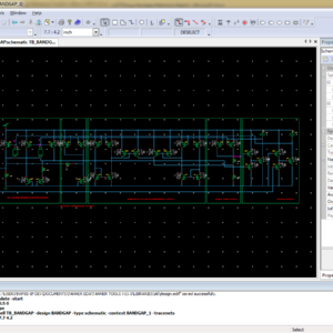
Low-Voltage Bandgap Reference Circuit in 28nm CMOS
Abstract:
This paper presents a hybrid adjusted temperature compensation circuit for reducing the temperature drift of the bandgap reference. Combining first-order bandgap current, nonlinear compensation current, and temperature curvature compensation current together, a temperature insensitive reference voltage can be obtained in proposed circuit. Designed and verified in UMC 28nm CMOS technology with Cadence IC615, the proposed circuit achieves a post-layout simulation temperature drift of 5.48 ppm/°C in the range of -20°C to 120°C with a supply voltage of 1.05-V.
List of the following materials will be included with the Downloaded Backup:
Highly Linear Low-Power Wireless RF Receiver for WSN
Abstract:
This paper introduces a low-power wireless RF receiver for the wireless sensor network. The receiver has improved linearity with incorporated current-mode circuits and high-selectivity filtering. The receiver operates at the 900-MHz industrial, scientific, and medical band and is implemented in 130-nm CMOS technology. The receiver has a frequency multiplication mixer, which uses a 300-MHz clock from a local oscillator (LO). The LO is implemented using vertical delay cells to reduce power consumption. The receiver conversion gain is 40 dB and the receiver noise. The receiver’s input third-order intercept point (IIP3) is −6 dBm and the total power consumption is 1.16 mW.
List of the following materials will be included with the Downloaded Backup:
Column-Selection-Enabled 10T SRAM Utilizing Shared Diff-VDD Write and Dropped-VDD Read for Power Reduction
Abstract:
A non-destructive column-selection-enabled 10T SRAM for aggressive power reduction is presented in this brief. It frees a half-selected behavior by exploiting the bit line-shared data-aware write scheme. The differential-VDD (Diff-VDD) technique is adopted to improve the write ability of the design. In addition, its decoupled read bit lines are given permission to be charged and discharged depending on the stored data bits. In combination with the proposed dropped-VDD biasing, it achieves the significant power reduction. The experimental results show that the proposed design provides the 3.3× improvement in the write margin compared with the standard Diff-10T SRAM. A 5.5-kb 10T SRAM in a 65-nm CMOS process has a total power of 51.25 µW and a leakage power of 41.8 µW when operating at 6.25 MHz at 0.5 V, achieving 56.3% reduction in dynamic power and 32.1% reduction in leakage power compared with the previous single-ended 10T SRAM.
List of the following materials will be included with the Downloaded Backup:
Instantaneous Power Consuming Level Shifter for Improving Power Conversion Efficiency of Buck Converter
Abstract:
An instantaneous power consuming level shifter is presented in this paper to increase the DC converter efficiency. The level shifter is used in a high-side power switch driver to remove the external capacitor which is used in bootstrap technique. The level shifter consumes power only during the transition period. A delay cell is used to turn the level shifter off to reduce the power consumption period. An output voltage detector is added to turn the level shifter off even before the delay time. An asynchronous discontinuous conduction mode buck converter is designed to verify the performance of the level shifter. Simulation results show that the power consumption of the proposed level shifter decreased by 66%, while the converter efficiency increased by the maximum of 9% compared to results obtained for a conventional level shifter. The converter is fabricated using the TSMC 0.18-µm BCD process and it operates within an input range of 2–5 V when the current varies from 400 µA to 18 mA and delivers an output voltage of 1.8 V.
List of the following materials will be included with the Downloaded Backup:
Many-Objective Sizing Optimization of a Class-C/D VCO for Ultralow-Power IoT and Ultralow Phase-Noise Cellular Applications
Abstract:
In this paper, the performance boundaries and corresponding tradeoffs of a complex dual-mode class-C/D voltage controlled oscillator (VCO) are extended using a framework for the automatic sizing of radio frequency integrated circuit blocks, where an all-inclusive test bench formulation enhanced with an additional measurement processing system enables the optimization of “everything at once” toward its true optimal tradeoffs. VCOs embedded in the state-of-the-art multi standard transceivers must comply with extremely high performance and ultralow power requirements for modern cellular and Internet of Things applications. However, the proper analysis of the design tradeoffs is tedious and impractical, as a large amount of conflicting performance figures obtained from multiple modes, test benches, and/or analysis must be considered simultaneously. Here, the dual-mode design and optimization conducted provided 287 design solutions with figures of merit above 192 dBc/Hz, where the power consumption varies from 0.134 to 1.333 mW, the phase noise at 10 MHz from −133.89 to −142.51 dBc/Hz, and the frequency pushing from 2 to 500 MHz/V, on the worst case of the tuning range. These results pushed this circuit design to its performance limits on a 65-nm CMOS technology, reducing 49% of the power consumption of the original design while also showing its potential for ultralow power with more than 93% reduction. In addition, worst case corner criteria were also performed on the top of the worst case tuning range optimization, taking the problem to a human-untrea table LXVI-D performance space.
List of the following materials will be included with the Downloaded Backup:
Analysis, Comparison, and Experimental Validation of a Class AB Voltage Follower With Enhanced Bandwidth and Slew Rate
Abstract:
This paper describes a bandwidth (BW)- and slew rate (SR)-enhanced class AB voltage follower (VF). A thorough small signal analysis of the proposed and a state-of-the-art AB-enhanced VF is presented to compare their performance. The proposed circuit has 50-MHz BW, 19.5-V/µs SR, and a BW figure of merit of 41.6 (MHz × pF/µW) for CL = 50 pF. It provides 13 times higher current efficiency and 15 times higher BW than the conventional VF with equal 60-µW static power dissipation. The experimental and simulation results of a fabricated test chip in the 130-nm CMOS technology validate the proposed circuit.
List of the following materials will be included with the Downloaded Backup:
A Nanopower Biopotential Lowpass Filter Using Subthreshold Current-Reuse Biquads With Bulk Effect Self-Neutralization
Abstract:
A nanopower CMOS 4th-order lowpass filter suitable for biomedical applications is presented. The filter is formed by cascading two types of subthreshold current-reuse biquadratic cell. Each proposed cell is capable of neutralizing the bulk effect that induces the passband attenuation. The nearly 0-dB passband gain can thus be maintained, while the entire filter circuit remains compact and power-efficient. Designed for electrocardiogram detection as an example of application, the filter prototype has been fabricated in a 0.35 µm CMOS process occupying 269 µm × 383 µm chip area. Measurements verify that the filter can operate from a 1.5-V single supply and consumes 5.25 nW, while providing a cutoff frequency of 100 Hz and input-referred noise of 39.38 µVrms. The intermodulation-free dynamic range of 51.48 dB is obtained from a two-tone test of 50 and 60 Hz input frequencies. Compared with state-of-the-art nanopower lowpass filters using the most relevant and reasonable figure of merit, the proposed filter ranks the best.
List of the following materials will be included with the Downloaded Backup: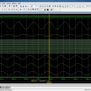
Low-Complexity 2-D Digital FIR Filters Using Polyphase Decomposition and Farrow Structure
Abstract:
This paper proposes a novel realization technique for quadrantally symmetric 2-D finite impulse response filters with a guaranteed reduction in the hardware complexity. Here, the concept of Farrow structure-based interpolation filter design using the polyphase decomposition of the 1-D filter transfer function is effectively utilized in the 2-D domain. The proposed 2-D filter makes use of row-wise polyphase decomposition of the 2-D transfer function or frequency response, followed by the polynomial approximation of the individual polyphase coefficients resulting in Farrow structures corresponding to each row filter. The final coefficients are implemented by varying the delay values in all the Farrow structures, followed by the interpolation of the coefficients obtained from each delay value, which in turn forms the rows in the 2-D kernel. The major highlight of the proposed method is the highly reduced implementation complexity in terms of the number of multipliers and adders, with a low normalized root-mean-square error. Design examples of the circularly symmetric and fan-type filters have been considered to show the efficiency of the approach. The results show a drastic reduction in the implementation complexity of the 2-D filters of upto 20%, with significantly low normalized root-mean-square error lesser than 0.5%.
List of the following materials will be included with the Downloaded Backup: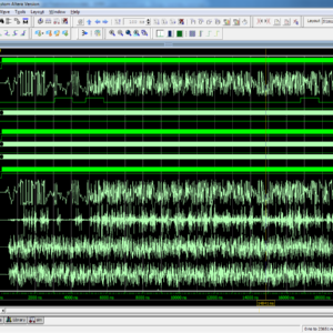
VLSI Design of SVM-Based Seizure Detection System With On-Chip Learning Capability
Abstract:
Portable automatic seizure detection system is very convenient for epilepsy patients to carry. In order to make the system on-chip trainable with high efficiency and attain high detection accuracy, this paper presents a very large scale integration (VLSI) design based on the nonlinear support vector machine (SVM). The proposed design mainly consists of a feature extraction (FE) module and an SVM module. The FE module performs the three level Daubechies discrete wavelet transform to fit the physiological bands of the electroencephalogram (EEG) signal and extracts the time–frequency domain features reflecting the non stationary signal properties. The SVM module integrates the modified sequential minimal optimization algorithm with the table-driven-based Gaussian kernel to enable efficient on-chip learning. The presented design is verified on an Altera Cyclone II field-programmable gate array and tested using the two publicly available EEG datasets. Experiment results show that the designed VLSI system improves the detection accuracy and training efficiency.
List of the following materials will be included with the Downloaded Backup: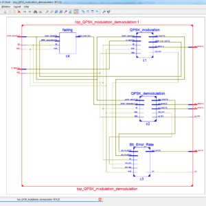
A Low Complexity I/Q Imbalance Calibration Method for Quadrature Modulator
Abstract:
This brief presents a low-complexity I/Q (in-phase and quadrature components) imbalance calibration method for the transmitter using quadrature modulation. Impairments in analog quadrature modulator have a deleterious effect on the signal fidelity. Among the critical impairments, I/Q imbalance (gain and phase mismatches) deteriorates the residual sideband performance of the analog quadrature modulator degrading the error vector magnitude. Based on the theoretical mismatch analysis of the quadrature modulator, we propose a low-complexity I/Q imbalance extraction algorithm. After the parameter extraction, the transmitter is calibrated by imposing the counter imbalanced mismatch of the transmitter through the digital baseband. In comparison with existing I/Q imbalance calibration methods, the novelty of the proposed method lies in that: 1) only three spectrum measurements of the device-under-test are needed for extraction and calibration of gain and phase mismatches; 2) due to the blind nature of the calibration algorithm, the proposed approach can be readily applicable to an existing I/Q transmitter; 3) no extra hardware that degrades the calibration accuracy is required; and 4) due to the non-iterative nature, the proposed method is faster and computationally more efficient than previously published methods.
List of the following materials will be included with the Downloaded Backup: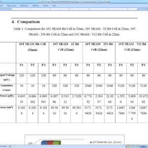
Low-Power Near-Threshold 10T SRAM Bit Cells With Enhanced Data-Independent Read Port Leakage for Array Augmentation in 32-nm CMOS
Abstract:
The conventional six-transistor static random access memory (SRAM) cell allows high density and fast differential sensing but suffers from half-select and read-disturb issues. Although the conventional eight-transistor SRAM cell solves the read-disturb issue, it still suffers from low array efficiency due to deterioration of read bit-line (RBL) swing and Ion/Ioff ratio with increase in the number of cells per column. Previous approaches to solve these issues have been afflicted by low performance, data dependent leakage, large area, and high energy per access. Therefore, in this paper, we present three iterations of SRAM bit cells with nMOS-only based read ports aimed to greatly reduce data dependent read port leakage to enable 1k cells/RBL, improve read performance, and reduce area and power over conventional and 10T cell-based works. We compare the proposed work with other works by recording metrics from the simulation of a 128-kb SRAM constructed with divided-word line-decoding architecture and a 32-bit word size. Apart from large improvements observed over conventional cells, up to 100-mV improvement in read-access performance, up to 19.8% saving in energy per access, and up to 19.5% saving in the area are also observed over other 10T cells, thereby enlarging the design and application gamut for memory designers in low-power sensors and battery-enabled devices.
List of the following materials will be included with the Downloaded Backup:
Low-Power Approximate Unsigned Multipliers with Configurable Error Recovery
Abstract:
Approximate circuits have been considered for applications that can tolerate some loss of accuracy with improved performance and/or energy efficiency. Multipliers are key arithmetic circuits in many of these applications including digital signal processing (DSP). In this paper, a novel approximate multiplier with a low power consumption and a short critical path is proposed for high-performance DSP applications. This multiplier leverages a newly designed approximate adder that limits its carry propagation to the nearest neighbors for fast partial product accumulation. Different levels of accuracy can be achieved by using either OR gates or the proposed approximate adder in a configurable error recovery. The multipliers using these two error reduction strategies are referred to as approximate multiplier 1 (AM1) and approximate multiplier 2 (AM2), respectively. Both AM1 and AM2 have a low mean error distance, i.e., most of the errors are not significant in magnitude. Compared to a Wallace multiplier optimized for speed, an 8×8 AM1 with 4 MSBs (most significant bits) for error reduction and synthesized using a 28 nm CMOS process shows a 60% reduction in delay (when optimized for delay) and a 42% reduction in power dissipation (when optimized for area). In a 16×16 design, half of the least significant partial products are truncated for AM1 and AM2, which are thus denoted as TAM1 and TAM2, respectively. Compared with the Wallace multiplier, TAM1 and TAM2 save from 50% to 66% in power, when optimized for area. Compared to existing approximate multipliers, AM1, AM2, TAM1 and TAM2 show significant advantages in accuracy with a high performance. AM2 has a better accuracy compared to AM1 but with a longer delay and higher power consumption. Image processing applications including image sharpening and smoothing are considered to show the quality of the approximate multipliers in error-tolerant applications. By utilizing an appropriate error recovery, the proposed approximate multipliers achieve similar processing accuracy as traditional exact multipliers, but with significant improvements in power.
List of the following materials will be included with the Downloaded Backup:
Radiation-Hardened 14T SRAM Bit cell With Speed and Power Optimized for Space Application
Abstract:
In this paper, a novel radiation-hardened 14-transistor SRAM bit cell with speed and power optimized [radiation-hardened with speed and power optimized (RSP)-14T] for space application is proposed. By circuit- and layout-level optimization design in a 65-nm CMOS technology, the 3-D TCAD mixed-mode simulation results show that the novel structure is provided with increased resilience to single-event upset as well as single-event–multiple-node upsets due to the charge sharing among OFF-transistors. Moreover, the HSPICE simulation results show that the write speed and power consumption of the proposed RSP-14T are improved by ∼65% and ∼50%, respectively, compared with those of the radiation hardened design (RHD)-12T memory cell.
List of the following materials will be included with the Downloaded Backup: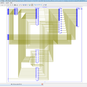
A Decoder for Short BCH Codes With High Decoding Efficiency and Low Power for Emerging Memories
Abstract:
In this paper, a double-error-correcting and triple error-detecting (DEC-TED) Bose–Chaudhuri–Hocquenghem (BCH) code decoder with high decoding efficiency and low power for error correction in emerging memories is presented. To increase the decoding efficiency, we propose an adaptive error correction technique for the DEC-TED BCH code that detects the number of errors in a codeword immediately after syndrome generation and applies a different error correction algorithm depending on the error conditions. With the adaptive error correction technique, the average decoding latency and power consumption are significantly reduced owing to the increased decoding efficiency. To further reduce the power consumption, an invalid-transition-inhibition technique is proposed to remove the invalid transitions caused by glitches of syndrome vectors in the error-finding block. Synthesis results with an industry-compatible 65-nm technology library show that the proposed decoders for the (79, 64, 6) BCH code take only 37%–48% average decoding latency and achieve more than 70% power reduction compared to the conventional fully parallel decoder under the 10−4–10−2 raw bit-error rate.
List of the following materials will be included with the Downloaded Backup: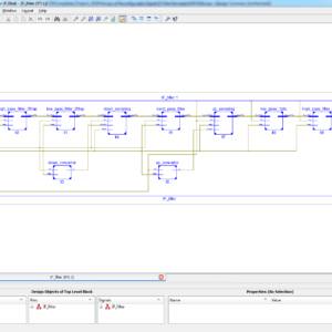
Design of Reconfigurable Digital IF Filter with Low Complexity
Abstract:
Due to limited frequency resources, new services are being applied to the existing frequencies, and service providers are allocating some of the existing frequencies for newly enhanced mobile communications. Because of this frequency environment, repeater and base station systems for mobile communications are becoming more complicated, and frequency interference caused by multiple bands and services is getting worse. Therefore, a heterodyne receiver using IF filters with high selectivity has been used to minimize the interference between frequencies. However, repeater and base station systems in mobile communications employing fixed IF filters cannot actively cope with the usage of multiple frequency bands, the application of various services, and frequency recycling. Therefore, this brief proposes a reconfigurable digital IF filter with variable center frequency and bandwidth while achieving high selectivity as existing IF filters. The center frequency of filter can vary from 10MHz to 62.5MHz, and the filter bandwidth can be selective to one of 10MHz, 15MHz, and 20MHz. The proposed digital filter also reduces the complexity of adders and multipliers by 38.81% and 41.57%, respectively, compared to an existing digital filter by using a filter bank and a multi stage structure. This digital IF filter is fabricated on a 130-nm CMOS process and occupies 5.90 mm2.
List of the following materials will be included with the Downloaded Backup:
Low Power and High Speed Implementation of FIR filter design using CMOS GDI Truncated Multiplier
Abstract:
The logic size, propagation delay, power of applications, based upon this improvement the adder design logic size will reduced year by year, here a proposed In recent technology of any application, adders is a more priority to do a function and task of arithmetic operation, in crucial this adder based arithmetic operation will decide work of this paper will design using a single bit full adder to design a multiplier. In this multiplier design, adder is a main priority to reduce the arithmetic logic size and increases speed of multiplier, in recent we have lots of multiplier design, Vedic multiplier, Wallace tree multiplier, booth multiplier, approximate multiplier. Here, the proposed work will taken truncated multiplier design, it's because, the truncated multiplier will have a capability to reduced internal and external architecture size in every design, regarding this truncated multiplier will have three options such as rounding, deleting, truncating, here the MSB bits will be truncated and present the output of n x n multiplication will provided only n bit level, using this truncated multiplier the proposed work will designed a 8-Tap FIR(Finite impulse response) filter and shown the efficiency of filter design using this CMOS GDI (Gate Diffusion Input) adder design. This proposed work will design in CMOS Logic gate and which 10-T transistor level of full adders with 90um technology, finally proved the terms of area, delay and power.
List of the following materials will be included with the Downloaded Backup:
High speed and low power preset-able modified TSPC D flip-flop design and performance comparison with TSPC D flip-flop
Abstract:
Positron emission tomography (PET) is a nuclear functional imaging technique that produces a three-dimensional image of functional organs in the body. PET requires high resolution, fast and low power multichannel analog to digital converter (ADC). A typical multichannel ADC for PET scanner architecture consists of several blocks. Most of the blocks can be designed by using fast, low power D flip-flops. A preset-able true single phase clocked (TSPC) D flip-flop shows numerous glitches (noise) at the output due to unnecessary toggling at the intermediate nodes. Preset-able modified TSPC (MTSPC) D flip flop have been proposed as an alternative solution to alleviate this problem. However, the MTSPC D flip-flop requires one extra PMOS to suspend toggling of the intermediate nodes. In this work, we designed a 7-bit preset-able gray code counter by using the proposed D flip-flop. This work involves UMC 180 nm CMOS technology for preset-able 7-bit gray code counter where we achieved 1 GHz maximum operation frequency with most significant bit (MSB) delay 0.96 ns, power consumption 244.2 μW (micro watt) and power delay product (PDP) 0.23 pJ (Pico joule) from 1.8 V power supply.
List of the following materials will be included with the Downloaded Backup:
An Efficient VLSI Architecture for Convolution Based DWT Using MAC
Abstract:
The modern real time applications related to image processing and etc., demand high performance discrete wavelet transform (DWT). This paper proposes the floating point multiply accumulate circuit (MAC) based 1D/2D-DWT, where the MAC is used to find the outputs of high/low pass FIR filters. The proposed technique is implemented with 45 nm CMOS technology and the results are compared with various existing techniques. The proposed 8 × 8-point floating point 2-levels 2D-DWT achieves 27.6% and 83.7% of reduction in total area and net power respectively as compared with existing DWT.
List of the following materials will be included with the Downloaded Backup:
Design of Low Power High Performance 2-4 and 4-16 Mixed-Logic Line Decoders
Abstract:
This paper introduces a mixed-logic design method for line decoders, combining transmission gate logic, pass transistor dual-value logic and static CMOS. Two novel topologies are presented for the 2-4 decoders: a 14-transistor topology aiming on minimizing transistor count and power dissipation and a 15-transistor topology aiming on high power delay performance. Both a normal and an inverting decoder are implemented in each case, yielding a total of four new designs. Furthermore, four new 4-16 decoders are designed, by using mixed-logic 2-4 pre decoders combined with standard CMOS post-decoder. All proposed decoders have full swinging capability and reduced transistor count compared to their conventional CMOS counterparts. Finally, a variety of comparative spice simulations at the 32 nm shows that the proposed circuits present a significant improvement in power and delay, outperforming CMOS in almost all cases.
List of the following materials will be included with the Downloaded Backup:
Low-Power and Fast Full Adder by Exploring New XOR and XNOR Gates
Abstract:
In this paper, novel circuits for XOR/XNOR and simultaneous XOR–XNOR functions are proposed. The proposed circuits are highly optimized in terms of the power consumption and delay, which are due to low output capacitance and low short-circuit power dissipation. We also propose six new hybrid 1-bit full-adder (FA) circuits based on the novel full-swing XOR–XNOR or XOR/XNOR gates. Each of the proposed circuits has its own merits in terms of speed, power consumption, power delay product (PDP), driving ability, and so on. To investigate the performance of the proposed designs, extensive HSPICE and Cadence Virtuoso simulations are performed. The simulation results, based on the 65-nm CMOS process technology model, indicate that the proposed designs have superior speed and power against other FA designs. A new transistor sizing method is presented to optimize the PDP of the circuits. In the proposed method, the numerical computation particle swarm optimization algorithm is used to achieve the desired value for optimum PDP with fewer iterations. The proposed circuits are investigated in terms of variations of the supply and threshold voltages, output capacitance, input noise immunity, and the size of transistors.
List of the following materials will be included with the Downloaded Backup:
A Low-Voltage Radiation-Hardened 13T SRAM Bit cell for Ultralow Power Space Applications
Proposed Abstract:
Continuous transistor scaling, coupled with the growing demand for low-voltage, low-power applications, increases the susceptibility of VLSI circuits to soft-errors, especially when exposed to extreme environmental conditions, such as those encountered by space applications. The most vulnerable of these circuits are memory arrays that cover large areas of the silicon die and often store critical data. Radiation hardening of embedded memory blocks is commonly achieved by implementing extremely large bitcells or redundant arrays and maintaining a relatively high operating voltage; however, in addition to the resulting area overhead, this often limits the minimum operating voltage of the entire system leading to significant power consumption. In this paper, we propose the first radiation-hardened static random access memory (SRAM) bitcell targeted at low-voltage functionality, while maintaining high soft-error robustness. A 32×32 bit memory macro was designed and fabricated in a standard 0.13-µm CMOS process, showing full read and write functionality down to the subthreshold voltage of 300 mV. This is achieved with a cell layout that is only 2×larger than a reference 6T SRAM cell drawn with standard design rules. The proposed architecture of this paper is analysis the logic size, area and power consumption using tanner tool.
List of the following materials will be included with the Downloaded Backup:
Low-Complexity VLSI Design of Large Integer Multipliers for Fully Homomorphic Encryption
Abstract:
Large integer multiplication has been widely used in fully homomorphic encryption (FHE). Implementing feasible large integer multiplication hardware is thus critical for accelerating the FHE evaluation process. In this paper, a novel and efficient operand reduction scheme is proposed to reduce the area requirement of radix-r butterfly units. We also extend the single port, merged-bank memory structure to the design of number theoretic transform (NTT) and inverse NTT (INTT) for further area minimization. In addition, an efficient memory addressing scheme is developed to support both NTT/INTT and resolving carries computations. Experimental results reveal that significant area reductions can be achieved for the targeted 786 432- and 1 179 648-bit NTT-based multipliers designed using the proposed schemes in comparison with the related works. Moreover, the two multiplications can be accomplished in 0.196 and 2.21 ms, respectively, based on 90-nm CMOS technology. The low-complexity feature of the proposed large integer multiplier designs is thus obtained without sacrificing the time performance.
List of the following materials will be included with the Downloaded Backup: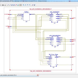
High Performance VLSI architecture for M-PSK modems
Abstract:
M-PSK (phase shift keying) modulation schemes are used in many high-speed applications like satellite communication, as they are more bandwidth and power efficient compared with other schemes. This study presents very large scale integrated circuits (VLSI) architectures for modulators and demodulators of quadrature phase shift keying (QPSK), 4PSK, 8PSK and 16PSK systems, based on the principle of direct digital synthesis. The proposed modulators do not use any multiplier in contrast to the conventional modulators and hence they are relatively fast and area efficient. Based on the coherent detection technique, this study proposes new demodulation algorithms for 4PSK, 8PSK and 16PSK systems which can be implemented both in analogue and digital domains. This study also presents VLSI architectures for all the proposed algorithms. The proposed architectures are described in VHDL and implemented on Xilinx field programmable gate arrays (FPGAs). The simulation results verify their functional validity and implementation results show the suitability of the proposed architectures for satellite communications.
List of the following materials will be included with the Downloaded Backup:Provide Wordlwide Online Support
We can provide Online Support Wordlwide, with proper execution, explanation and additionally provide explanation video file for execution and explanations.
24/7 Support Center
NXFEE, will Provide on 24x7 Online Support, You can call or text at +91 9789443203, or email us nxfee.innovation@gmail.com
Terms & Conditions:
Customer are advice to watch the project video file output, and before the payment to test the requirement, correction will be applicable.
After payment, if any correction in the Project is accepted, but requirement changes is applicable with updated charges based upon the requirement.
After payment the student having doubts, correction, software error, hardware errors, coding doubts are accepted.
Online support will not be given more than 3 times.
On first time explanation we can provide completely with video file support, other 2 we can provide doubt clarifications only.
If any Issue on Software license / System Error we can support and rectify that within end of day.
Extra Charges For duplicate bill copy. Bill must be paid in full, No part payment will be accepted.
After payment, to must send the payment receipt to our email id.
Powered by NXFEE INNOVATION, Pondicherry.
Call us today at : +91 9789443203 or Email us at nxfee.innovation@gmail.com
NXFEE Development & Services

Product Categories
- 2014 (12)
- 2015 (39)
- 2016 (31)
- 2017 (16)
- 2018 (17)
- 2019 (42)
- 2020 (29)
- 2021 (16)
- 2022 (22)
- 2023 (17)
- Area Efficient (92)
- High speed VLSI Design (49)
- IEEE (16)
- Image Processing (34)
- Low power VLSI Design (71)
- NOC VLSI Design (3)
- VLSI (180)
- VLSI Application / Interface and Mini Projects (13)
- VLSI_2023 (15)
Filter by price
Product Status
Sort by producents

Copyright © 2021 Nxfee Innovation.